User's Guide
SLCU001 – May 2016
TRS3122EEVM User's Guide
Abstract
This user's guide describes the functional operation of the TRS3122EEVM Evaluation Module (EVM) for
use as a design reference as well as a general engineering demonstration for the TRS3122E RS-232
Transceiver. Included in this User's Guide are setup instructions, features, a schematic diagram, an
example layout, layout guidelines, and a bill of materials.
Introduction
The TRS3122EEVM is an evaluation module for the TRS3122E device, a 1.8-V high-speed RS-232
transceiver. The module enables device evaluation using the installed DB9 connector and terminal block.
The board interfaces data and control CMOS logic levels on the terminal block to RS-232 levels
supporting data [RX, TX] channels and flow control [RTS, CTS] channels on the DB9 connector.
TRS3122EEVM Board
Features
•
•
•
•
•
•
Interface with MCUs or processor from 1.65 V up to 5.5 V
High-speed RS-232 communication, up to 1 Mbps
Auto-powerdown plus for very low power consumption (1µA) during shutdown
Robust IEC61000-4-2 qualification provides robust protection from electrostatic discharge events
DB9 female connector for direct connection with a computer's RS-232 port
Screw terminals for easy connection for all power and logic signals
SLCU001 – May 2016
Submit Documentation Feedback
TRS3122EEVM User's Guide
Copyright © 2016, Texas Instruments Incorporated
1
�www.ti.com
Applications
Any application that needs short range point to point full duplex data communications with hardware flow
control.
•
•
•
•
Remote Radio Unit (RRU)
Base Band Unit (BBU)
Electronic Point of Sale (EPOS)
Diagnostics & Data Transmission Battery-Powered Equipment
Setup
The VCC screw terminal point needs to be supplied with external power; 1.8 V or 3.3 V is recommended.
The VL screw terminal point needs to be supplied with external power; 1.8 V to VCC is recommended.
The GND screw terminal point is the ground connection for the TRS3122EEVM.
The DB9 connector mates with a personal computer's RS-232 port or a USB to RS-232 adapter. For initial
testing, external wires can be added to screw terminals; CTS2 to RTS2 and TX2 to RX2 to loop back the
signal.
The ideal usage involves connecting the terminal block data and control lines to a system that has an
UART (Universal asynchronous receiver/transmitter) onboard.
The EVM has pull up resistors on the TRS3122E FORCEOFF and FORCEON pins to keep both driver
and receiver active. If desired, these signal can be driven by the external system to fully control all the
features of auto-powerdown plus circuitry. The system may also benefit from monitoring the INVALID
output to detect if an active connection has been made to the RS-232 port.
Usage at 5 V
The capacitors installed on the TRS3122EEVM were selected for VCC = 1.8 V and VCC = 3.3 V
operation. It is required to change some of the onboard capacitors for 5 V testing.
Capacitor Changes
2
VCC voltage
C1
C2
C4
C5
1.8 V, 3.3 V
100 nF
100 nF
100 nF
100 nF
5V
47 nF
330 nF
330 nF
330 nF
TRS3122EEVM User's Guide
SLCU001 – May 2016
Submit Documentation Feedback
Copyright © 2016, Texas Instruments Incorporated
�www.ti.com
Connector/Test Points
DB9 Connector
DB9 Connector Pinout
The female DB9 port provides access to the TRS3122E device through a standard RS-232 pinout. The
TRS3122E female port is DCE to mate with a computer's male DTE port. The pin names are
counterintuitive on the DCE side. For example the RX pin on EVM is connected to a driver and TX
connects to a receiver.
• Pins 1 and 9 are not connected.
• Pins 2, 3, 7, 8 provide access to the RS-232 communication lines RX1, TX1, RTS1, CTS1 respectively.
• Pins 4 and 6 are shorted together by a 0 Ω resistor to loopback the unused handshaking lines.
• Pin 5 is grounded.
Screw Terminal Connector
Screw Terminal Connector Pinout
The screw terminal port provides access to the TRS3122E device communication pins as well as control,
output, and power pins. Note that pins are numbered from left to right in the description below.
• Pins 1 through 4 provide access to the logic communication lines CTS2, RX2, RTS2, and TX2
respectively.
• Pin 5 connects to the INVALID pin, which has the function described by the INVALID Pin Function
Table.
INVALID Pin Function
INPUTS
OUTPUT
RIN1, RIN2
FORCEON
FORCEOFF
TIME ELAPSED SINCE LAST
RIN OR DIN TRANSITION
Any L or H
X
X
X
H
All Open
X
X
X
L
•
INVALID
Pin 6 connects to the FORCEOFF pin, and Pin 7 connects to the FORCEON pin. Please see the
Driver Function Table and the Receiver Function Table for pin functions.
SLCU001 – May 2016
Submit Documentation Feedback
TRS3122EEVM User's Guide
Copyright © 2016, Texas Instruments Incorporated
3
�www.ti.com
Driver Function Table
INPUTS
DIN
FORCEON
OUTPUT
FORCEOFF
TIME ELAPSED SINCE LAST
RIN OR DIN TRANSITION
DOUT
X
X
L
X
Hi-Z
L
H
H
X
H
H
H
H
X
L
L
L
H
30s
Hi-Z
DRIVER STATUS
Powered off
Normal operation with autopowerdown plus enabled
Normal operation with autopowerdown plus enabled
Powered off by autopowerdown plus feature
Receiver Function Table
INPUTS
FORCEOFF
FORCEON
X
L
X
X
Hi-Z
L
H
X
X
H
H
H
X
X
L
Open
H
X
X
H
RIN
•
•
•
OUTPUT
TIME ELAPSED SINCE LAST
RIN OR DIN TRANSITION
ROUT
RECEIVER STATUS
Powered off
Normal Operation with autopowerdown plus
disabled/enabled
Pin 8 connects to the VL pin, which is the logic level supply to which all logic inputs and outputs are
referenced.
Pin 9 is connected to VCC, the supply voltage for the device's charge pump.
Pin 10 is connected to GND.
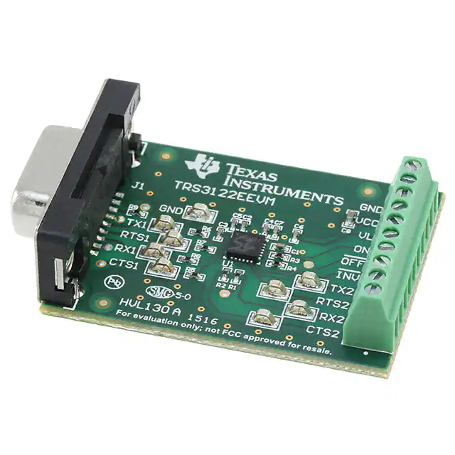
Board Test Points
EVM top view image
The TRS3122EEVM provides test points for all RS-232 (TX1, RTS1, RX1, CTS1) and logic (TX2, RTS2,
RX2, CTS2) communication lines in addition to a ground test point.
4
TRS3122EEVM User's Guide
SLCU001 – May 2016
Submit Documentation Feedback
Copyright © 2016, Texas Instruments Incorporated
�www.ti.com
Printed Circuit Board Layouts
PCB Layout
PCB Layout
PCB Layer Plots
Figure 0-1. Top Layer
Figure 0-2. Bottom Layer
SLCU001 – May 2016
Submit Documentation Feedback
TRS3122EEVM User's Guide
Copyright © 2016, Texas Instruments Incorporated
5
�www.ti.com
Figure 0-3. Top Overlay
Figure 0-4. Top Solder Mask
Figure 0-5. Bottom Solder Mask
Figure 0-6. Drill Drawing
Figure 0-7. Board Dimensions
6
TRS3122EEVM User's Guide
SLCU001 – May 2016
Submit Documentation Feedback
Copyright © 2016, Texas Instruments Incorporated
�www.ti.com
Schematic
TRS3122EEVM Schematic
SLCU001 – May 2016
Submit Documentation Feedback
TRS3122EEVM User's Guide
Copyright © 2016, Texas Instruments Incorporated
7
�www.ti.com
Bill of Materials
Description
!PCB1
1
C1, C2,
C3, C4,
C5, C6,
C7
7
0.1 µF
CAP, CERM, 0.1 µF, 25 V, +/- 10%, X7R,
0402
C8
1
1 µF
J1
Package
Reference
Printed Circuit Board
Part Number
Manufacturer
HVL130
Any
0402
GRM155R71E104K
E14D
MuRata
CAP, CERM, 1 µF, 25 V, +/- 10%, X7R,
0603
0603
GRM188R71E105K
A12
MuRata
1
CONN DB9 FEMALE R/A SOLDER SMD
30.81 x10.28
x10.10 mm
190-009-263R001
NorComp
J2
1
Terminal Block, 10x1, 2.54 mm, TH
Term Block,
10x1, 2.54 mm, 1725737
TH
Phoenix Contact
R1, R2,
R3, R4
4
10.0 k
RES, 10.0 k, 1%, 0.1 W, 0402
0402
ERJ-2RKF1002X
Panasonic
R5, R6,
R7, R8,
R9
5
0
RES, 0, 5%, 0.063 W, 0402
0402
ERJ-2GE0R00X
Panasonic
TP1, TP2,
TP3, TP4,
TP5, TP6,
TP7, TP8
8
SMT
Test Point, Miniature, SMT
Testpoint_Keys
5015
tone_Miniature
Keystone
TP9
1
Test Point, Miniature, SMT
Testpoint_Keys
5015
tone_Miniature
Keystone
U1
1
RS-232 (2 - 2) TRANSCEIVER WITH
SPLIT SUPPLY PIN FOR LOGIC SIDE,
RGE0024H
RGE0024H
TRS3122ERGER
Texas Instruments
FID1,
FID2,
FID3
0
Fiducial mark. There is nothing to buy or
mount.
Fiducial
N/A
N/A
Reference
1. TRS3122E 2Tx/2Rx Low Voltage, Low Power RS232 Transceiver data sheet (SLLSET7)
8
TRS3122EEVM User's Guide
SLCU001 – May 2016
Submit Documentation Feedback
Copyright © 2016, Texas Instruments Incorporated
�IMPORTANT NOTICE
Texas Instruments Incorporated and its subsidiaries (TI) reserve the right to make corrections, enhancements, improvements and other
changes to its semiconductor products and services per JESD46, latest issue, and to discontinue any product or service per JESD48, latest
issue. Buyers should obtain the latest relevant information before placing orders and should verify that such information is current and
complete. All semiconductor products (also referred to herein as “components”) are sold subject to TI’s terms and conditions of sale
supplied at the time of order acknowledgment.
TI warrants performance of its components to the specifications applicable at the time of sale, in accordance with the warranty in TI’s terms
and conditions of sale of semiconductor products. Testing and other quality control techniques are used to the extent TI deems necessary
to support this warranty. Except where mandated by applicable law, testing of all parameters of each component is not necessarily
performed.
TI assumes no liability for applications assistance or the design of Buyers’ products. Buyers are responsible for their products and
applications using TI components. To minimize the risks associated with Buyers’ products and applications, Buyers should provide
adequate design and operating safeguards.
TI does not warrant or represent that any license, either express or implied, is granted under any patent right, copyright, mask work right, or
other intellectual property right relating to any combination, machine, or process in which TI components or services are used. Information
published by TI regarding third-party products or services does not constitute a license to use such products or services or a warranty or
endorsement thereof. Use of such information may require a license from a third party under the patents or other intellectual property of the
third party, or a license from TI under the patents or other intellectual property of TI.
Reproduction of significant portions of TI information in TI data books or data sheets is permissible only if reproduction is without alteration
and is accompanied by all associated warranties, conditions, limitations, and notices. TI is not responsible or liable for such altered
documentation. Information of third parties may be subject to additional restrictions.
Resale of TI components or services with statements different from or beyond the parameters stated by TI for that component or service
voids all express and any implied warranties for the associated TI component or service and is an unfair and deceptive business practice.
TI is not responsible or liable for any such statements.
Buyer acknowledges and agrees that it is solely responsible for compliance with all legal, regulatory and safety-related requirements
concerning its products, and any use of TI components in its applications, notwithstanding any applications-related information or support
that may be provided by TI. Buyer represents and agrees that it has all the necessary expertise to create and implement safeguards which
anticipate dangerous consequences of failures, monitor failures and their consequences, lessen the likelihood of failures that might cause
harm and take appropriate remedial actions. Buyer will fully indemnify TI and its representatives against any damages arising out of the use
of any TI components in safety-critical applications.
In some cases, TI components may be promoted specifically to facilitate safety-related applications. With such components, TI’s goal is to
help enable customers to design and create their own end-product solutions that meet applicable functional safety standards and
requirements. Nonetheless, such components are subject to these terms.
No TI components are authorized for use in FDA Class III (or similar life-critical medical equipment) unless authorized officers of the parties
have executed a special agreement specifically governing such use.
Only those TI components which TI has specifically designated as military grade or “enhanced plastic” are designed and intended for use in
military/aerospace applications or environments. Buyer acknowledges and agrees that any military or aerospace use of TI components
which have not been so designated is solely at the Buyer's risk, and that Buyer is solely responsible for compliance with all legal and
regulatory requirements in connection with such use.
TI has specifically designated certain components as meeting ISO/TS16949 requirements, mainly for automotive use. In any case of use of
non-designated products, TI will not be responsible for any failure to meet ISO/TS16949.
Products
Applications
Audio
www.ti.com/audio
Automotive and Transportation
www.ti.com/automotive
Amplifiers
amplifier.ti.com
Communications and Telecom
www.ti.com/communications
Data Converters
dataconverter.ti.com
Computers and Peripherals
www.ti.com/computers
DLP® Products
www.dlp.com
Consumer Electronics
www.ti.com/consumer-apps
DSP
dsp.ti.com
Energy and Lighting
www.ti.com/energy
Clocks and Timers
www.ti.com/clocks
Industrial
www.ti.com/industrial
Interface
interface.ti.com
Medical
www.ti.com/medical
Logic
logic.ti.com
Security
www.ti.com/security
Power Mgmt
power.ti.com
Space, Avionics and Defense
www.ti.com/space-avionics-defense
Microcontrollers
microcontroller.ti.com
Video and Imaging
www.ti.com/video
RFID
www.ti-rfid.com
OMAP Applications Processors
www.ti.com/omap
TI E2E Community
e2e.ti.com
Wireless Connectivity
www.ti.com/wirelessconnectivity
Mailing Address: Texas Instruments, Post Office Box 655303, Dallas, Texas 75265
Copyright © 2016, Texas Instruments Incorporated
�


 工商网监
湘ICP备2023018690号
工商网监
湘ICP备2023018690号

