Sample &
Buy
Product
Folder
Support &
Community
Tools &
Software
Technical
Documents
TRS3122E
SLLSET7C – MAY 2016 – REVISED MAY 2016
TRS3122E 1.8 V Low Power Dual RS-232 Transceiver
1 Features
3 Description
•
The TRS3122E is a two-driver and two-receiver RS232 interface device, with split supply pins for mixedvoltage operation. All RS-232 inputs and outputs are
protected to ±15 kV using the IEC 61000-4-2 Air-Gap
Discharge method, ±8 kV using the IEC 61000-4-2
Contact Discharge method, and ±15 kV using the
Human-Body Model.
1
•
•
•
•
•
•
•
Extended VCC operating nodes: 1.8 V, 3.3 V, or
5.0 V
– Unique Tripler Charge Pump Architecture
Enables Low VCC of 1.8V While Maintaining
Compatibility with 3.3 V and 5 V Supplies
Integrated Level-Shifting Functionality Eliminates
the Need for External Power or Additional Level
Shifter While Interfacing with Low-Voltage MCUs
Enhanced ESD Protection on RIN Inputs and
DOUT Outputs
– ±15 kV IEC 61000-4-2 Air-Gap Discharge
– ±8 kV IEC 61000-4-2 Contact Discharge
– ±15 kV Human-Body Model
Specified 1000-kbps Data Rate
Auto Powerdown Plus Feature
Low 0.5uA Shutdown Supply Current
Meets or Exceeds Compatibility Requirements of
RS-232 Interface
For 2.5 V Single Supply Applications, Consider
TRS3318E as an Optimized Solution
The charge pump requires five small 0.1-μF
capacitors for operation from as low as a 1.8-V
supply. The TRS3122E is capable of running at data
rates up to 1000 kbps, while maintaining RS-232compatible output levels.
The TRS3122E has a unique VL pin that allows
operation in mixed-logic voltage systems. Both driver
in (DIN) and receiver out (ROUT) logic levels are pin
programmable through the VL pin. This eliminates the
need for additional voltage level shifter while
interfacing with low-voltage microcontrollers or
UARTs.
Auto Powerdown Plus automatically places the
device in a low power mode when the device has not
received or transmitted data for more than 30
seconds. This feature makes this device a very
attractive option for battery powered or other powersensitive applications.
2 Applications
•
•
•
•
•
Remote Radio Unit (RRU)
Base Band Unit (BBU)
Electronic Point of Sale (EPOS)
Diagnostics & Data Transmission
Battery-Powered Equipment
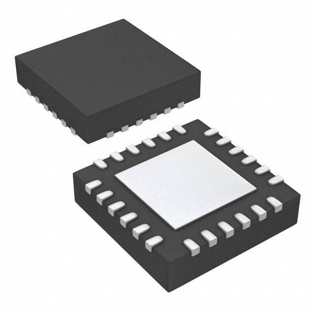
Device Information(1)
PART NUMBER
TRS3122ERGER
PACKAGE (PINS)
RGE (24)
BODY SIZE (NOM)
4.00 mm × 4.00 mm
(1) For all available packages, see the orderable addendum at
the end of the datasheet.
Feature Diagram
Logic Supply
VL
1.8V, 3.3V, 5V
POWER
FORCEON
AUTOPOWERDOWN
PLUS
FORCEOFF
2
DIN
TX
2
DOUT
RS232
1000 kb/s
ROUT
INVALID
2
RX
2
RIN
RS232
STATUS
Copyright © 2016, Texas Instruments Incorporated
1
An IMPORTANT NOTICE at the end of this data sheet addresses availability, warranty, changes, use in safety-critical applications,
intellectual property matters and other important disclaimers. PRODUCTION DATA.
�TRS3122E
SLLSET7C – MAY 2016 – REVISED MAY 2016
www.ti.com
Table of Contents
1
2
3
4
5
6
7
8
Features ..................................................................
Applications ...........................................................
Description .............................................................
Revision History.....................................................
Pin Configuration and Functions .........................
Specifications.........................................................
1
1
1
2
3
4
6.1
6.2
6.3
6.4
6.5
6.6
6.7
6.8
6.9
6.10
6.11
4
4
5
5
5
6
6
6
7
7
8
Absolute Maximum Ratings .....................................
ESD Ratings..............................................................
Recommended Operating Conditions.......................
Thermal Characteristics ............................................
Power and Status Electrical Characteristics .............
Driver Electrical Characteristics ................................
Receiver Electrical Characteristics ...........................
Driver Switching Characteristics ...............................
Receiver Switching Characteristics ..........................
Power and Status Switching Characteristics .........
Typical Characteristics ............................................
Parameter Measurement Information .................. 9
Detailed Description ............................................ 12
8.1
8.2
8.3
8.4
9
Overview .................................................................
Functional Block Diagram .......................................
Feature Description ................................................
Device Functional Modes........................................
12
12
13
15
Application and Implementation ........................ 16
9.1 Application Information............................................ 16
9.2 Typical 1.8-V Application ....................................... 16
10 Power Supply Recommendations ..................... 18
11 Layout................................................................... 19
11.1 Layout Guidelines ................................................. 19
11.2 Layout Example .................................................... 19
12 Device and Documentation Support ................. 20
12.1
12.2
12.3
12.4
12.5
Device Support ....................................................
Community Resources..........................................
Trademarks ...........................................................
Electrostatic Discharge Caution ............................
Glossary ................................................................
20
20
20
20
20
13 Mechanical, Packaging, and Orderable
Information ........................................................... 20
4 Revision History
Changes from Revision B (May 2016) to Revision C
Page
•
Reordered bullets in Features section by priority .................................................................................................................. 1
•
Deleted Data Cables from Applications section of front page to make room for front page image ....................................... 1
•
Changed Corrected swapped ESD levels in description text ................................................................................................. 1
Changes from Revision A (May 2016) to Revision B
Page
•
Updated ESD ratings values to reflect current device specifications .................................................................................... 4
•
Added all Typical Characteristic graphs and schematics to the Typical Characteristics section .......................................... 8
•
Added Application Curve image to Application Curves section .......................................................................................... 18
Changes from Original (June 2014) to Revision A
•
2
Page
Added Pin Functions table. .................................................................................................................................................... 3
Submit Documentation Feedback
Copyright © 2016, Texas Instruments Incorporated
Product Folder Links: TRS3122E
�TRS3122E
www.ti.com
SLLSET7C – MAY 2016 – REVISED MAY 2016
5 Pin Configuration and Functions
18
17
VCC
VL
GND
16
V+
19
C1-
RIN2
15
C1+
20
FORCEON
DOUT1
14
C2+
21
FORCEOFF
13
C2-
22
4
23
5
24
6
V-
VQFN P Package
24-Pin RGE
Top View
INVALID
1
C3-
2
RIN1
3
C3+
(Top View)
DOUT2
11
12
ROUT1
NC
10
ROUT2
NC
9
DIN1
8
DIN2
7
Pin Functions
Pin
NAME
C1+, C2+
NO.
I/O
DESCRIPTION
21, 22
-
Positive terminals of voltage-doubler charge-pump capacitors (required)
1
-
Positive terminal of voltage-tripler charge-pump capacitor (Not needed for VCC 3V to 5.5V)
16, 23
-
Negative terminals of voltage-doubler charge-pump capacitors (required)
C3-
2
-
Negative terminal of voltage-tripler charge-pump capacitor (Not needed for VCC 3V to 5.5V)
V+
20
-
Positive charge pump storage capacitor (required)
V–
24
-
Negative charge pump storage capacitor (required)
GND
17
-
Ground
VCC
19
-
1.8-V or 3-V to 5-V supply voltage
VL
18
-
Logic-level supply. All CMOS inputs (DIN) and outputs (ROUT) are referenced to this supply.
FORCEOFF
14
I
Auto Powerdown Control input (Refer to Truth Table)
FORCEON
15
I
Auto Powerdown Control input (Refer to Truth Table)
INVALID
13
O
Invalid Output Pin
DIN1, DIN2
10,9
I
Driver inputs
DOUT1,
DOUT2
5, 6
O
RS-232 driver outputs
RIN1, RIN2
3, 4
I
RS-232 receiver inputs
12, 11
O
Receiver outputs; swing between 0 and VL
7, 8
I
Factory pins, can be unconnected or connected to GND
C3+
C1–, C2-
ROUT1,
ROUT2
NC
Submit Documentation Feedback
Copyright © 2016, Texas Instruments Incorporated
Product Folder Links: TRS3122E
3
�TRS3122E
SLLSET7C – MAY 2016 – REVISED MAY 2016
www.ti.com
6 Specifications
6.1 Absolute Maximum Ratings (1)
over operating free-air temperature range (unless otherwise noted)
MIN
MAX
VCC
Charge pump power supply
–0.3
6
V
VL
Logic power supply
–0.3
6
V
V+
Positive storage capacitor voltage
–0.3
7
V
V–
Negative storage capacitor voltage
0.3
–7
V
13
V
V+ + |V–|
VI
(2)
Input voltage
FORCEOFF , FORCEON
–0.3
6
DIN
–0.3
VL + 0.3
RIN (0Ω series resistance)
±20
RIN (≥250Ω series resistance)
Output voltage
TJ
Junction temperature
Tstg
Storage temperature range
(1)
(2)
V
±25
DOUT
VO
UNIT
±13.2
ROUT
–0.3
–65
VL + 0.3
V
150
°C
150
°C
Stresses beyond those listed under “absolute maximum ratings” may cause permanent damage to the device. These are stress ratings
only, and functional operation of the device at these or any other conditions beyond those indicated in the operational sections of the
specifications is not implied. Exposure to absolute maximum rating conditions for extended periods may affect device reliability.
V+ and V– can have maximum magnitudes of 7 V, but their absolute difference cannot exceed 13 V.
6.2 ESD Ratings
VALUE
Human body model (HBM), per ANSI/ESDA/JEDEC JS-001,
all pins (1)
V(ESD)
Electrostatic
discharge
Charged device model (CDM), per JEDEC specification
JESD22-C101, all pins (2)
IEC 61000-4-2 Air-Gap Discharge
IEC 61000-4-2 Contact Discharge
(1)
(2)
4
All pins except RS-232 bus
RS-232 bus pins
All pins
RS-232 bus pins
UNIT
±2000
±15000
±500
V
±15000
±8000
JEDEC document JEP155 states that 500-V HBM allows safe manufacturing with a standard ESD control process.
JEDEC document JEP157 states that 250-V CDM allows safe manufacturing with a standard ESD control process.
Submit Documentation Feedback
Copyright © 2016, Texas Instruments Incorporated
Product Folder Links: TRS3122E
�TRS3122E
www.ti.com
SLLSET7C – MAY 2016 – REVISED MAY 2016
6.3 Recommended Operating Conditions
Tripler Mode
VCC
Charge pump power supply
Doubler Mode
MIN
TYP
MAX
1.65
1.8
2
3
3.3
3.6
4.5
5
5.5
UNIT
V
VL
Logic power supply
1.65
VCC
V
RIN
RS-232 Receiver interface
-15
15
V
DOUT
RS-232 Transmitter interface
-12
12
V
VL = 5.0 V
0
1.7
VIL
GPIO Input logic
threshold low
VL = 3.3V
0
1.1
VL = 1.8 V
0
0.6
VL = 5.0V
3.3
VL
VL = 3.3V
2.2
VL
VL = 1.8V
1.2
VL
0
VL
V
–40
85
°C
VIH
VOZ
GPIO Input logic
threshold high
DIN, FORCEOFF, FORCEON
DIN, FORCEOFF, FORCEON
ROUT disabled
FORCEOFF = 0V
Operating temperature
V
V
6.4 Thermal Characteristics
TRS3122E
THERMAL METRIC
UNIT
RGE
RθJA
Junction-to-ambient thermal resistance
34.2
RθJCtop
Junction-to-case (top) thermal resistance
27.2
RθJB
Junction-to-board thermal resistance
11.4
ψJT
Junction-to-top characterization parameter
0.4
ψJB
Junction-to-board characterization parameter
11.4
RθJC(bot)
Junction-to-case (bottom) thermal resistance
3.6
°C/W
6.5 Power and Status Electrical Characteristics
VCC = VL = (1.65 V to 2.0 V) & (3.0V to 5.5V), TA = -40°C to 85°C (unless otherwise noted). Typical data is TA = 25°C, VCC =
VL = 3.3V unless otherwise noted.
PARAMETER
TEST CONDITIONS
DIN1 = GND or VL;
DIN2 = GND or VL,
FORCEOFF = VL
FORCEON = VL
Icc (Static)
Icc (off)
No load
TYP
MAX
VCC= 1.65V to 2.0V
MIN
1.0
1.9
VCC= 3.0V to 3.6V
0.7
1.4
VCC= 4.5V to 5.5V
0.8
1.9
0.4
10
FORCEOFF = GND
VIT+
RIN postive voltage
threshold for INVALID
output change
VIT-
RIN negative voltage
threshold for INVALID
output change
VOH
INVALID high-level
output voltage
IOH = -1 mA, FORCEON = GND, FORCEOFF = VL
VOL
INVALID low-level
output voltage
IOL = 1.6 mA, FORCEON = GND, FORCEOFF = VL
0.3
UNIT
mA
μA
2.4
RIN1 = RIN2
V
-2.4
-0.3
VL-0.4
VL-0.08
VL
V
0
0.06
0.4
V
Submit Documentation Feedback
Copyright © 2016, Texas Instruments Incorporated
Product Folder Links: TRS3122E
5
�TRS3122E
SLLSET7C – MAY 2016 – REVISED MAY 2016
www.ti.com
6.6 Driver Electrical Characteristics
VCC = VL = (1.65 V to 2.0 V) & (3.0V to 5.5V), TA = -40°C to 85°C (unless otherwise noted). Typical data is TA = 25°C, VCC =
VL = 3.3V unless otherwise noted.
PARAMETER
TEST CONDITIONS
VOUT Output voltage swing
MIN
TYP MAX
All driver outputs loaded with 3 kΩ to ground
C3 = 100 nF, VCC= 1.8 V
±4.25
±4.7
All driver outputs loaded with 3 kΩ to ground
C3 = 0 F, VCC= 3.3 V or 5 V
±5
±5.4
300
10M
rO
Output resistance
(VCC = V+ = V– = 0); Driver output = ±2 V
IOS
Output short-circuit
current
VDOUT = 0
IOZ
Output leakage current
VDOUT = ±12 V, FORCEOFF = GND
V
0
Driver input hysteresis
Input leakage current
UNIT
DIN = GND to VL; FORCEOFF = GND to VL; FORCEON = GND to VL
Ω
±60
mA
±25
μA
0.5
1
V
0
±5
μA
6.7 Receiver Electrical Characteristics
VCC = VL = (1.65 V to 2.0 V) & (3.0V to 5.5V), TA = -40°C to 85°C (unless otherwise noted). Typical data is TA = 25°C, VCC =
VL = 3.3V unless otherwise noted.
PARAMETER
TEST CONDITIONS
Ioff
Output leakage current
ROUT, receivers disabled
VOL
Output voltage low
IOUT= 2.0 mA
VOH
Output voltage high
IOUT= –2.0mA
VIT–
VIT+
Vhys
Input threshold low
Input threshold high
TA=25°C
TA =25°C
Input hysteresis
TA=25°C
Input resistance
TA=-40 to 85°C
MIN
TYP
MAX
UNIT
±0.01
±10
μA
0.04
0.3
V
VL–0.3
VL–0.04
VL= 5 V
0.8
1.5
VL= 3.3 V
0.7
1.1
VL= 1.8 V
0.6
0.7
V
V
VL= 5 V
2.0
2.4
VL = 3.3 V
1.5
2.4
VL= 1.8 V
0.9
1.4
VL= 5 V
0.45
VL = 3.3 V
0.35
VL= 1.8 V
V
V
0.26
3
5
7
kΩ
6.8 Driver Switching Characteristics
VCC = VL = (1.65 V to 2.0 V) & (3.0V to 5.5V), TA = -40°C to 85°C (unless otherwise noted). Typical data is TA = 25°C, VCC =
VL = 3.3V unless otherwise noted.
PARAMETER
Maximum data rate
Time-to-exit powerdown
|tPHL – tPLH|
Driver skew
(1)
MIN
RL = 3 kΩ, CL = 500 pF (one driver)
1000
RL = 3 kΩ, CL = 1000 pF (one driver)
500
|VDOUT| > 3.7 V
RL = 3 kΩ
RL = 3 kΩ to 7 kΩ,
T = 25°C
Transition-region slew rate A
Measured from 3 V to –3 V
or –3 V to 3 V
(1)
6
0
TYP
MAX
UNIT
kbps
30
150
μs
50
100
ns
VCC = 1.8V, CL = 200 pF
33
VCC = 1.8V, CL = 1000
pF
25
VCC = 3.3 V, CL = 200 pF
38
VCC = 3.3 V, CL = 1000
pF
28
VCC = 5 V, CL = 200 pF
41
VCC = 5 V, CL = 1000 pF
30
V/μs
Driver skew is measured at the driver zero crosspoint.
Submit Documentation Feedback
Copyright © 2016, Texas Instruments Incorporated
Product Folder Links: TRS3122E
�TRS3122E
www.ti.com
SLLSET7C – MAY 2016 – REVISED MAY 2016
6.9 Receiver Switching Characteristics
VCC = VL = (1.65 V to 2.0 V) & (3.0V to 5.5V), TA = -40°C to 85°C (unless otherwise noted). Typical data is TA = 25°C, VCC =
VL = 3.3V unless otherwise noted.
PARAMETER
TEST CONDITIONS
tPHL
Receiver propagation delay, high to
low
tPLH
Receiver propagation delay, low to
high
tPHL –
tPLH
Receiver skew
ten
Receiver output enable time
tdis
Receiver output disable time
MIN
Receiver input to receiver output
CL = 150 pF
TYP
MAX
UNIT
0.15
0.4
0.15
0.4
50
300
ns
200
400
ns
200
400
ns
μs
From FORCEOFF to ROUT= VL/2
CL = 150 pF, RL = 3 kΩ
6.10 Power and Status Switching Characteristics
VCC = VL = (1.65 V to 2.0 V) & (3.0V to 5.5V), TA = -40°C to 85°C (unless otherwise noted). Typical data is TA = 25°C, VCC =
VL = 3.3V unless otherwise noted.
PARAMETER
MIN
TYP
tvalid
Propagation delay time, low- to high-level output
1
tinvalid
Propagation delay time, high- to low-level output
30
tdis
Receiver or driver edge to auto-powerdown plus
15
30
MAX
μs
μs
60
Submit Documentation Feedback
Copyright © 2016, Texas Instruments Incorporated
Product Folder Links: TRS3122E
UNIT
s
7
�TRS3122E
SLLSET7C – MAY 2016 – REVISED MAY 2016
www.ti.com
6.11 Typical Characteristics
70.0
6
5
4
3
50.0
Driver Output (V)
Supply Current (mA)
60.0
40.0
30.0
20.0
0.0
0.0
1.0
2.0
3.0
4.0
5.0
0.0
0.5
6
5
5
3
2
1.5
2.0
C004
Figure 2. Driver Output vs. Load Capacitance, VCC = 3.3V
VL = 1.8V, RLOAD = 3 kΩ, CH1 = 1 Mbps, CH2 = 32 kbps
6
4
1.0
Load Capacitance (nF)
C005
Driver Positive (V)
Driver Positive (V)
±2
±6
4
3
2
1
1
0
2.75
0
1.6
1.7
1.8
1.9
2.0
2.1
Supply Voltage (V)
45
30
Supply Current (mA)
40
25
1Mbps
500kbps
250kbps
15
1.6
1.7
1.8
1.9
Supply Voltage (V)
2.0
3.75
4.25
4.75
C003
10
1Mbps
500kbps
250kbps
3
4
5
Supply Voltage (V)
C006
Figure 5. Supply Current vs. Supply Voltage (Tripler Mode)
VL = 1.8 V, RLOAD = 3 kΩ, CLOAD = 1 nF, CH2 = 32 kbps
5.75
20
0
2.1
5.25
Figure 4. Driver Positive vs. Supply Voltage (Doubler Mode)
1 Mbps, RLOAD = 3 kΩ, CLOAD = 560 pF
55
35
3.25
Supply Voltage (V)
C002
Figure 3. Driver Positive vs. Supply Voltage (Tripler Mode)
1 Mbps, RLOAD = 3 kΩ, CLOAD = 560 pF
Supply Current (mA)
±1
±5
Figure 1. Supply Current vs. Load Capacitance
VCC = 3.3 V, VL = 1.8 V, RLOAD = 3 kΩ, CH2 = 32 kbps
8
0
±4
6.0
Load Capacitance (nF)
V+
V-
1
±3
Icc 1Mbps
Icc 500kbps
Icc 250kbps
10.0
2
6
C007
Figure 6. Supply Current vs. Supply Voltage (Doubler Mode)
VL = 1.8 V, RLOAD = 3 kΩ, CLOAD = 1 nF, CH2 = 32 kbps
Submit Documentation Feedback
Copyright © 2016, Texas Instruments Incorporated
Product Folder Links: TRS3122E
�TRS3122E
www.ti.com
SLLSET7C – MAY 2016 – REVISED MAY 2016
7 Parameter Measurement Information
VL
FORCEON
VL
Generator
(see Note B)
Input
RS-232
Output
50 Ω
RL
0V
t THL
CL
(see Note A)
FORCEOFF
VL
t TLH
3V
3V
Output
−3 V
−3 V
6V
SR(tr)=
t THL or t TLH
VOH
VOL
VOLTAGE WAVEFORMS
TEST CIRCUIT
A.
CL includes probe and jig capacitance.
B.
The pulse generator has the following characteristics: PRR = 1000 kbit/s, ZO = 50 Ω, 50% duty cycle, tr ≤ 10 ns, tf ≤
10 ns.
Figure 7. Driver Slew Rate
VL
FORCEON
VL
Input
RS-232
Output
Generator
(see Note B)
50 Ω
RL
FORCEOFF
VL
VL /2
VL /2
0V
CL
(see Note A)
t PLH
t PHL
V OH
Driver Skew
tPHL-tPLH
I
I
50%
50%
Output
V OL
VOLTAGE WAVEFORMS
TEST CIRCUIT
A.
CL includes probe and jig capacitance.
B.
The pulse generator has the following characteristics: PRR = 1000 kbit/s, ZO = 50 Ω, 50% duty cycle, tr ≤ 10 ns, tf ≤
10 ns.
Figure 8. Driver Pulse Skew
VL or 0 V
FORCEON
3V
Input
1.5V
1.5 V
−3 V
Output
Generator
(see Note B)
t PHL
50 Ω
VL
FORCEOFF
t PLH
CL
(see Note A)
V OH
50%
Output
50%
V OL
VOLTAGE WAVEFORMS
TEST CIRCUIT
A.
CL includes probe and jig capacitance.
B.
The pulse generator has the following characteristics: ZO = 50 Ω, 50% duty cycle, tr ≤ 10 ns, tf ≤ 10 ns.
Figure 9. Receiver Propagation Delay Times
Submit Documentation Feedback
Copyright © 2016, Texas Instruments Incorporated
Product Folder Links: TRS3122E
9
�TRS3122E
SLLSET7C – MAY 2016 – REVISED MAY 2016
www.ti.com
Parameter Measurement Information (continued)
VL
Input
VL
VL or 0 V
FORCEON
0V
t PHZ
3 V or 0 V
RIN
t PZH
(S1 at GND)
Output
(RIN at 0V)
V OH
50%
Output
CL
(see Note A)
FORCEOFF
0.3 V
t PLZ
(S1 at VL)
50 Ω
VL/2
S1
RL
Generator
(see Note B)
VL/2
GND
t PZL
(RIN at 3V)
0.3 V
VL
Output
50%
V OL
TEST CIRCUIT
VOLTAGE WAVEFORMS
A.
CL includes probe and jig capacitance.
B.
The pulse generator has the following characteristics: ZO = 50 Ω, 50% duty cycle, tr ≤ 10 ns, tf ≤ 10 ns.
C.
tPLZ and tPHZ are the same as tdis.
D.
tPZL and tPZH are the same as ten.
Figure 10. Receiver Enable and Disable Times
10
Submit Documentation Feedback
Copyright © 2016, Texas Instruments Incorporated
Product Folder Links: TRS3122E
�TRS3122E
www.ti.com
SLLSET7C – MAY 2016 – REVISED MAY 2016
Parameter Measurement Information (continued)
Valid RS-232 Level, INVALID High
ROUT
Generator
(see Note B)
2.7 V
50
Indeterminate
0.3 V
0V
If Signal Remains Within This Region
For More Than 30 s, INVALID is Low‚
í0.3 V
Indeterminate
Autopowerdown
Plus
INV ALID
í2.7 V
C L = 30 pF
(see Note A)
Valid RS-232 Level, INVALID High
‚
FORCEOFF
FORCEON
DIN
DOUT
Auto- powerdown plus disables drivers and reduces
supply current to 1 A.
TEST CIRCUIT
Receiver
Input
3V
2.7 V
0 V
0V
í2.7 V
í3 V
tinvalid
tvalid
INV ALID
Output
50%
VL
50%
0V
VL
Driver
Input
50%
50%
0V
VOH
Driver
Output
VOL
tdis
ten
tdis
ten
V+
Supply
V oltages
V+
V+ í0.3 V
Ví +0.3 V
Ví
Ví
Voltage Waveforms and Timing Diagrams
Figure 11. INVALID Propagation-Delay Times and Supply-Enabling Time
Submit Documentation Feedback
Copyright © 2016, Texas Instruments Incorporated
Product Folder Links: TRS3122E
11
�TRS3122E
SLLSET7C – MAY 2016 – REVISED MAY 2016
www.ti.com
8 Detailed Description
8.1 Overview
The TRS3122E is an upgrade to standard RS232 transceivers, offering compatibility with modern system needs
like 1.8-V GPIO capability, enhanced ESD & ultra low stand-by current. The majority of RS-232 transceivers with
1.8-V GPIO compatibility require a logic supply pin for the I/O translation, in addition to a minimum 3.3 V VCC for
all of the other active circuitry on the chip. Unlike these transceivers, TRS3122E can operate with both VL and
VCC equal to 1.8 V. When VCC= 3.0 V to 5.5 V, the charge pump will sense VCC and switch to doubler mode. C1
& C2 are the necessary flying capacitors, C3 is not needed, and the charge pump outputs V+ & V- will regulate
to ~+/-5.4 V. When VCC= 1.65 V to 2.0 V, the charge pump will sense VCC and switch to tripler mode. C1, C2 &
C3 are all necessary, and the charge pump outputs V+ & V- will regulate to ~+/-2.65*VCC from VCC= 1.65 V to 2.0
V.
With many modern applications expanding into products that use RS232 as a backup communication protocol, it
is important for the transceiver to have efficient standby operation. In order to accommodate this, Auto
Powerdown Plus has been integrated to shut-off all active circuitry, allowing TRS3122E to achieve an Ioff of 1 uA.
In order to comply with common interface system needs and environments, the RS-232 receive and transmit I/O
pins comply with IEC 61000-4-2 ratings.
8.2 Functional Block Diagram
1.65V min
CBYPASS
1.65V min
VCC
VL
C1+
V+
C1
C4
Charge Pump
Outputs
C1C2+
V-
C2
C5
C2C3+
C3
C3
FORCEON
FORCEOFF
VL
Auto
Powerdown
INVALID
DOUT1
DIN1
GPIO Inputs
VL
RS232 Outputs
DOUT2
DIN2
RIN1
ROUT1
5NŸ
GPIO Outputs
ROUT2
RS232 Inputs
RIN2
5NŸ
GND
Copyright © 2016, Texas Instruments Incorporated
Figure 12. Schematic
12
Submit Documentation Feedback
Copyright © 2016, Texas Instruments Incorporated
Product Folder Links: TRS3122E
�TRS3122E
www.ti.com
SLLSET7C – MAY 2016 – REVISED MAY 2016
8.3 Feature Description
8.3.1 Charge Pump
The internal power supply consists of a regulated auto-sensing charge pump that provides RS-232 compatible
output voltages, over the 1.65 V to 2.0 V and 3.0 V to 5.5 V VCC ranges. The charge pump operates in two
modes to efficiently accommodate low voltage (1.8 V) and higher voltage (3.3 V & 5.0 V) supplies.
8.3.1.1 Doubler Mode
The charge pump requires two flying capacitors (C1, C2) and reservoir capacitors (C4, C5) to generate the V+
and V- supplies of approximately ±5.4 V when VCC is greater than 3 V. When VCC is >2.9V, TRS3122E will sense
the supply voltage level and switch the charge pump to a doubler. Hence, no need for a third flying capacitor.
C3+ & C3- pins can be left open for proper operation. If a capacitor is placed between C3+ & C3-, the charge
pump will ignore this capacitor and still behave as a doubler.
For capacitor choice recommendations, please refer to Table 1.
8.3.1.2 Tripler Mode
The charge pump requires three flying capacitors (C1, C2 & C3) and reservoir capacitors (C4, C5) to generate
the V+ and V- supplies of approximately ±2.65 * VCC when VCC is greater than 1.65 V. When VCC is


 工商网监
湘ICP备2023018690号
工商网监
湘ICP备2023018690号
