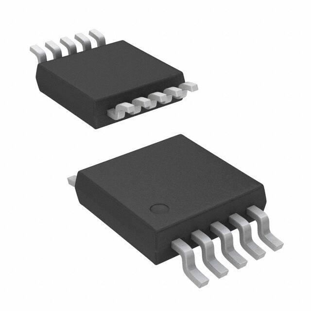
TS5A623157
DUAL 10-Ω SPDT ANALOG SWITCH
WITH UNDERSHOOT/OVERSHOOT VOLTAGE PROTECTION
www.ti.com
SCDS253 – SEPTEMBER 2007
FEATURES
DGS PACKAGE
(TOP VIEW)
1
1
10
NO1
2
9
NC1
GND
3
8
V+
NO2
4
7
NC2
IN2
5
6
COM2
TS5A623157
RSE PACKAGE
(TOP VIEW)
COM1
Sample-and-Hold Circuit
Battery-Powered Equipments
Audio and Video Signal Routing
Communication Circuits
1
NO1
2
GND
3
NO2
4
10
NC1
9
EW
IN1
8
V+
7
NC2
5
6
COM2
IN2
xxx
xxx
DESCRIPTION/ORDERING INFORMATION
The TS5A623157 is a dual single-pole, double-throw (SPDT) analog switch designed to operate from 1.65 V to
5.5 V. This device can handle both digital and analog signals. Signals up to V+ (peak) can be transmitted in
either direction.
The TS5A623157 senses overshoot and undershoot events at the I/Os and responds by preventing voltage
differentials from developing and turning the switch on.
ORDERING INFORMATION
TA
–40°C to 85°C
(1)
(2)
PACKAGE
(1) (2)
ORDERABLE PART NUMBER
TOP-SIDE MARKING
VSSOP (MSOP-10) – DGS
Tape and reel
TS5A623157DGSR
35R
QFN – RSE
Tape and reel
TS5A623157RSER
PREVIEW
Package drawings, thermal data, and symbolization are available at www.ti.com/packaging.
For the most current package and ordering information, see the Package Option Addendum at the end of this document, or see the TI
website at www.ti.com.
FUNCTION TABLE
NC TO COM,
COM TO NC
NO TO COM,
COM TO NO
L
ON
OFF
H
OFF
ON
IN
1
Please be aware that an important notice concerning availability, standard warranty, and use in critical applications of
Texas Instruments semiconductor products and disclaimers thereto appears at the end of this data sheet.
PRODUCT PREVIEW information concerns products in the
formative or design phase of development. Characteristic data and
other specifications are design goals. Texas Instruments reserves
the right to change or discontinue these products without notice.
Copyright © 2007, Texas Instruments Incorporated
PRODUCT PREVIEW
APPLICATIONS
•
•
•
•
COM1
IN1
EV
I
•
Overshoot and Undershoot Voltage Protection
Specified Break-Before-Make Switching
Low ON-State Resistance (10 Ω)
Control Inputs Are 5-V Tolerant
Low Charge Injection
Excellent ON-Resistance Matching
Low Total Harmonic Distortion (THD)
1.8-V to 5.5-V Single-Supply Operation
Latch-Up Performance Exceeds 100 mA Per
JESD 78, Class II
ESD Performance Tested Per JESD 22
– 2000-V Human-Body Model
(A114-B, Class II)
– 1000-V Charged-Device Model (C101)
– 300-V Machine Model (A115-A)
PR
•
•
•
•
•
•
•
•
•
�TS5A623157
DUAL 10-Ω SPDT ANALOG SWITCH
WITH UNDERSHOOT/OVERSHOOT VOLTAGE PROTECTION
www.ti.com
SCDS253 – SEPTEMBER 2007
SUMMARY OF CHARACTERISTICS
V+ = 5 V, TA = 25°C
2:1 multiplexer/demultiplexer (1 × SPDT)
Configuration
Number of channels
2
10 Ω
ON-state resistance (ron)
0.15 Ω
ON-state resistance match (Δron)
2Ω
ON-state resistance flatness (ron(flat))
Turn-on/turn-off time (tON/tOFF)
5 ns / 3.4 ns
Break-before-make time (tBBM)
0.5 ns
Charge injection (QC)
5 pC
Bandwidth (BW)
371 MHz
OFF isolation (OISO)
–61 dB at 10 MHz
Crosstalk (XTALK)
–61 dB at 10 MHz
Total harmonic distortion (THD)
0.06%
Leakage current (INO(OFF)/INC(OFF))
±1 μA
Power-supply current (I+)
1.2 μA
Undershoot protection
–2 V
PRODUCT PREVIEW
Overshoot protection
V+ + 2 V
Package options
10-pin VSSOP (DGS), 10-pin QFN (RSE)
Absolute Minimum and Maximum Ratings (1) (2)
over operating free-air temperature range (unless otherwise noted)
(3)
MIN
MAX
UNIT
–0.5
6.5
V
–0.5
V+ + 0.5
V
V+
Supply voltage range
VNC
VNO
VCOM
Analog voltage range (3) (4) (5)
II/OK
Analog port diode current
V+ < VNC, VNO, VCOM < 0
±50
mA
INC
INO
ICOM
On-state switch current
VNC, VNO, VCOM = 0 to V+
±50
mA
VIN
Digital input voltage range (3) (4)
IIK
Digital input clamp current
I+
IGND
Continuous current through V+ or GND
Tstg
Storage temperature range
(1)
(2)
(3)
(4)
(5)
–0.5
VI < 0
–65
6.5
V
–50
mA
±100
mA
150
°C
Stresses beyond those listed under "absolute maximum ratings" may cause permanent damage to the device. These are stress ratings
only, and functional operation of the device at these or any other conditions beyond those indicated under "recommended operating
conditions" is not implied. Exposure to absolute-maximum-rated conditions for extended periods may affect device reliability.
The algebraic convention, whereby the most negative value is a minimum and the most positive value is a maximum.
All voltages are with respect to ground, unless otherwise specified.
The input and output voltage ratings may be exceeded if the input and output clamp-current ratings are observed.
This value is limited to 5.5 V maximum.
Package Thermal Impedance
UNIT
θJA
(1)
2
Package thermal impedance (1)
DGS package
165
RSE package
243
°C/W
The package thermal impedance is calculated in accordance with JESD 51-7.
Submit Documentation Feedback
Copyright © 2007, Texas Instruments Incorporated
Product Folder Link(s): TS5A623157
�TS5A623157
DUAL 10-Ω SPDT ANALOG SWITCH
WITH UNDERSHOOT/OVERSHOOT VOLTAGE PROTECTION
www.ti.com
SCDS253 – SEPTEMBER 2007
Electrical Characteristics for 5-V Supply
V+ = 4.5 V to 5.5 V, TA = –40°C to 85°C (unless otherwise noted)
PARAMETER
SYMBOL
TEST CONDITIONS
TA
V+
MIN
TYP
MAX
UNIT
Analog Switch
VCOM, VNO,
VNC
0
Voltage
undershoot
VIKU
0 ≥ (INC, INO, or ICOM) ≥ –50 mA
Peak ON-state
resistance
rpeak
0 ≤ (VNO or VNC) ≤ V+,
ICOM = –30 mA,
Switch ON,
See Figure 14
VNO or VNC = 0,
ICOM = 30 mA
ON-state
resistance
ron
5.5 V
25°C
Full
4.6
4.5 V
4
Full
Switch ON,
See Figure 14
VNO or VNC = 4.5 V,
ICOM = –30 mA
25°C
Full
4
4.5 V
VNO or VNC = 3.15 V,
ICOM = –30 mA,
Switch ON,
See Figure 14
ON-state
resistance
flatness
ron(flat)
0 ≤ (VNO or VNC) ≤ V+,
ICOM = –30 mA,
Switch ON,
See Figure 14
NC, NO
OFF leakage
current
INC(OFF),
INO(OFF)
VNC or VNO = 0 to V+,
VCOM = V+ to 0
Switch OFF,
See Figure 15
NC, NO
ON leakage
current
INC(ON),
INO(ON)
VNC or VNO = 0 to V+,
VCOM = Open,
Switch ON,
See Figure 16
10
0.1
0.14
COM
ON leakage
current
ICOM(ON)
VNC or VNO = Open,
VCOM = 0 to V+,
Switch ON,
See Figure 16
1.5
4.5 V
1
5.5 V
1
5.5 V
1
Ω
nA
20
150
5.5 V
Ω
20
150
25°C
Full
Ω
2
4
25°C
Full
8
0.15
25°C
Full
Ω
6.5
5.5
4.5 V
25°C
Full
11
12
25°C
Full
V
10
Full
Δron
–2
8
25°C
ON-state
resistance
match
between
channels
V
13
25°C
VNO or VNC = 2.4 V,
ICOM = –30 mA
V+
PRODUCT PREVIEW
Analog signal
range
nA
20
150
nA
Digital Control Input (IN)
Input logic high
VIH
Full
V+ × 0.7
5.5
V
Input logic low
VIL
Full
0
V+ × 0.3
V
Input leakage
current
IIH, IIL
VI = 5.5 V or 0
25°C
Full
5.5 V
0.1
10
30
Submit Documentation Feedback
Copyright © 2007, Texas Instruments Incorporated
Product Folder Link(s): TS5A623157
nA
3
�TS5A623157
DUAL 10-Ω SPDT ANALOG SWITCH
WITH UNDERSHOOT/OVERSHOOT VOLTAGE PROTECTION
www.ti.com
SCDS253 – SEPTEMBER 2007
Electrical Characteristics for 5-V Supply (continued)
V+ = 4.5 V to 5.5 V, TA = –40°C to 85°C (unless otherwise noted)
PARAMETER
SYMBOL
TEST CONDITIONS
TA
V+
MIN
TYP
MAX
25°C
5V
1
3.5
5
Full
4.5 V to
5.5 V
1
25°C
5V
1
Full
4.5 V to
5.5 V
1
UNIT
Dynamic
Turn-on time
tON
VCOM = V+ or GND,
RL = 500 Ω,
CL = 50 pF,
See Figure 17
Turn-off time
tOFF
VCOM = V+ or GND,
RL = 500 Ω,
CL = 50 pF,
See Figure 17
Output
voltage
during
undershoot
VOUTU
See Figure 24
Output
voltage
during
overshoot
VOUTO
See Figure 24
Break-beforemake time
PRODUCT PREVIEW
Charge
injection
tBBM
QC
2.5
6
2.8
ns
3.4
3.8
VOH – 0.3
ns
V
VOL+ 0.3
2
5
12
V
25°C
5V
0.5
Full
4.5 V to
5.5 V
0.5
CL = 0.1 nF,
See Figure 22
25°C
5V
110
pC
VNC = VNO = V+/2,
RL = 50 Ω,
CL = 50 pF,
See Figure 18
VGEN = 0,
RGEN = 0,
14
ns
NC, NO
OFF
capacitance
CNC(OFF),
CNO(OFF)
VNC or VNO = V+ or
GND,
Switch OFF,
See Figure 16
25°C
5V
5
pF
NC, NO
ON
capacitance
CNC(ON),
CNO(ON)
VNC or VNO = V+ or
GND,
Switch ON,
See Figure 16
25°C
5V
14.5
pF
COM
ON
capacitance
CCOM(ON)
VCOM = V+ or GND,
Switch ON,
See Figure 16
25°C
5V
14.5
pF
Digital input
capacitance
CI
VI = V+ or GND,
See Figure 16
25°C
5V
3.5
pF
Bandwidth
BW
RL = 50 Ω,
Switch ON,
See Figure 19
25°C
5V
371
MHz
OFF isolation
OISO
RL = 50 Ω,
f = 10 MHz,
Switch OFF,
See Figure 20
25°C
5V
–61
dB
Crosstalk
XTALK
RL = 50 Ω,
f = 10 MHz,
Switch ON,
See Figure 21
25°C
5V
–61
dB
Total
harmonic
distortion
THD
RL = 600 Ω,
CL = 50 pF,
f = 20 Hz to
20 kHz,
See Figure 23
25°C
5V
0.06
%
VI = V+ or GND,
Switch ON or
OFF
Supply
Positive supply
current
4
I+
25°C
Full
Submit Documentation Feedback
5.5 V
0.01
0.15
1.2
μA
Copyright © 2007, Texas Instruments Incorporated
Product Folder Link(s): TS5A623157
�TS5A623157
DUAL 10-Ω SPDT ANALOG SWITCH
WITH UNDERSHOOT/OVERSHOOT VOLTAGE PROTECTION
www.ti.com
SCDS253 – SEPTEMBER 2007
Electrical Characteristics for 3.3-V Supply
V+ = 3 V to 3.6 V, TA = –40°C to 85°C (unless otherwise noted)
PARAMETER
SYMBOL
TEST CONDITIONS
TA
V+
MIN
TYP
MAX
UNIT
Analog Switch
VCOM, VNO,
VNC
0
Voltage
undershoot
VIKU
0 ≥ (INC, INO, or ICOM) ≥ –50 mA
Peak ON-state
resistance
rpeak
0 ≤ (VNO or VNC) ≤ V+,
ICOM = –24 mA,
ON-state
resistance
Switch ON,
See Figure 14
ron
VNO or VNC = 3 V,
ICOM = –24 mA
Δron
ON-state
resistance
flatness
3.6 V
25°C
Full
Full
25°C
8.9
3V
5.4
3V
ron(flat)
0 ≤ (VNO or VNC) ≤ V+,
ICOM = –24 mA,
Switch ON,
See Figure 14
NC, NO
OFF leakage
current
INC(OFF),
INO(OFF)
VNC or VNO = 0 to V+,
VCOM = V+ to 0
Switch OFF,
See Figure 15
NC, NO
ON leakage
current
INC(ON),
INO(ON)
VNC or VNO = 0 to V+,
VCOM = Open,
Switch ON,
See Figure 16
COM
ON leakage
current
ICOM(ON)
VNC or VNO = Open,
VCOM = 0 to V+,
Switch ON,
See Figure 16
Full
7.4
12
0.1
0.2
3V
0.2
2.8
3V
0.5
3.6 V
Full
0.5
3.6 V
Full
0.5
3.6 V
nA
10
100
25°C
Ω
10
100
25°C
Ω
4
7
25°C
Full
Ω
15
25°C
Full
Ω
8
10
Full
Switch ON,
See Figure 14
14
18
25°C
VNO or VNC = 2.1 V,
ICOM = –24 mA,
V
V
25°C
VNO or VNC = 0,
ICOM = 24 mA
ON-state
resistance
match
between
channels
Switch ON,
See Figure 14
V+
PRODUCT PREVIEW
Analog signal
range
nA
10
100
nA
Digital Control Input (IN)
Input logic high
VIH
Full
V+ × 0.7
5.5
V
Input logic low
VIL
Full
0
V+ × 0.3
V
Input leakage
current
IIH, IIL
VI = 5.5 V or 0
25°C
Full
3.6 V
0.1
10
20
Submit Documentation Feedback
Copyright © 2007, Texas Instruments Incorporated
Product Folder Link(s): TS5A623157
nA
5
�TS5A623157
DUAL 10-Ω SPDT ANALOG SWITCH
WITH UNDERSHOOT/OVERSHOOT VOLTAGE PROTECTION
www.ti.com
SCDS253 – SEPTEMBER 2007
Electrical Characteristics for 3.3-V Supply (continued)
V+ = 3 V to 3.6 V, TA = –40°C to 85°C (unless otherwise noted)
PARAMETER
SYMBOL
TEST CONDITIONS
TA
V+
MIN
TYP
MAX
4.7
9.0
UNIT
Dynamic
Turn-on time
tON
VCOM = V+ or GND,
RL = 500 Ω,
CL = 50 pF,
See Figure 17
Turn-off time
tOFF
VCOM = V+ or GND,
RL = 500 Ω,
CL = 50 pF,
See Figure 17
PRODUCT PREVIEW
Output voltage
during
undershoot
VOUTU
See Figure 24
Output voltage
during
overshoot
VOUTO
See Figure 24
Break-beforemake time
tBBM
VNC = VNO = V+/2,
RL = 50 Ω,
CL = 50 pF,
See Figure 18
Charge
injection
QC
VGEN = 0,
RGEN = 0,
25°C
3.3 V
1
Full
3 V to
3.6 V
1
25°C
3.3 V
1
Full
3 V to
3.6 V
1
2.5
10.0
3.2
ns
6.3
7.0
VOH – 0.3
ns
V
VOL + 0.3
2
7
17
V
25°C
3.3 V
0.5
Full
3 V to
3.6 V
0.5
CL = 0.1 nF,
See Figure 22
25°C
3.3 V
75
pC
19.5
ns
NC, NO
OFF
capacitance
CNC(OFF),
CNO(OFF)
VNC or VNO = V+ or
GND,
Switch OFF,
See Figure 16
25°C
3.3 V
5
pF
NC, NO
ON capacitance
CNC(ON),
CNO(ON)
VNC or VNO = V+ or
GND,
Switch ON,
See Figure 16
25°C
3.3 V
14.5
pF
COM
ON capacitance
CCOM(ON)
VCOM = V+ or GND,
Switch ON,
See Figure 16
25°C
3.3 V
14.5
pF
VI = V+ or GND,
See Figure 16
25°C
3.3 V
3.5
pF
Digital input
capacitance
CI
Bandwidth
BW
RL = 50 Ω,
Switch ON,
See Figure 19
25°C
3.3 V
370
MHz
OFF isolation
OISO
RL = 50 Ω,
f = 10 MHz,
Switch OFF,
See Figure 20
25°C
3.3 V
–60
dB
Crosstalk
XTALK
RL = 50 Ω,
f = 10 MHz,
Switch ON,
See Figure 21
25°C
3.3 V
–60
dB
Total
harmonic
distortion
THD
RL = 600 Ω,
CL = 50 pF,
f = 20 Hz to
20 kHz,
See Figure 23
25°C
3.3 V
0.1
%
VI = V+ or GND,
Switch ON or
OFF
Supply
Positive
supply
current
6
I+
25°C
Full
0.05
3.6 V
Submit Documentation Feedback
0.5
0.75
μA
Copyright © 2007, Texas Instruments Incorporated
Product Folder Link(s): TS5A623157
�TS5A623157
DUAL 10-Ω SPDT ANALOG SWITCH
WITH UNDERSHOOT/OVERSHOOT VOLTAGE PROTECTION
www.ti.com
SCDS253 – SEPTEMBER 2007
Electrical Characteristics for 2.5-V Supply
V+ = 2.3 V to 2.7 V, TA = –40°C to 85°C (unless otherwise noted)
PARAMETER
SYMBOL
TEST CONDITIONS
TA
V+
MIN
TYP
MAX
UNIT
Analog Switch
VCOM, VNO,
VNC
0
Voltage
undershoot
VIKU
0 mA ≥ (INC, INO, or ICOM) ≥ –50 mA
Peak ON-state
resistance
rpeak
0 ≤ (VNO or VNC) ≤ V+,
ICOM = –8 mA,
ON-state
resistance
Switch ON,
See Figure 14
ron
VNO or VNC = 2.3 V,
ICOM = –8 mA
Δron
ON-state
resistance
flatness
2.7 V
25°C
Full
Full
25°C
13.9
2.3 V
6.6
ron(flat)
0 ≤ (VNO or VNC) ≤ V+,
ICOM = –8 mA,
Switch ON,
See Figure 14
NC, NO
OFF leakage
current
INC(OFF),
INO(OFF)
VNC or VNO = 0 to V+,
VCOM = V+ to 0,
Switch OFF,
See Figure 15
NC, NO
ON leakage
current
INC(ON),
INO(ON)
VNC or VNO = 0 to V+,
VCOM = Open,
Switch ON,
See Figure 16
COM
ON leakage
current
ICOM(ON)
VNC or VNO = Open,
VCOM = 0 to V+,
Switch ON,
See Figure 16
Full
8.9
18
0.05
0.3
2.3 V
0.5
5
2.3 V
0.1
2.7 V
Full
0.1
2.7 V
Full
0.1
2.7 V
nA
10
10
25°C
Ω
10
100
25°C
Ω
15
20
25°C
Full
Ω
25
25°C
Full
Ω
8.5
12
2.3 V
Full
Switch ON,
See Figure 14
30
35
25°C
VNO or VNC = 1.6 V,
ICOM = –8 mA,
V
V
25°C
VNO or VNC = 0,
ICOM = 8 mA
ON-state
resistance
match
between
channels
Switch ON,
See Figure 14
V+
PRODUCT PREVIEW
Analog signal
range
nA
10
100
nA
Digital Control Input (IN)
Input logic high
VIH
Full
V+ × 0.75
5.5
V
Input logic low
VIL
Full
0
V+ × 0.25
V
Input leakage
current
IIH, IIL
VI = 5.5 V or 0
25°C
Full
2.7 V
5
10
20
Submit Documentation Feedback
Copyright © 2007, Texas Instruments Incorporated
Product Folder Link(s): TS5A623157
nA
7
�TS5A623157
DUAL 10-Ω SPDT ANALOG SWITCH
WITH UNDERSHOOT/OVERSHOOT VOLTAGE PROTECTION
www.ti.com
SCDS253 – SEPTEMBER 2007
Electrical Characteristics for 2.5-V Supply (continued)
V+ = 2.3 V to 2.7 V, TA = –40°C to 85°C (unless otherwise noted)
PARAMETER
SYMBOL
TEST CONDITIONS
TA
V+
MIN
TYP
MAX
6.2
9.6
UNIT
Dynamic
Turn-on time
tON
VCOM = V+ or GND,
RL = 500 Ω,
CL = 50 pF,
See Figure 17
Turn-off time
tOFF
VCOM = V+ or GND,
RL = 500 Ω,
CL = 50 pF,
See Figure 17
25°C
2.5 V
2
Full
2.3 V to
2.7 V
2
25°C
2.5 V
1.5
Full
2.3 V to
2.7 V
1.5
12
4.5
7.0
7.5
Output
voltage
during
undershoot
VOUTU
See Figure 24
VOH – 0.3
Output
voltage
during
overshoot
VOUTO
See Figure 24
VOL + 0.3
2
10
25
Break-beforemake time
PRODUCT PREVIEW
Charge
injection
tBBM
QC
ns
ns
V
V
25°C
2.5 V
0.5
Full
2.3 V to
2.7 V
0.5
CL = 0.1 nF,
See Figure 22
25°C
2.5 V
58
pC
VNC = VNO = V+/2,
RL = 50 Ω,
CL = 50 pF,
See Figure 18
VGEN = 0,
RGEN = 0,
28.5
ns
NC, NO
OFF
capacitance
CNC(OFF),
CNO(OFF)
VNC or VNO = V+ or
GND,
Switch OFF,
See Figure 16
25°C
2.5 V
5
pF
NC, NO
ON
capacitance
CNC(ON),
CNO(ON)
VNC or VNO = V+ or
GND,
Switch ON,
See Figure 16
25°C
2.5 V
14.5
pF
COM
ON
capacitance
CCOM(ON)
VCOM = V+ or GND,
Switch ON,
See Figure 16
25°C
2.5 V
14.5
pF
Digital input
capacitance
CI
VI = V+ or GND,
See Figure 16
25°C
2.5 V
3.5
pF
Bandwidth
BW
RL = 50 Ω,
Switch ON,
See Figure 19
25°C
2.5 V
367
MHz
OFF isolation
OISO
RL = 50 Ω,
f = 10 MHz,
Switch OFF,
See Figure 20
25°C
2.5 V
–60
dB
Crosstalk
XTALK
RL = 50 Ω,
f = 10 MHz,
Switch ON,
See Figure 21
25°C
2.5 V
–60
dB
Total
harmonic
distortion
THD
RL = 600 Ω,
CL = 50 pF,
f = 20 Hz to
20 kHz,
See Figure 23
25°C
2.5 V
0.15
%
VI = V+ or GND,
Switch ON or
OFF
Supply
Positive
supply
current
8
I+
25°C
Full
50
2.7 V
Submit Documentation Feedback
100
550
nA
Copyright © 2007, Texas Instruments Incorporated
Product Folder Link(s): TS5A623157
�TS5A623157
DUAL 10-Ω SPDT ANALOG SWITCH
WITH UNDERSHOOT/OVERSHOOT VOLTAGE PROTECTION
www.ti.com
SCDS253 – SEPTEMBER 2007
Electrical Characteristics for 1.8-V Supply
V+ = 1.65 V to 1.95 V, TA = –40°C to 85°C (unless otherwise noted)
PARAMETER
SYMBOL
TEST CONDITIONS
TA
V+
MIN
TYP
MAX
UNIT
Analog Switch
VCOM, VNO,
VNC
0
Voltage
undershoot
VIKU
0 ≥ (INC, INO, or ICOM) ≥ –50 mA
Peak
ON-state
resistance
rpeak
0 ≤ (VNO or VNC) ≤ V+, Switch ON,
ICOM = –4 mA,
See Figure 14
ON-state
resistance
ron
VNO or VNC = 1.65 V,
ICOM = –4 mA
ON-state
resistance
match
between
channels
Δron
ON-state
resistance
flatness
ron(flat)
1.95 V
25°C
Full
Switch ON,
See Figure 14
Full
25°C
41.1
1.65 V
9.2
1.8
0 ≤ (VNO or VNC) ≤ V+, Switch ON,
ICOM = –4 mA,
See Figure 14
NC, NO
OFF leakage
current
INC(OFF),
INO(OFF)
VNC or VNO = 0 to V+,
VCOM = V+ to 0,
Switch OFF,
See Figure 15
NC, NO
ON leakage
current
INC(ON),
INO(ON)
VNC or VNO = 0 to V+,
VCOM = Open,
Switch ON,
See Figure 16
COM
ON leakage
current
ICOM(ON)
VNC or VNO = Open,
VCOM = 0 to V+,
Switch ON,
See Figure 16
Full
0.1
1.65 V
26.5
1.65 V
0.05
1.95 V
0.1
Full
0.1
1.95 V
nA
10
100
25°C
Ω
10
100
1.95 V
Ω
80
100
25°C
Full
Ω
0.6
0.8
25°C
Full
40
45
25°C
Full
Ω
15
15
1.65 V
Full
Switch ON,
See Figure 14
60
120
25°C
VNO or VNC = 1.15 V,
ICOM = –4 mA,
V
V
25°C
VNO or VNC = 0,
ICOM = 4 mA
V+
PRODUCT PREVIEW
Analog signal
range
μA
10
100
nA
Digital Control Input (IN)
Input logic high
VIH
Input logic low
VIL
Input leakage
current
IIH, IIL
VI = 5.5 V or 0
Full
V+ × 0.75
Full
0
25°C
Full
1.95 V
0.05
5.5
V
V+ × 0.25
V
1
20
Submit Documentation Feedback
Copyright © 2007, Texas Instruments Incorporated
Product Folder Link(s): TS5A623157
nA
9
�TS5A623157
DUAL 10-Ω SPDT ANALOG SWITCH
WITH UNDERSHOOT/OVERSHOOT VOLTAGE PROTECTION
www.ti.com
SCDS253 – SEPTEMBER 2007
Electrical Characteristics for 1.8-V Supply (continued)
V+ = 1.65 V to 1.95 V, TA = –40°C to 85°C (unless otherwise noted)
PARAMETER
SYMBOL
TEST CONDITIONS
TA
V+
MIN
TYP
MAX
9.6
23
UNIT
Dynamic
Turn-on time
Turn-off time
tON
VCOM = V+ or GND,
RL = 500 Ω,
CL = 50 pF,
See Figure 17
tOFF
VCOM = V+ or GND,
RL = 500 Ω,
CL = 50 pF,
See Figure 17
25°C
1.8 V
Full
1.65 V
to
1.95 V
25°C
1.8 V
Full
1.65 V
to
1.95 V
24
6.3
ns
10
12
ns
Output
voltage
during
undershoot
VOUTU
See Figure 24
VOH – 0.3
V
Output
voltage
during
overshoot
VOUTO
See Figure 24
VOL + 0.3
V
PRODUCT PREVIEW
Break-beforemake time
Charge
injection
tBBM
QC
25°C
1.8 V
0.5
Full
1.65 V
to
1.95 V
0.5
CL = 0.1 nF,
See Figure 22
25°C
1.8 V
40
pC
VNC = VNO = V+/2,
RL = 50 Ω,
CL = 50 pF,
See Figure 18
VGEN = 0,
RGEN = 0,
18
50
55
ns
NC, NO
OFF
capacitance
CNC(OFF),
CNO(OFF)
VNC or VNO = V+ or
GND,
Switch OFF,
See Figure 16
25°C
1.8 V
5.0
pF
NC, NO
ON
capacitance
CNC(ON),
CNO(ON)
VNC or VNO = V+ or
GND,
Switch ON,
See Figure 16
25°C
1.8 V
14.5
pF
COM
ON
capacitance
CCOM(ON)
VCOM = V+ or GND,
Switch ON,
See Figure 16
25°C
1.8 V
14.5
pF
Digital input
capacitance
CI
VI = V+ or GND,
See Figure 16
25°C
1.8 V
3.5
pF
Bandwidth
BW
RL = 50 Ω,
Switch ON,
See Figure 19
25°C
1.8 V
369
MHz
OFF isolation
OISO
RL = 50 Ω,
f = 10 MHz,
Switch OFF,
See Figure 20
25°C
1.8 V
–60
dB
Crosstalk
XTALK
RL = 50 Ω,
f = 10 MHz,
Switch ON,
See Figure 21
25°C
1.8 V
–60
dB
Total
harmonic
distortion
THD
RL = 600 Ω,
CL = 50 pF,
f = 20 Hz to
20 kHz,
See Figure 23
25°C
1.8 V
0.4
%
VI = V+ or GND,
Switch ON or
OFF
Supply
Positive
supply
current
10
I+
25°C
Full
0.1
1.95 V
Submit Documentation Feedback
50
400
nA
Copyright © 2007, Texas Instruments Incorporated
Product Folder Link(s): TS5A623157
�TS5A623157
DUAL 10-Ω SPDT ANALOG SWITCH
WITH UNDERSHOOT/OVERSHOOT VOLTAGE PROTECTION
www.ti.com
SCDS253 – SEPTEMBER 2007
PIN DESCRIPTION
PIN NO.
NAME
1
IN1
Digital control to connect COM to NO or NC
DESCRIPTION
2
NO1
Normally open
3
GND
Digital ground
4
NO2
Normally open
5
IN2
Digital control to connect COM to NO or NC
6
COM2
7
NC2
8
V+
9
NC1
10
COM1
Common
Normally closed
Power supply
Normally closed
Common
PARAMETER DESCRIPTION
DESCRIPTION
Voltage at COM
VNC
Voltage at NC
VNO
Voltage at NO
ron
Resistance between COM and NC or COM and NO ports when the channel is ON
Δron
Difference of ron between channels
ron(flat)
Difference between the maximum and minimum value of ron in a channel over the specified range of conditions
INC(OFF)
Leakage current measured at the NC port, with the corresponding channel (NC to COM) in the OFF state under
worst-case input and output conditions
INO(OFF)
Leakage current measured at the NO port, with the corresponding channel (NO to COM) in the OFF state under
worst-case input and output conditions
INC(ON)
Leakage current measured at the NC port, with the corresponding channel (NC to COM) in the ON state and the output
(COM) being open
INO(ON)
Leakage current measured at the NO port, with the corresponding channel (NO to COM) in the ON state and the output
(COM) being open
ICOM(ON)
Leakage current measured at the COM port, with the corresponding channel (NO to COM or NC to COM) in the ON state
and the output (NC or NO) being open
VIH
Minimum input voltage for logic high for the control input (IN)
VIL
Minimum input voltage for logic low for the control input (IN)
VIN
Voltage at control input (IN)
IIH, IIL
Leakage current measured at control input (IN)
tON
Turn-on time for the switch. This parameter is measured under the specified range of conditions and by the propagation
delay between the digital control (IN) signal and analog outputs (COM/NC/NO) signal when the switch is turning ON.
tOFF
Turn-off time for the switch. This parameter is measured under the specified range of conditions and by the propagation
delay between the digital control (IN) signal and analog outputs (COM/NC/NO) signal when the switch is turning OFF.
tBBM
Break-before-make time. This parameter is measured under the specified range of conditions and by the propagation
delay between the output of two adjacent analog channels (NC and NO) when the control signal changes state.
QC
Charge injection is a measurement of unwanted signal coupling from the control (IN) input to the analog (NC, NO, or
COM) output. This is measured in coulombs =) and measured by the total charge induced due to switching of the control
input. Charge injection, QC = CL× ΔVO, CL is the load capacitance and ΔVO is the change in analog output voltage.
CNC(OFF)
Capacitance at the NC port when the corresponding channel (NC to COM) is OFF
CNO(OFF)
Capacitance at the NO port when the corresponding channel (NC to COM) is OFF
CNC(ON)
Capacitance at the NC port when the corresponding channel (NC to COM) is ON
CNO(ON)
Capacitance at the NO port when the corresponding channel (NC to COM) is ON
CCOM(ON)
Capacitance at the COM port when the corresponding channel (COM to NC or COM to NO) is ON
CI
Capacitance of control input (IN)
OISO
OFF isolation of the switch is a measurement of OFF-state switch impedance. This is measured in dB in a specific
frequency, with the corresponding channel (NC to COM or NO to COM) in the OFF state.
Submit Documentation Feedback
Copyright © 2007, Texas Instruments Incorporated
Product Folder Link(s): TS5A623157
11
PRODUCT PREVIEW
SYMBOL
VCOM
�TS5A623157
DUAL 10-Ω SPDT ANALOG SWITCH
WITH UNDERSHOOT/OVERSHOOT VOLTAGE PROTECTION
www.ti.com
SCDS253 – SEPTEMBER 2007
PARAMETER DESCRIPTION (continued)
SYMBOL
DESCRIPTION
XTALK
Crosstalk is a measurement of unwanted signal coupling from an ON channel to an OFF channel (NC to NO or NO to
NC). This is measured at a specific frequency and in dB.
BW
Bandwidth of the switch. This is the frequency where the gain of an ON channel is –3 dB below the dc gain.
THD
Total harmonic distortion is defined as the ratio of the root mean square (RMS) value of the second, third, and higher
harmonics to the magnitude of fundamental harmonic.
I+
Static power-supply current with the control (IN) pin at V+ or GND
VOUTU
Output voltage during an undershoot event. This is measured by turning off a specific channel and applying an
undershoot voltage at the input of the switch.
VOUTO
Output voltage during an overshoot event. This is measured by turning off a specific channel and applying an overshoot
voltage at the input of the switch.
PRODUCT PREVIEW
12
Submit Documentation Feedback
Copyright © 2007, Texas Instruments Incorporated
Product Folder Link(s): TS5A623157
�TS5A623157
DUAL 10-Ω SPDT ANALOG SWITCH
WITH UNDERSHOOT/OVERSHOOT VOLTAGE PROTECTION
www.ti.com
SCDS253 – SEPTEMBER 2007
TYPICAL CHARACTERISTICS
12
60
1.8 V
2.5 V
3.3 V
5.0 V
8
30
6
20
4
10
2
0
0.0
0
0
1
2
3
4
–40°C
25°C
85°C
5
0.5
1.0
VCOM (V)
Figure 1. rON vs VCOM
3.5
8
3.0
Leakage Current (nA)
ron (Ω)
2.0
2.5
3.0
Figure 2. rON vs VCOM (V+ = 3.3 V)
9
7
6
5
4
–40°C
25°C
85°C
3
2
2.5
COM (ON)
NC/NO (ON)
NC/NO (OFF)
2.0
1.5
1.0
0.5
1
0.0
0
0
1
2
3
4
–40
5
25
85
TA (°C)
VCOM (V)
Figure 3. rON vs VCOM (V+ = 5 V)
Figure 4. Leakage Current vs Temperature
150
12
100
10
tON/tOFF (ns)
1.8 V
2.5 V
3.3 V
5.0 V
50
QC (pC)
1.5
VCOM (V)
PRODUCT PREVIEW
ron (Ω)
40
10
ron (Ω)
50
0
8
tON
6
tOFF
4
–50
2
–100
0
0
–150
0
1
2
3
Vbias (V)
5
4
Figure 5. Charge Injection vs VCOM
1
2
3
4
5
6
V+ (V)
6
Figure 6. tON and tOFF vs Supply Voltage
Submit Documentation Feedback
Copyright © 2007, Texas Instruments Incorporated
Product Folder Link(s): TS5A623157
13
�TS5A623157
DUAL 10-Ω SPDT ANALOG SWITCH
WITH UNDERSHOOT/OVERSHOOT VOLTAGE PROTECTION
www.ti.com
SCDS253 – SEPTEMBER 2007
TYPICAL CHARACTERISTICS (continued)
2.5
Logic-Level Threshold (V)
4
tON/tOFF (ns)
3
2
tON
tOFF
1
0
–40
25
2.0
1.5
VIN Rising
VIN Falling
1.0
0.5
0.0
85
0
TA (°C)
Figure 7. tON and tOFF vs Temperature
–4
0.25
THD+ (%)
0.30
Gain (db)
–6
–8
1.8 V ±0.35 V
2.5 V ±0.35 V
3.3 V ±0.35 V
5 V ±0.35 V
4
5
6
1.8 V
2.5 V
3.3 V
5.0 V
0.20
0.15
0.10
0.05
0.00
–16
10
–18
0.0E+00 2.0E+08 4.0E+08 6.0E+08 8.0E+08 1.0E+09 1.2E+09
Frequency (Hz)
Figure 9. Bandwidth (BW)
100
1000
10000
Frequency (Hz)
100000
Figure 10. Total Harmonic Distortion (THD) vs Frequency
0
0
–10
-10
–20
-20
–30
-30
1.8 V
2.5 V
3.3 V
5.0 V
–40
–50
–60
–70
Attenuation (dB)
Attenuation (dB)
PRODUCT PREVIEW
–2
–14
3
Figure 8. Logic-Level Threshold
0.35
–12
2
V+ (V)
0
–10
1
-40
-50
-60
1.8 V
2.5 V
3.3 V
5.0 V
-70
-80
–80
-90
–90
0.0E+00 2.0E+08 4.0E+08 6.0E+08 8.0E+08 1.0E+09 1.2E+09
Frequency (Hz)
Figure 11. Off Isolation
14
-100
0.0E+00 2.0E+08 4.0E+08 6.0E+08 8.0E+08 1.0E+09 1.2E+09
Frequency (Hz)
Figure 12. Crosstalk
Submit Documentation Feedback
Copyright © 2007, Texas Instruments Incorporated
Product Folder Link(s): TS5A623157
�TS5A623157
DUAL 10-Ω SPDT ANALOG SWITCH
WITH UNDERSHOOT/OVERSHOOT VOLTAGE PROTECTION
www.ti.com
SCDS253 – SEPTEMBER 2007
TYPICAL CHARACTERISTICS (continued)
0.8
0.7
ICC (μA)
0.6
0.5
0.4
85°C
25°C
–40°C
0.3
0.2
0.1
0.0
–0.1
0.0
1.0
2.0
3.0
4.0
5.0
6.0
VCC (V)
PRODUCT PREVIEW
Figure 13. Supply Current vs Supply Voltage
Submit Documentation Feedback
Copyright © 2007, Texas Instruments Incorporated
Product Folder Link(s): TS5A623157
15
�TS5A623157
DUAL 10-Ω SPDT ANALOG SWITCH
WITH UNDERSHOOT/OVERSHOOT VOLTAGE PROTECTION
www.ti.com
SCDS253 – SEPTEMBER 2007
PARAMETER MEASUREMENT INFORMATION
V+
VNC
NC
VCOM
Channel ON
NO
VNO
COM
r on +
IN
VIN
ICOM
VCOM * VNOńNC
ICOM
W
VIN = VIH or VIL
GND
Figure 14. ON-State Resistance (ron)
V+
PRODUCT PREVIEW
VNC
OFF-State Leakage Current
Channel OFF
VIN = VIH or VIL
VCOM
NC
NO
VNO
COM
ON-State Leakage Current
Channel ON
VIN = VIH or VIL
IN
VIN
VNC or VNO = 0 to V+
or
VCOM = 0 to V+
VNC or VNO = 0 to V+, VCOM = Open
or
VNC or VNO = Open, VCOM = 0 to V+
GND
Figure 15. ON- and OFF-State Leakage Current (ICOM(ON), INC(OFF), INO(OFF), INC(ON), INO(ON))
V+
VCOM
Capacitance
Meter
VBIAS = V+ or GND
VNC
VIN = VIH or VIL
VNO
VBIAS
VIN
Capacitance is measured at NC,
NO, COM, and IN inputs during
ON and OFF conditions.
IN
GND
Figure 16. Capacitance (CIN, CCOM(ON), CNC(OFF), CNO(OFF), CNC(ON), CNO(ON))
16
Submit Documentation Feedback
Copyright © 2007, Texas Instruments Incorporated
Product Folder Link(s): TS5A623157
�TS5A623157
DUAL 10-Ω SPDT ANALOG SWITCH
WITH UNDERSHOOT/OVERSHOOT VOLTAGE PROTECTION
www.ti.com
SCDS253 – SEPTEMBER 2007
PARAMETER MEASUREMENT INFORMATION (continued)
V+
VCOM
(3)
VI
NC or NO
VNC or VNO
NC or NO
CL(2)
TEST
RL
CL
tON
300 Ω
35 pF
tOFF
300 Ω
35 pF
COM
RL
CL(2)
Logic
Input(1)
V+
Logic
Input
(VI)
IN
RL
50%
50%
0
GND
tON
Switch
Output
(VNC or VNO)
tOFF
90%
90%
All input pulses are supplied by generators having the following characteristics: PRR ≤ 10 MHz, ZO = 50 Ω, tr < 5 ns, tf < 5 ns.
CL includes probe and jig capacitance.
(3) See Electrical Characteristic for V
COM.
(1)
PRODUCT PREVIEW
(2)
Figure 17. Turn-On (tON) and Turn-Off (tOFF) Time
tr < 5 ns
tf < 5 ns
V+
VI
NC or NO
COM
RL
CL
IN
Logic
Input
50%
0
NC or NO
VIN
Logic
VIN
Input
VCOM
Switch
Output VCOM
90%
VI = V+/2
RL = 50 Ω
CL = 35 pF
GND
90%
tBBM
Figure 18. Break-Before-Make (tBBM) Time
V+
Network Analyzer
50 W
VNC
Channel ON: NC to COM
NC
COM
Source
Signal
VCOM
Gain + 20 log
NO
50 W
VIN
VCOM
dB
VNC
Network Analyzer Setup
IN
GND
Source Power = 0 dBM
DC Bias = 350 mV
Figure 19. Frequency Response (BW)
Submit Documentation Feedback
Copyright © 2007, Texas Instruments Incorporated
Product Folder Link(s): TS5A623157
17
�TS5A623157
DUAL 10-Ω SPDT ANALOG SWITCH
WITH UNDERSHOOT/OVERSHOOT VOLTAGE PROTECTION
www.ti.com
SCDS253 – SEPTEMBER 2007
PARAMETER MEASUREMENT INFORMATION (continued)
V+
Network Analyzer
50 W
VNC
Channel OFF: NC to COM
NC
COM
Source
Signal
50 W
VCOM
VCOM
dB
VNC
OFF Isolation + 20 log
NO
GND
Network Analyzer Setup
50 W
Source Power = 0 dBM
DC Bias = 350 mV
Figure 20. OFF Isolation (OISO)
V+
Network Analyzer
Channel ON: NC to COM
PRODUCT PREVIEW
50 W
VNC
NC
Channel OFF: NO to COM
VCOM
Source
Signal
Crosstalk + 20 log
NO
VNO
VNO
dB
VNC
50 W
GND
50 W
Network Analyzer Setup
Source Power = 0 dBM
DC Bias = 350 mV
Figure 21. Crosstalk (XTALK)
V+
VINH
Logic
Input
VIN
VINL
RGEN
+
NC or NO
OFF
∆VOUT
VOUT
COM
RL
VIN
ON
VOUT
NC or NO
VGEN
OFF
CL
IN
VGEN = 0
RGEN = 0
RL = 1 MΩ
Logic
Input
CL = 35 pF
QC = CL × ∆VOUT
VIN = VIH or VIL
GND
Figure 22. Charge Injection (QC)
18
Submit Documentation Feedback
Copyright © 2007, Texas Instruments Incorporated
Product Folder Link(s): TS5A623157
�TS5A623157
DUAL 10-Ω SPDT ANALOG SWITCH
WITH UNDERSHOOT/OVERSHOOT VOLTAGE PROTECTION
www.ti.com
SCDS253 – SEPTEMBER 2007
PARAMETER MEASUREMENT INFORMATION (continued)
Channel ON: COM to NC
V+/2
VSOURCE = 0.5 V P-P
V+
10 mF
Analyzer
fSOURCE = 600 Hz to 20 kHz
RL
RL = 600 Ω
NC
CL
CL = 50 pF
10 mF
VO
NO
COM
RL
VSOURCE
GND
Figure 23. Total Harmonic Distortion (THD)
V+
VNC or V NO
RL
VCOM
NC or NO
Switch
Input
NC or NO
COM
RL
CL
IN
VI
Switch Input and Output for Undershoot Test
GND
Switch Input
VNC or V NO
(Open Socket)
90 %
90 %
2 ns
5.5 V
2 ns
10 %
10 %
-2 V
20 ns
TEST
RL
CL
VTR
VOUTU
100 kΩ
10 pF
7V
VOUTO
100 kΩ
10 pF
GND
VI
Switch Output
(VOUTU)
VOH
VOH - 0.3
V+ or GND
Switch OFF
V+ or GND
Switch OFF
Switch Input and Output for Overshoot Test
20 ns
Switch Input
VNC or V NO
(Open Socket)
5.5 V
90 %
90 %
2 ns
10 %
Switch Output
(VOUTO)
2 ns
10 %
VOL + 0.3
VOL
Figure 24. Undershoot and Overshoot Test
Submit Documentation Feedback
Copyright © 2007, Texas Instruments Incorporated
Product Folder Link(s): TS5A623157
19
PRODUCT PREVIEW
VTR
�PACKAGE OPTION ADDENDUM
www.ti.com
6-Feb-2020
PACKAGING INFORMATION
Orderable Device
Status
(1)
TS5A623157DGSR
ACTIVE
Package Type Package Pins Package
Drawing
Qty
VSSOP
DGS
10
2500
Eco Plan
Lead/Ball Finish
MSL Peak Temp
(2)
(6)
(3)
Green (RoHS
& no Sb/Br)
NIPDAU
Level-1-260C-UNLIM
Op Temp (°C)
Device Marking
(4/5)
-40 to 85
35R
(1)
The marketing status values are defined as follows:
ACTIVE: Product device recommended for new designs.
LIFEBUY: TI has announced that the device will be discontinued, and a lifetime-buy period is in effect.
NRND: Not recommended for new designs. Device is in production to support existing customers, but TI does not recommend using this part in a new design.
PREVIEW: Device has been announced but is not in production. Samples may or may not be available.
OBSOLETE: TI has discontinued the production of the device.
(2)
RoHS: TI defines "RoHS" to mean semiconductor products that are compliant with the current EU RoHS requirements for all 10 RoHS substances, including the requirement that RoHS substance
do not exceed 0.1% by weight in homogeneous materials. Where designed to be soldered at high temperatures, "RoHS" products are suitable for use in specified lead-free processes. TI may
reference these types of products as "Pb-Free".
RoHS Exempt: TI defines "RoHS Exempt" to mean products that contain lead but are compliant with EU RoHS pursuant to a specific EU RoHS exemption.
Green: TI defines "Green" to mean the content of Chlorine (Cl) and Bromine (Br) based flame retardants meet JS709B low halogen requirements of


 工商网监
湘ICP备2023018690号
工商网监
湘ICP备2023018690号
