Product
Folder
Sample &
Buy
Technical
Documents
Support &
Community
Tools &
Software
TUSB1210-Q1
SLLSEL4A – SEPTEMBER 2014 – REVISED OCTOBER 2014
TUSB1210-Q1 Standalone USB Transceiver Chip Silicon
1 Features
3 Description
•
The TUSB1210-Q1 is a USB2.0 transceiver chip,
designed to interface with a USB controller via a ULPI
interface. It supports all USB2.0 data rates (HighSpeed 480 Mbps, Full-Speed 12 Mbps and LowSpeed 1.5 Mbps), and is compliant to both Host and
Peripheral modes. It additionally supports a UART
mode and legacy ULPI serial modes.
1
•
•
•
•
•
•
AEC-Q100 Qualified with:
– Temperature Grade 3: –40°C to 85°C
– HBM ESD Classification 1C
– CDM ESD Classification C4B
USB2.0 PHY Transceiver Chip, Designed to
Interface with a USB Controller via a ULPI 12-pin
Interface, Fully Compliant With:
– Universal Serial Bus Specification Rev. 2.0
– On-The-Go Supplement to the USB 2.0
Specification Rev. 1.3
– UTMI+ Low Pin Interface (ULPI) Specification
Rev. 1.1
DP/DM Line External Component Compensation
(Patent #US7965100 B1)
Interfaces to Host, Peripheral and OTG Device
Cores; Optimized for Portable Devices or System
ASICs with Built-in USB OTG Device Core
Complete USB OTG Physical Front-End that
Supports Host Negotiation Protocol (HNP) and
Session Request Protocol (SRP)
ULPI Interface:
– I/O Interface (1.8 V) Optimized for NonTerminated 50 Ω Line Impedance
– ULPI CLOCK Pin (60 MHz) Supports Both
Input and Output Clock Configurations
– Fully Programmable ULPI-Compliant Register
Set
Available in a 32-Pin Quad Flat No Lead
[QFN (RHB)] Package
TUSB1210-Q1 also supports the OTG (Ver1.3)
optional addendum to the USB 2.0 Specification,
including Host Negotiation Protocol (HNP) and
Session Request Protocol (SRP).
The DP/DM external component compensation in the
transmitter compensates for variations in the series
impendence in order to match with the data line
impedance and the receiver input impedance, to limit
data reflections, and thereby, improve eye diagrams.
Device Information(1)
PART NUMBER
TUSB1210-Q1
PACKAGE
BODY SIZE (NOM)
VQFN (32)
5.00 mm x 5.00 mm
(1) For all available packages, see the orderable addendum at
the end of the datasheet.
Diagram
2 Applications
•
•
•
•
•
•
Mobile Phones
Tablet Devices
Desktop Computers
Portable Computers
Video Game Consoles
Portable Music Players
1
An IMPORTANT NOTICE at the end of this data sheet addresses availability, warranty, changes, use in safety-critical applications,
intellectual property matters and other important disclaimers. PRODUCTION DATA.
�TUSB1210-Q1
SLLSEL4A – SEPTEMBER 2014 – REVISED OCTOBER 2014
www.ti.com
Table of Contents
1
2
3
4
5
6
Features ..................................................................
Applications ...........................................................
Description .............................................................
Revision History.....................................................
Pin Configuration and Functions .........................
Specifications.........................................................
6.1
6.2
6.3
6.4
6.5
6.6
6.7
6.8
6.9
6.10
6.11
6.12
6.13
6.14
7
1
1
1
2
3
4
Absolute Maximum Ratings ...................................... 4
Handling Ratings....................................................... 4
Recommended Operating Conditions....................... 5
Thermal Information .................................................. 5
Analog I/O Electrical Characteristics ........................ 5
Digital I/O Electrical Characteristics.......................... 5
Digital IO Pins (Non-ULPI) ....................................... 5
PHY Electrical Characteristics .................................. 6
Pullup/Pulldown Resistors......................................... 8
OTG Electrical Characteristics................................ 9
Power Characteristics ........................................... 10
Switching Characteristics ...................................... 10
Timing Requirements ............................................ 11
Typical Characteristics .......................................... 13
Detailed Description ............................................ 14
7.1 Overview ................................................................. 14
7.2 Functional Block Diagram ....................................... 14
7.3 Feature Description................................................. 15
7.4 Device Functional Modes........................................ 18
7.5 Register Map........................................................... 20
8
Application and Implementation ........................ 49
8.1 Application Information............................................ 49
8.2 Typical Application .................................................. 49
8.3 External Components.............................................. 53
9
Power Supply Recommendations...................... 54
9.1
9.2
9.3
9.4
9.5
TUSB1210 Power Supply .......................................
Ground ....................................................................
Power Providers......................................................
Power Modules .......................................................
Power Consumption................................................
54
54
54
54
55
10 Layout................................................................... 56
10.1 Layout Guidelines ................................................. 56
10.2 Layout Example .................................................... 56
11 Device and Documentation Support ................. 57
11.1
11.2
11.3
11.4
11.5
Documentation Support ........................................
Community Resources..........................................
Trademarks ...........................................................
Electrostatic Discharge Caution ............................
Glossary ................................................................
57
57
57
57
57
12 Mechanical, Packaging, and Orderable
Information ........................................................... 58
12.1 Via Channel........................................................... 58
12.2 Packaging Information .......................................... 58
4 Revision History
Changes from Original (September 2014) to Revision A
Page
•
Changed the Features list ..................................................................................................................................................... 1
•
Deleted 5 paragraphs from the Description following: "TUSB1210-Q1 also supports the OTG (Ver1.3).."........................... 1
•
Changed the Diagram image.................................................................................................................................................. 1
•
Added VIL and VIH to the Recommended Operating Conditions table .................................................................................. 5
•
Changed the Thermal Information table ................................................................................................................................ 5
•
Changed the Digital I/O Electrical Characteristics table ........................................................................................................ 5
•
Digital IO Electrical Characteristics sections to the Switching Characteristics..................................................................... 10
•
Added the Typical Characteristics section............................................................................................................................ 13
•
Added 5 new paragraphs to the Overview section............................................................................................................... 14
2
Submit Documentation Feedback
Copyright © 2014, Texas Instruments Incorporated
Product Folder Links: TUSB1210-Q1
�TUSB1210-Q1
www.ti.com
SLLSEL4A – SEPTEMBER 2014 – REVISED OCTOBER 2014
5 Pin Configuration and Functions
VDDIO
DIR
VDD18
STP
VDD18
RESETB
CLOCK
N/C
32
31
30
29
28
27
26
25
RHB Package
Top View
REFCLK
1
24 N/C
NXT
2
23 ID
DATA0
3
22 VBUS
DATA1
4
21 VBAT
DATA2
5
20 VDD33
DATA3
6
19 DM
DATA4
7
N/C
8
18 DP
GND
14
15
16
CFG
N/C
N/C
12
VDD15
DATA7 13
11
CS
DATA6 10
DATA5
9
17 CPEN
Pin Functions
PIN
NAME
NO.
CFG
14
A/D
TYPE
LEVEL
DESCRIPTION
D
I
VDDIO
REFCLK clock frequency configuration pin. Two frequencies are supported: 19.2 MHz
when 0, or 26 MHz when 1.
ULPI 60 MHz clock on which ULPI data is synchronized.
Two modes are possible:
CLOCK
26
D
O
VDDIO
Input Mode: CLOCK defaults as an input.
Output Mode: When an input clock is detected on REFCLK pin (after 4
rising edges) then CLOCK will change to an output.
CPEN
17
D
O
VDD33
CMOS active-high digital output control of external 5V VBUS supply
CS
11
D
I
VDDIO
Active-high chip select pin. When low the IC is in power down and ULPI bus is tristated. When high normal operation. Tie to VDDIO if unused.
DATA0
3
D
I/O
VDDIO
ULPI DATA input/output signal 0 synchronized to CLOCK
DATA1
4
D
I/O
VDDIO
ULPI DATA input/output signal 1 synchronized to CLOCK
DATA2
5
D
I/O
VDDIO
ULPI DATA input/output signal 2 synchronized to CLOCK
DATA3
6
D
I/O
VDDIO
ULPI DATA input/output signal 3 synchronized to CLOCK
DATA4
7
D
I/O
VDDIO
ULPI DATA input/output signal 4 synchronized to CLOCK
DATA5
9
D
I/O
VDDIO
ULPI DATA input/output signal 5 synchronized to CLOCK
DATA6
10
D
I/O
VDDIO
ULPI DATA input/output signal 6 synchronized to CLOCK
DATA7
13
D
I/O
VDDIO
ULPI DATA input/output signal 7 synchronized to CLOCK
DIR
31
D
O
VDDIO
ULPI DIR output signal
DM
19
A
I/O
VDD33
DM pin of the USB connector
DP
18
A
I/O
VDD33
DP pin of the USB connector
ID
23
A
I/O
VDD33
Identification (ID) pin of the USB connector
N/C
8
–
–
VDDIO
No connect
N/C
15,16, 24,
24
–
–
–
No connect
NXT
2
D
O
VDDIO
ULPI NXT output signal
Submit Documentation Feedback
Copyright © 2014, Texas Instruments Incorporated
Product Folder Links: TUSB1210-Q1
3
�TUSB1210-Q1
SLLSEL4A – SEPTEMBER 2014 – REVISED OCTOBER 2014
www.ti.com
Pin Functions (continued)
PIN
A/D
TYPE
LEVEL
DESCRIPTION
1
A
I
3.3 V
VDD33 Reference clock input (square-wave only). Tie to GND when pin 26 (CLOCK) is
required to be Input mode. Connect to square-wave reference clock of amplitude in
the range of 3 V to 3.6 V when Pin 26 (CLOCK) is required to be Output mode. See
pin 14 (CFG) description for REFCLK input frequency settings.
RESETB
27
D
I
VDDIO
When low, all digital logic (except 32 kHz logic required for power up sequencing)
including registers are reset to their default values, and ULPI bus is tri-stated. When
high, normal USB operation.
NAME
NO.
REFCLK
STP
29
D
I
VDDIO
ULPI STP input signal
VBAT
21
A
power
VBAT
Input supply voltage or battery source
VBUS
22
A
power
VBUS
VBUS pin of the USB connector
VDD15
12
A
power
VDD18
28, 30
A
power
VDD18
External 1.8-V supply input. Connect to external filtering capacitor.
VDD33
20
A
power
VDD33
3.3-V internal LDO output. Connect to external filtering capacitor.
VDDIO
32
A
I
VDDIO
External 1.8V supply input for digital I/Os. Connect to external filtering capacitor.
GND
Thermal
Pad
A
power
--
1.5-V internal LDO output. Connect to external filtering capacitor.
Reference Ground
6 Specifications
6.1 Absolute Maximum Ratings
over operating free-air temperature range (unless otherwise noted) (1)
MIN
MAX
0
5
V
–0.3
1 × VCC +0.3
V
–2
20
V
V
Main battery supply voltage (2)
VCC
Where supply represents the voltage applied
to the power supply pin associated with the
input
Voltage on any input (3)
VBUS input
UNIT
ID, DP, DM inputs
Stress condition specified 24h
–0.3
5.25
VDDIO
IO supply voltage
Continuous
–0.3
1.98
V
TA
Ambient temperature range
–40
85
°C
TJ
Junction temperature range
Ambient temperature for parametric
compliance
DP, DM, ID high voltage short circuit
(1)
(2)
(3)
–40
150
°C
Parametric compliance
–14
125
°C
With max 125°C as junction temperature
–40
85
°C
DP, DM or ID pins short circuited to VBUS
supply, in any mode of TUSB1210-Q1
operation, continuously for 24 hours
0
5.25
V
Stresses beyond those listed under Absolute Maximum Ratings may cause permanent damage to the device. These are stress ratings
only, and functional operation of the device at these or any other conditions beyond those indicated under Recommended Operating
Conditions is not implied. Exposure to absolute-maximum-rated conditions for extended periods may affect device reliability.
The product will have negligible reliability impact if voltage spikes of 5.5 V occur for a total (cumulative over lifetime) duration of 5
milliseconds.
Except VBAT input, VBUS, ID, DP, and DM pads
6.2 Handling Ratings
Tstg
4
MAX
UNIT
–65
150
°C
1500
1500
Corner pins
–750
750
Other pins
–500
500
Storage temperature range
VESD
(1)
MIN
Electrostatic discharge
(ESD) performance:
Human body model (HBM), per AEC Q100-002
Classification Level H1C, all pins (1)
Charged device model (CDM), per AEC
Q100-011 Classification Level C4B
V
AEC Q100-002 indicates HBM stressing is done in accordance with ANSI/ESDA/JEDEC JS-001 specifications.
Submit Documentation Feedback
Copyright © 2014, Texas Instruments Incorporated
Product Folder Links: TUSB1210-Q1
�TUSB1210-Q1
www.ti.com
SLLSEL4A – SEPTEMBER 2014 – REVISED OCTOBER 2014
6.3 Recommended Operating Conditions
over operating free-air temperature range (unless otherwise noted)
PARAMETER
TEST CONDITIONS
Battery supply voltage
VBAT
Battery supply voltage for USB 2.0
compliancy (USB 2.0 certification)
MIN
NOM
MAX
2.7
3.6
4.8
When VDD33 is supplied internally
3.15
When VDD33 is shorted to VBAT externally
3.05
VDDIO
Digital IO pin supply
VIL
Low-level input voltage
CLOCK, STP, DIR, NXT, DATA0 to DATA7
VIH
High-level output voltage
CLOCK, STP, DIR, NXT, DATA0 to DATA7
TA
Ambient temperature range
UNIT
V
V
1.71
1.98
V
0.35 x VDDIO
V
85
°C
0.65 x VDDIO
V
–40
6.4 Thermal Information
RHB
THERMAL METRIC (1)
RθJA
Junction-to-ambient thermal resistance
34.72
RθJC(top)
Junction-to-case(top) thermal resistance
37.3
RθJB
Junction-to-board thermal resistance
10.3
ψJT
Junction-to-top characterization parameter
0.5
ψJB
Junction-to-board characterization parameter
10.5
RθJC(bottom)
Junction-to-case(bottom) thermal resistance
3.6
(1)
UNIT
(16 Pins)
°C/W
For more information about traditional and new thermal metrics, see the IC Package Thermal Metrics application report, SPRA953.
6.5 Analog I/O Electrical Characteristics
over operating free-air temperature range (unless otherwise noted)
PARAMETER
CONDITIONS
MIN
TYP
MAX
UNIT
CPEN Output Pin
VOL
CPEN low-level output voltage
IOL = 3 mA
VOH
CPEN high-level output voltage
IOH = –3 mA
0.3
V
VDD33 – 0.3
V
6.6 Digital I/O Electrical Characteristics
over operating free-air temperature range (unless otherwise noted)
PARAMETER
TEST CONDITIONS
MIN
TYP
MAX
UNIT
0.45
V
CLOCK
VOL
Low-level output voltage
VOH
High-level output voltage
Frequency = 60 MHz, Load = 10 pF
VDDIO - 0.45
V
STP, DIR, NXT, DATA0 to DATA7
VOL
Low-level output voltage
VOH
High-level output voltage
0.45
Frequency = 30 MHz, Load = 10 pF
VDDIO - 0.45
6.7 Digital IO Pins (Non-ULPI)
over operating free-air temperature range (unless otherwise noted)
PARAMETER
TEST CONDITIONS
MIN
TYP
MAX
UNIT
CS, CFG, RESETB Input Pins
VIL
Maximum low-level input voltage
VIH
Minimum high-level input voltage
0.35 x VDDIO
V
0.65 x VDDIO
V
0.2
μs
RESETB Input Pin Timing Spec
tw(POR)
Internal power-on reset pulse
width
Submit Documentation Feedback
Copyright © 2014, Texas Instruments Incorporated
Product Folder Links: TUSB1210-Q1
5
�TUSB1210-Q1
SLLSEL4A – SEPTEMBER 2014 – REVISED OCTOBER 2014
www.ti.com
Digital IO Pins (Non-ULPI) (continued)
over operating free-air temperature range (unless otherwise noted)
PARAMETER
tw(RESET)
External RESETB pulse width
TEST CONDITIONS
MIN
Applied to external RESETB pin
when CLOCK is toggling.
TYP
MAX
UNIT
CLOCK
cycles
8
6.8 PHY Electrical Characteristics
over operating free-air temperature range (unless otherwise noted)
PARAMETER
COMMENTS
MIN
TYP
MAX
–2
0
2
UNIT
LS/FS Single-Ended Receivers
USB single-ended receivers
SKWVP_VM
Skew between VP and VM
VSE_HYS
Single-ended hysteresis
VIH
High (driven)
VIL
Low
VTH
Switching threshold
Driver outputs unloaded
50
2
0.8
ns
mV
V
0.8
V
2
V
LS/FS Differential Receiver
VDI
Differential input sensitivity
Ref. USB2.0
200
VCM
Differential Common mode range
Ref. USB2.0
0.8
mV
VOL
Low
Ref. USB2.0
0
VOH
High (driven)
Ref. USB2.0
2.8
VCRS
Output signal crossover voltage
Ref. USB2.0, covered by eye
diagram
1.3
2
V
tr
Rise time
Ref. USB2.0, covered by eye
diagram
75
300
ns
tf
Fall time
ns
tFRFM
Differential rise and fall time matching
tFDRATE
Low-speed data rate
2.5
V
300
mV
3.6
V
LS Transmitter
tDJ1
Ref. USB2.0, covered by eye
diagram
To next transition
300
125%
1.4775
1.5225
–25
25
–10
10
1.25
1.5
µs
0.8
2.5
V
Mb/s
tDJ2
Source jitter total (including frequency
tolerance)
tFEOPT
Source SE0 interval of EOP
Ref. USB2.0, covered by eye
diagram
Downstream eye diagram
Ref. USB2.0, covered by eye
diagram
Differential common mode range
Ref. USB2.0
VOL
Low
Ref. USB2.0
0
300
mV
VOH
High (driven)
Ref. USB2.0
2.8
3.6
V
VCRS
Output signal crossover voltage
Ref. USB2.0, covered by eye
diagram
1.3
2
V
tFR
Rise time
Ref. USB2.0
4
20
ns
tFF
Fall time
Ref. USB2.0
4
20
ns
tFRFM
Differential rise and fall time matching
Ref. USB2.0, covered by eye
diagram
90%
111.11%
ZDRV
Driver output resistance
Ref. USB2.0
28
44
Full-speed data rate
Ref. USB2.0, covered by eye
diagram
11.97
12.03
–2
2
–1
1
160
175
VCM
For paired
transitions
Ref. USB2.0, covered by eye
diagram
75
80%
ns
FS Transmitter
TFDRATE
tDJ1
To next transition
tDJ2
Source jitter total (including frequency
tolerance)
TFEOPT
Source SE0 interval of EOP
Ref. USB2.0, covered by eye
diagram
Downstream eye diagram
Ref. USB2.0, covered by eye
diagram
6
For paired
transitions
Ref. USB2.0, covered by eye
diagram
Submit Documentation Feedback
Ω
Mb/s
ns
ns
Copyright © 2014, Texas Instruments Incorporated
Product Folder Links: TUSB1210-Q1
�TUSB1210-Q1
www.ti.com
SLLSEL4A – SEPTEMBER 2014 – REVISED OCTOBER 2014
PHY Electrical Characteristics (continued)
over operating free-air temperature range (unless otherwise noted)
PARAMETER
COMMENTS
MIN
TYP
MAX
UNIT
Upstream eye diagram
HS Differential Receiver
VHSSQ
High-speed squelch detection threshold (differential signal
amplitude)
Ref. USB2.0
100
150
mV
VHSDSC
High-speed disconnect detection threshold (differential signal
Ref. USB2.0
amplitude)
525
625
mV
High-speed differential input signaling levels
Ref. USB2.0, specified by eye
pattern templates
High-speed data signaling common mode voltage range
(guidelines for receiver)
Ref. USB2.0
Receiver jitter tolerance
Ref. USB2.0, specified by eye
pattern templates
VHSOI
High-speed idle level
Ref. USB2.0
VHSOH
High-speed data signaling high
Ref. USB2.0
VHSOL
High-speed data signaling low
VCHIRPJ
VCHIRPK
VHSCM
mV
–50
500
mV
150
ps
–10
10
mV
360
440
mV
Ref. USB2.0
–10
10
mV
Chirp J level (differential voltage)
Ref. USB2.0
700
1100
mV
Chirp K level (differential voltage)
Ref. USB2.0
-900
-500
mV
tr
Rise Time (10% - 90%)
Ref. USB2.0, covered by eye
diagram
500
ps
tf
Fall time (10% - 90%)
Ref. USB2.0, covered by eye
diagram
500
ps
ZHSDRV
Driver output resistance (which also serves as high-speed
termination)
Ref. USB2.0
40.5
49.5
THSDRAT
High-speed data range
Ref. USB2.0, covered by eye
diagram
479.76
480.24
Data source jitter
Ref. USB2.0, covered by eye
diagram
Downstream eye diagram
Ref. USB2.0, covered by eye
diagram
Upstream eye diagram
Ref. USB2.0, covered by eye
diagram
HS Transmitter
Ω
Mb/s
CEA-2011/UART Transceiver
UART Transmitter CEA-2011
tPH_UART_EDGE
Phone UART edge rates
DP_PULLDOWN asserted
VOH_SER
Serial interface output high
ISOURCE = 4 mA
VOL_SER
Serial interface output low
1
Μs
2.4
3.3
3.6
V
ISINK = –4 mA
0
0.1
0.4
V
DP_PULLDOWN asserted
2
UART Receiver CEA-2011
VIH_SER
Serial interface input high
VIL_SER
Serial interface input low
VTH
Switching threshold
DP_PULLDOWN asserted
0.8
V
0.8
V
2
V
Submit Documentation Feedback
Copyright © 2014, Texas Instruments Incorporated
Product Folder Links: TUSB1210-Q1
7
�TUSB1210-Q1
SLLSEL4A – SEPTEMBER 2014 – REVISED OCTOBER 2014
www.ti.com
6.9 Pullup/Pulldown Resistors
over operating free-air temperature range (unless otherwise noted)
PARAMETER
COMMENTS
MIN
TYP
MAX
UNIT
0.9
1.1
1.575
kΩ
1.425
2.2
3.09
RPUI
Bus pullup resistor on upstream port
(idle bus)
Bus idle
RPUA
Bus pullup resistor on upstream port
(receiving)
Bus driven/driver's outputs unloaded
VIHZ
High (floating)
Pullups/pulldowns on both DP and
DM lines
VPH_DP_UP
Phone D+ pullup voltage
Driver's outputs unloaded
3
Phone D+/– pulldown
Driver's outputs unloaded
14.25
High (floating)
Pullups/pulldowns on both DP and
DM lines
2.7
3.6
V
3.3
3.6
V
18
24.8
kΩ
3.6
V
75
pF
0.342
V
Pulldown resistors
RPH_DP_DWN
RPH_DM_DWN
VIHZ
2.7
D+/– Data line
CINUB
Upstream facing port
[1.0]
VOTG_DATA_LKG
On-the-go device leakage
[2]
ZINP
Input impedance exclusive of
pullup/pulldown
Driver's outputs unloaded
8
Submit Documentation Feedback
22
300
kΩ
Copyright © 2014, Texas Instruments Incorporated
Product Folder Links: TUSB1210-Q1
�TUSB1210-Q1
www.ti.com
SLLSEL4A – SEPTEMBER 2014 – REVISED OCTOBER 2014
6.10 OTG Electrical Characteristics
over operating free-air temperature range (unless otherwise noted)
PARAMETER
COMMENTS
MIN
TYP
MAX
UNIT
OTG VBUS Electrical
VBUS Comparators
VA_SESS_VLD
A-device session valid
0.8
1.4
2.0
V
VA_VBUS_VLD
A-device VBUS valid
4.4
4.5
4.625
V
VB_SESS_END
B-device session end
0.2
0.5
0.8
V
VB_SESS_VLD
B-device session valid
2.1
2.4
2.7
V
RA_BUS_IN
A-device VBUS input impedance SRP (VBUS pulsing) capable A-device not driving
to ground
VBUS
40
100
kΩ
RB_SRP_DWN
B-device VBUS SRP pulldown
5.25 V / 8 mA, Pullup voltage = 3 V
0.656
10
RB_SRP_UP
B-device VBUS SRP pullup
(5.25 V – 3 V) / 8 mA, Pullup voltage = 3 V
0.281
1
VBUS Line
tRISE_SRP_UP_MAX
B-device VBUS SRP rise time
maximum for OTG-A
communication
0 to 2.1 V with < 13 μF
load
B-device VBUS SRP rise time
minimum for standard host
connection
0.8 to 2 V with > 97 μF
load
kΩ
2
RVBUS = 0 Ω
and R1KSERIES = '0'
31.4
RVBUS = 1000 Ω ±10%
and R1KSERIES = '1'
57.8
RVBUS = 1200 Ω ±10%
and R1KSERIES = '1'
64
RVBUS = 1800 Ω ±10%
and R1KSERIES = '1'
85.4
RVBUS = 0 Ω
and R1KSERIES = '0'
tRISE_SRP_UP_MIN
70
kΩ
ms
46.2
RVBUS = 1000 Ω ±10%
and R1KSERIES = '1'
96
RVBUS = 1200 Ω ±10%
and R1KSERIES = '1'
100
RVBUS = 1800 Ω ±10%
and R1KSERIES = '1'
100
ms
Table 1. OTG ID Electrical
PARAMETER
COMMENTS
MIN
TYP
12
20
MAX
UNIT
ID Comparators — ID External Resistors Specifications
RID_GND
ID ground comparator
ID_GND interrupt
RID_FLOAT
ID Float comparator
ID_FLOAT interrupt
200
28
kΩ
500
kΩ
ID Line
RPH_ID_UP
Phone ID pullup to VPH_ID_UP
ID unloaded (VRUSB)
70
VPH_ID_UP
Phone ID pullup voltage
Connected to VRUSB
2.5
ID line maximum voltage
90
286
kΩ
3.2
V
5.25
V
Submit Documentation Feedback
Copyright © 2014, Texas Instruments Incorporated
Product Folder Links: TUSB1210-Q1
9
�TUSB1210-Q1
SLLSEL4A – SEPTEMBER 2014 – REVISED OCTOBER 2014
www.ti.com
6.11 Power Characteristics
over operating free-air temperature range (unless otherwise noted)
PARAMETER
TEST CONDITIONS
MIN
TYP
MAX
UNIT
VDD33 Internal LDO Regulator Characteristics
VINVDD33
VVDD33
Input voltage
Output voltage
IVDD33
Rated output current
VBAT USB
ON mode,
VBAT USB
VVDD33 typ + 0.2
3.6
4.5
VUSB3V3_VSEL = ‘000
2.4
2.5
2.6
VUSB3V3_VSEL = ‘001
2.65
2.75
2.85
VUSB3V3_VSEL = ‘010
2.9
3.0
3.1
VUSB3V3_VSEL = ‘011 (default)
3.0
3.1
3.2
VUSB3V3_VSEL = ‘100
3.1
3.2
3.3
VUSB3V3_VSEL = ‘101
3.2
3.3
3.4
VUSB3V3_VSEL = ‘110
3.3
3.4
3.5
VUSB3V3_VSEL = ‘111
3.4
3.5
3.6
Active mode
V
V
15
Suspend/reset mode
mA
1
VDD15 Internal LDO Regulator Characteristics
VIN VDD15
Input voltage
On mode, VIN VDD15 = VBAT
2.7
3.6
4.5
V
VVDD15
Output voltage
VINVDD15 min – VINVDD15 max
1.45
1.56
1.65
V
IVDD15
Rated output current
On mode
30
mA
6.12 Switching Characteristics
over operating free-air temperature range (unless otherwise noted)
PARAMETER
TEST CONDITIONS
MIN
TYP
MAX
UNIT
Electrical Characteristics: Clock Input
Clock input duty cycle
fCLK
40
Clock nominal frequency
Clock input rise/fall time
60%
60
In % of clock period tCLK ( = 1/fCLK )
MHz
10%
Clock input frequency accuracy
250
ppm
Clock input integrated jitter
600
ps rms
Electrical Characteristics: REFCLK
REFCLK input duty cycle
fREFCLK
REFCLK nominal frequency
REFCLK input rise/fall time
40
60%
When CFG pin is tied to GND
19.2
When CFG pin is tied to VDDIO
26
In % of clock period tREFCLK ( =
1/fREFCLK )
MHz
20%
REFCLK input frequency accuracy
250
ppm
REFCLK input integrated jitter
600
ps rms
REFCLK HIZ Leakage current
3
REFCLK HIZ Leakage current
–3
µA
Digital IO Electrical Characteristics: CLOCK
tr
Rise time
Frequency = 60 MHz, Load = 10 pF
1
ns
tf
Fall time
Frequency = 30 MHz, Load = 10 pF
1
ns
1
ns
1
ns
Digital IO Electrical Characteristics: STP, DIR, NXT, DATA0 to DATA7
tr
Rise time
tf
Fall time
10
Frequency = 30 MHz, Load = 10 pF
Submit Documentation Feedback
Copyright © 2014, Texas Instruments Incorporated
Product Folder Links: TUSB1210-Q1
�TUSB1210-Q1
www.ti.com
SLLSEL4A – SEPTEMBER 2014 – REVISED OCTOBER 2014
6.13 Timing Requirements
INPUT CLOCK
PARAMETER
MIN
OUTPUT CLOCK
MAX
MIN
MAX
UNIT
ULPI Interface Timing
tSC, tSD
Set-up time (control in, 8-bit data in)
tSC, tHD
Hold time (control in, 8-bit data in)
tDC, tDD
Output delay (control out, 8-bit data out)
3
6
1.5
0
ns
ns
6
9
ns
USB UART Interface Timing
tPH_DP_CON
Phone D+ connect time
100
tPH_DISC_DET
Phone D+ disconnect time
150
fUART_DFLT
Default UART signaling rate (typical rate)
ms
9600
VDDIO, VDD18
bps
ACTIVE
COLDRST
HWRST
OFF
NOPWR
VBAT , VDD33
ms
IORST
CS
TVBBDET (10us)
ICACT
TBGAP (2ms)
BGOK
TPWONVDD15 (100us)
VDD15
DIGPOR
CK32K
TCK32K_PWON (125us)
CK32KOK
TDELRSTPWR (61us)
RESETN_PWR
TDELMNTRVIOEN (91.5us)
TMNTR (183.1us)
MNTR_(VDD18,VIO)_OK
TDELVDD33EN (91.5us)
TMNTR (183.1us)
MNTR_VDD33_OK
(input 60M) CLOCK
RESETB
TDELRESETB (244.1us)
TPLL (300us)
PLL 480M LOCKED
DIR
TDEL_CS_SUPPLYOK (2.84ms)
TDEL_RST_DIR (0.54ms)
Figure 1. TUSB1210-Q1 Power-Up Timing (ULPI Clock Input Mode)
Table 2. Timers and Debounce
TYP
MAX
UNIT
tDEL_CS_SUPPLYOK
Chip-select-to-supplies OK delay
PARAMETER
COMMENTS
MIN
2.84
4.10
ms
tDEL_RST_DIR
RESETB to PHY PLL locked and DIR fallingedge delay
0.54
0.647
ms
tVBBDET
VBAT detection delay
tBGAP
Bandgap power-on delay
tPWONVDD15
tPWONCK32K
tDELRSTPWR
Power control reset delay
tDELMNTRVIOEN
Monitor enable delay
tMNTR
10
µs
2
ms
VDD15 power-on delay
100
µs
32-KHz RC-OSC power-on delay
125
µs
61
µs
91.5
µs
Supply monitoring debounce
183.1
µs
tDELVDD33EN
VDD33 LDO enable delay
93.75
µs
tDELRESETB
RESETB internal delay
244.1
µs
tPLL
PLL lock time
300
µs
Submit Documentation Feedback
Copyright © 2014, Texas Instruments Incorporated
Product Folder Links: TUSB1210-Q1
11
�TUSB1210-Q1
SLLSEL4A – SEPTEMBER 2014 – REVISED OCTOBER 2014
www.ti.com
6.13.1 Timing Parameter Definitions
The timing parameter symbols used in the timing requirement and switching characteristic tables are created in
accordance with JEDEC Standard 100. To shorten the symbols, some pin names and other related terminologies
have been abbreviated as shown in Table 3.
Table 3. Timing Parameter Definitions
LOWERCASE SUBSCRIPTS
SYMBOL
PARAMETER
C
Cycle time (period)
D
Delay time
Dis
Disable time
En
Enable time
H
Hold time
Su
Setup time
START
Start bit
T
Transition time
V
Valid time
W
Pulse duration (width)
X
Unknown, changing, or don't care level
H
High
L
Low
V
Valid
IV
Invalid
AE
Active edge
FE
First edge
LE
Last edge
Z
High impedance
6.13.2 Interface Target Frequencies
Table 4 assumes testing over the recommended operating conditions.
Table 4. TUSB1210-Q1 Interface Target Frequencies
IO
INTERFACE
INTERFACE DESIGNATION
High speed
USB
12
Universal serial bus
TARGET FREQUENCY
1.5 V
480 Mbits/s
Full speed
12 Mbits/s
Low speed
1.5 Mbits/s
Submit Documentation Feedback
Copyright © 2014, Texas Instruments Incorporated
Product Folder Links: TUSB1210-Q1
�TUSB1210-Q1
www.ti.com
SLLSEL4A – SEPTEMBER 2014 – REVISED OCTOBER 2014
6.14 Typical Characteristics
Figure 2. High-Speed Eye Diagram
Figure 3. Full-Speed Eye Diagram
Submit Documentation Feedback
Copyright © 2014, Texas Instruments Incorporated
Product Folder Links: TUSB1210-Q1
13
�TUSB1210-Q1
SLLSEL4A – SEPTEMBER 2014 – REVISED OCTOBER 2014
www.ti.com
7 Detailed Description
7.1 Overview
The TUSB1210-Q1 is a USB2.0 transceiver chip, designed to interface with a USB controller via a ULPI
interface. It supports all USB2.0 data rates High-Speed, Full-Speed, and Low-Speed. Compliant to both Host and
Peripheral (OTG) modes. It additionally supports a UART mode and legacy ULPI serial modes. TUSB1210-Q1
Integrates a 3.3-V LDO, which makes it flexible to work with either battery operated systems or pure 3.3 V
supplied systems. Also, it has an integrated PLL Supporting 2 Clock Frequencies 19.2 MHz/26 MHz. The ULPI
clock pin (60 MHz) supports both input and output clock configurations. TUSB1210-Q1 has low power
consumption, optimized for portable devices, and complete USB OTG Physical Front-End that supports Host
Negotiation Protocol (HNP) and Session Request Protocol (SRP).
TUSB1210-Q1 is optimized to be interfaced through a 12-pin SDR UTMI Low Pin Interface (ULPI), supporting
both input clock and output clock modes, with 1.8 V interface supply voltage.
TUSB1210-Q1 integrates a 3.3 V LDO, which makes it flexible to work with either battery operated systems or
pure 3.3 V supplied systems. Both the main supply and the 3.3 V power domain can be supplied through an
external switched-mode converter for optimized power efficiency.
TUSB1210-Q1 includes a POR circuit to detect supply presence on VBAT and VDDIO pins. TUSB1210-Q1 can be
disabled or configured in low power mode for energy saving.
TUSB1210-Q1 is protected against accidental shorts to 5 V or ground on its exposed interface (DP/DM/ID). It is
also protected against up to 20 V surges on VBUS.
TUSB1210-Q1 integrates a high-performance low-jitter 480 MHz PLL and supports two clock configurations.
Depending on the required link configuration, TUSB1210-Q1 supports both ULPI input and output clock mode :
input clock mode, in which case a square-wave 60 MHz clock is provided to TUSB1210-Q1 at the ULPI interface
CLOCK pin; and output clock mode in which case TUSB1210-Q1 can accept a square-wave reference clock at
REFCLK of either 19.2 MHz, 26 MHz. Frequency is indicated to TUSB1210-Q1 via the configuration pin CFG.
This can be useful if a reference clock is already available in the system.
7.2 Functional Block Diagram
VDDIO (32)
POR
VIO
CTRL
POR
VBAT
VBAT (21)
BGAP
& REF
1V5
POR
DIG
( 1) REFCLK
(11) CS
(14) CFG
(27) RESETB
32K
RST_DIG
VDD15 (12)
DIG
USB-IP
VDD18 (30)
VDD18 (28)
VDD33 (20)
DP (18)
DM (19)
ID (23)
VBUS (22)
1V8
PLL
3V3
OTG
PHY
ANA
PHY
DIG
+
ULPI
+
REGS
PWR_ FSM
( 8) N/C
(15 ) N/C
(16 ) N/C
(25 ) N/C
(24) N /C
OTG
TEST
(17) CPEN
PKG Substrate
(Ground )
(3:7,9:10,13)
DATA(7:0)
(2 ) NXT
(31) DIR
(29) STP
(26) CLOCK
14
Submit Documentation Feedback
Copyright © 2014, Texas Instruments Incorporated
Product Folder Links: TUSB1210-Q1
�TUSB1210-Q1
www.ti.com
SLLSEL4A – SEPTEMBER 2014 – REVISED OCTOBER 2014
7.3 Feature Description
7.3.1 Processor Subsystem
7.3.1.1 Clock Specifications
7.3.1.1.1 USB PLL Reference Clock
The USB PLL block generates the clocks used to synchronize :
• the ULPI interface (60 MHz clock)
• the USB interface (depending on the USB data rate, 480 Mbps, 12 Mbps or 1.5 Mbps)
TUSB1210-Q1 requires an external reference clock which is used as an input to the 480 MHz USB PLL block.
Depending on the clock configuration, this reference clock can be provided either at REFCLK pin or at CLOCK
pin. By default CLK pin is configured as an input.
Two clock configurations are possible:
• Input clock configuration (see ULPI Input Clock Configuration)
• Output clock configuration (see ULPI Output Clock Configuration)
7.3.1.1.2 ULPI Input Clock Configuration
In this mode REFCLK must be externally tied to GND. CLOCK remains configured as an input.
When the ULPI interface is used in input clock configuration, that is, the 60 MHz ULPI clock is provided to
TUSB1210-Q1 on Clock pin, then this is used as the reference clock for the 480 MHz USB PLL block. See
Switching Characteristics.
7.3.1.1.3 ULPI Output Clock Configuration
In this mode a reference clock must be externally provided on REFCLK pin When an input clock is detected on
REFCLK pin then CLK will automatically change to an output, i.e., 60 MHz ULPI clock is output by TUSB1210Q1 on CLK pin.
Two reference clock input frequencies are supported. REFCLK input frequency is communicated to TUSB1210Q1 via a configuration pin, CFG, see fREFCLK in Table 11 for frequency correspondence. TUSB1210-Q1 supports
square-wave reference clock input only. Reference clock input must be square-wave of amplitude in the range 3
V to 3.6 V. See Switching Characteristics.
7.3.1.1.4 Clock 32 kHz
An internal clock generator running at 32 kHz has been implemented to provide a low-speed, low-power clock to
the system See Clock 32 kHz
7.3.1.1.5 Reset
All logic is reset if CS = 0 or VBAT are not present.
All logic (except 32 kHz logic) is reset if VDDIO is not present.
PHY logic is reset when any supplies are not present (VDDIO, VDD15, VDD18, VDD33) or if RESETB pin is low.
TUSB1210-Q1 may be reset manually by toggling the RESETB pin to GND for at lease 200 ns.
If manual reset via RESETB is not required then RESETB pin may be tied to VDDIO permanently.
7.3.1.2 USB Transceiver
The TUSB1210-Q1 device includes a universal serial bus (USB) on-the-go (OTG) transceiver that supports USB
480 Mb/s high-speed (HS), 12 Mb/s full-speed (FS), and USB 1.5 Mb/s low-speed (LS) through a 12-pin UTMI+
low pin interface (ULPI).
Submit Documentation Feedback
Copyright © 2014, Texas Instruments Incorporated
Product Folder Links: TUSB1210-Q1
15
�TUSB1210-Q1
SLLSEL4A – SEPTEMBER 2014 – REVISED OCTOBER 2014
www.ti.com
Feature Description (continued)
NOTE
LS device mode is not allowed by a USB2.0 HS capable PHY, therefore it is not supported
by TUSB1210-Q1. This is stated in USB2.0 standard Chapter 7, page 119, second
paragraph: “A high-speed capable upstream facing transceiver must not support lowspeed signaling mode..” There is also some related commentary in Chapter 7.1.2.3.
7.3.1.2.1 PHY Electrical Characteristics
The PHY is the physical signaling layer of the USB 2.0. It essentially contains all the drivers and receivers
required for physical data and protocol signaling on the DP and DM lines.
The PHY interfaces to the USB controller through a standard 12-pin digital interface called UTMI+ low pin
interface (ULPI).
The transmitters and receivers inside the PHY are classified into two main classes.
• The full-speed (FS) and low-speed (LS) transceivers. These are the legacy USB1.x transceivers.
• The HS (HS) transceivers
In order to bias the transistors and run the logic, the PHY also contains reference generation circuitry which
consists of:
• A DPLL which does a frequency multiplication to achieve the 480-MHz low-jitter lock necessary for USB and
also the clock required for the switched capacitor resistance block.
• A switched capacitor resistance block which is used to replicate an external resistor on chip.
Built-in pullup and pulldown resistors are used as part of the protocol signaling.
Apart from this, the PHY also contains circuitry which protects it from accidental 5-V short on the DP and DM
lines.
7.3.1.2.1.1 LS/FS Single-Ended Receivers
In addition to the differential receiver, there is a single-ended receiver (SE–, SE+) for each of the two data lines
D+/–. The main purpose of the single-ended receivers is to qualify the D+ and D– signals in the full-speed/lowspeed modes of operation. See PHY Electrical Characteristics.
7.3.1.2.1.2 LS/FS Differential Receiver
A differential input receiver (Rx) retrieves the LS/FS differential data signaling. The differential voltage on the line
is converted into digital data by a differential comparator on DP/DM. This data is then sent to a clock and data
recovery circuit which recovers the clock from the data. An additional serial mode exists in which the differential
data is directly output on the RXRCV pin. See Switching Characteristics.
7.3.1.2.1.3 LS/FS Transmitter
The USB transceiver (Tx) uses a differential output driver to drive the USB data signal D+/– onto the USB cable.
The driver's outputs support 3-state operation to achieve bidirectional half-duplex transactions. See Switching
Characteristics.
7.3.1.2.1.4 HS Differential Receiver
The HS receiver consists of the following blocks:
A differential input comparator to receive the serial data
• A squelch detector to qualify the received data
• An oversampler-based clock data recovery scheme followed by a NRZI decoder, bit unstuffing, and serial-toparallel converter to generate the ULPI DATAOUT
See Switching Characteristics.
16
Submit Documentation Feedback
Copyright © 2014, Texas Instruments Incorporated
Product Folder Links: TUSB1210-Q1
�TUSB1210-Q1
www.ti.com
SLLSEL4A – SEPTEMBER 2014 – REVISED OCTOBER 2014
Feature Description (continued)
7.3.1.2.1.5 HS Differential Transmitter
The HS transmitter is always operated via the ULPI parallel interface. The parallel data on the interface is
serialized, bit stuffed, NRZI encoded, and transmitted as a dc output current on DP or DM depending on the
data. Each line has an effective 22.5-Ω load to ground, which generates the voltage levels for signaling.
A disconnect detector is also part of the HS transmitter. A disconnect on the far end of the cable causes the
impedance seen by the transmitter to double thereby doubling the differential amplitude seen on the DP/DM lines
of Switching Characteristics.
7.3.1.2.1.6 UART Transceiver
In this mode, the ULPI data bus is redefined as a 2-pin UART interface, which exchanges data through a direct
access to the FS/LS analog transmitter and receiver. See Switching Characteristics.
Figure 4. USB UART Data Flow
7.3.1.2.2 OTG Characteristics
The on-the-go (OTG) block integrates three main functions:
• The USB plug detection function on VBUS and ID
• The ID resistor detection
• The VBUS level detection
See OTG Electrical Characteristics.
Submit Documentation Feedback
Copyright © 2014, Texas Instruments Incorporated
Product Folder Links: TUSB1210-Q1
17
�TUSB1210-Q1
SLLSEL4A – SEPTEMBER 2014 – REVISED OCTOBER 2014
www.ti.com
7.4 Device Functional Modes
7.4.1 TUSB1210-Q1 Modes vs ULPI Pin Status
Table 5, Table 6, and Table 7 show the status of each of the 12 ULPI pins including input/output direction and
whether output pins are driven to ‘0’ or to ‘1’, or pulled up/pulled down via internal pullup/pulldown resistors.
Note that pullup/pulldown resistors are automatically replaced by driven ‘1’/’0’ levels respectively once internal
IORST is released, with the exception of the pullup on STP which is maintained in all modes.
Pin assignment changes in ULPI 3-pin serial mode, ULPI 6-pin serial mode, and UART mode. Unused pins are
tied low in these modes as shown below.
Table 5. TUSB1210-Q1 Modes vs ULPI Pin Status:ULPI Synchronous Mode Power-Up
ULPI SYNCHRONOUS MODE POWER-UP
UNTIL IORST RELEASE
PIN
NO.
PIN NAME
DIR
PU/PD
26
CLOCK
Hiz
31
DIR
Hiz
PLL OFF
PLL ON + STP HIGH
DIR
PU/PD
PD
I
PU
O, (‘1’)
PLL ON + STP LOW
DIR
PU/PD
DIR
PU/PD
PD
IO
-
IO
-
-
O, (‘0’)
-
O
-
2
NXT
Hiz
PD
O, (‘0’)
-
O, (‘0’)
-
O
-
29
STP
Hiz
PU
I
PU
I
PU
I
PU
3
DATA0
Hiz
PD
O, (‘0’)
-
I
PD
IO
-
4
DATA1
Hiz
PD
O, (‘0’)
-
I
PD
IO
-
5
DATA2
Hiz
PD
O, (‘0’)
-
I
PD
IO
-
6
DATA3
Hiz
PD
O, (‘0’)
-
I
PD
IO
-
7
DATA4
Hiz
PD
O, (‘0’)
-
I
PD
IO
-
9
DATA5
Hiz
PD
O, (‘0’)
-
I
PD
IO
-
10
DATA6
Hiz
PD
O, (‘0’)
-
I
PD
IO
-
13
DATA7
Hiz
PD
O, (‘0’)
-
I
PD
IO
-
Table 6. TUSB1210-Q1 Modes vs ULPI Pin Status: USB Suspend Mode
LINK / EXTERNAL RECOMMENDED SETTING DURING
SUSPEND MODE
SUSPEND MODE
(1)
18
PIN NO.
PIN NAME
DIR
PU/PD
DIR
PU/PD
26
CLOCK
I
-
O
-
31
DIR
O, (‘1’)
-
I
-
2
NXT
O, (‘0’)
-
I
-
29
STP
I
PU (1)
O, (‘0’)
-
3
DATA0
O, (LINESTATE0)
-
I
-
4
DATA1
O, (LINESTATE1)
-
I
-
5
DATA2
O, (‘0’)
-
I
-
6
DATA3
O, (INT)
-
I
-
7
DATA4
O, (‘0’)
-
I
-
9
DATA5
O, (‘0’)
-
I
-
10
DATA6
O, (‘0’)
-
I
-
13
DATA7
O, (‘0’)
-
I
-
Can be disabled by software before entering Suspend Mode to reduce current consumption
Submit Documentation Feedback
Copyright © 2014, Texas Instruments Incorporated
Product Folder Links: TUSB1210-Q1
�TUSB1210-Q1
www.ti.com
SLLSEL4A – SEPTEMBER 2014 – REVISED OCTOBER 2014
Table 7. TUSB1210-Q1 Modes vs ULPI Pin Status: ULPI 6-Pin Serial Mode and UART Mode
ULPI 6-PIN SERIAL MODE
ULPI 3-PIN SERIAL MODE
UART MODE
PIN NO.
PIN NAME
DIR
PU/PD
PIN NAME
DIR
PU/PD
PIN NAME
DIR
PU/PD
26
CLOCK (1)
IO
-
CLOCK (1)
IO
-
CLOCK (1)
IO
-
31
DIR
O
-
DIR
O
-
DIR
O
-
2
NXT
O
-
NXT
O
-
NXT
O
-
29
STP
I
PU
STP
I
PU
STP
I
PU
3
TX_ENABLE
I
-
TX_ENABLE
I
-
TXD
I
-
4
TX_DAT
I
-
DAT
IO
-
RXD
IO
-
5
TX_SE0
I
-
SE0
IO
-
tie low
O
-
6
INT
O
-
INT
O
-
INT
O
-
7
RX_DP
O
-
tie low
O
-
tie low
O
-
9
RX_DM
O
-
tie low
O
-
tie low
O
-
10
RX_RCV
O
-
tie low
O
-
tie low
O
13
tie low
O
-
tie low
O
-
tie low
O
-
Submit Documentation Feedback
Copyright © 2014, Texas Instruments Incorporated
Product Folder Links: TUSB1210-Q1
19
�TUSB1210-Q1
SLLSEL4A – SEPTEMBER 2014 – REVISED OCTOBER 2014
www.ti.com
7.5 Register Map
Table 8. USB Register Summary
20
REGISTER NAME
TYPE
REGISTER WIDTH (BITS)
PHYSICAL ADDRESS
VENDOR_ID_LO
R
8
0x00
VENDOR_ID_HI
R
8
0x01
PRODUCT_ID_LO
R
8
0x02
PRODUCT_ID_HI
R
8
0x03
FUNC_CTRL
RW
8
0x04
FUNC_CTRL_SET
RW
8
0x05
FUNC_CTRL_CLR
RW
8
0x06
IFC_CTRL
RW
8
0x07
IFC_CTRL_SET
RW
8
0x08
IFC_CTRL_CLR
RW
8
0x09
OTG_CTRL
RW
8
0x0A
OTG_CTRL_SET
RW
8
0x0B
OTG_CTRL_CLR
RW
8
0x0C
USB_INT_EN_RISE
RW
8
0x0D
USB_INT_EN_RISE_SET
RW
8
0x0E
USB_INT_EN_RISE_CLR
RW
8
0x0F
USB_INT_EN_FALL
RW
8
0x10
USB_INT_EN_FALL_SET
RW
8
0x11
USB_INT_EN_FALL_CLR
RW
8
0x12
USB_INT_STS
R
8
0x13
USB_INT_LATCH
R
8
0x14
DEBUG
R
8
0x15
SCRATCH_REG
RW
8
0x16
SCRATCH_REG_SET
RW
8
0x17
SCRATCH_REG_CLR
RW
8
0x18
Reserved
R
8
0x19 0x2E
ACCESS_EXT_REG_SET
RW
8
0x2F
Reserved
R
8
0x30 0x3C
VENDOR_SPECIFIC1
RW
8
0x3D
VENDOR_SPECIFIC1_SET
RW
8
0x3E
VENDOR_SPECIFIC1_CLR
RW
8
0x3F
VENDOR_SPECIFIC2
RW
8
0x80
VENDOR_SPECIFIC2_SET
RW
8
0x81
VENDOR_SPECIFIC2_CLR
RW
8
0x82
VENDOR_SPECIFIC1_STS
R
8
0x83
VENDOR_SPECIFIC1_LATCH
R
8
0x84
VENDOR_SPECIFIC3
RW
8
0x85
VENDOR_SPECIFIC3_SET
RW
8
0x86
VENDOR_SPECIFIC3_CLR
RW
8
0x87
Submit Documentation Feedback
Copyright © 2014, Texas Instruments Incorporated
Product Folder Links: TUSB1210-Q1
�TUSB1210-Q1
www.ti.com
SLLSEL4A – SEPTEMBER 2014 – REVISED OCTOBER 2014
7.5.1 VENDOR_ID_LO
ADDRESS OFFSET
0x00
PHYSICAL ADDRESS
0x00
DESCRIPTION
Lower byte of vendor ID supplied by USB-IF (TI Vendor ID = 0x0451)
TYPE
R
INSTANCE
USB_SCUSB
WRITE LATENCY
7
6
5
4
3
2
1
0
VENDOR_ID
BITS
FIELD NAME
7:00
VENDOR_ID
DESCRIPTION
TYPE
RESET
R
0x51
7.5.2 VENDOR_ID_HI
ADDRESS OFFSET
0x01
PHYSICAL ADDRESS
0x01
DESCRIPTION
Upper byte of vendor ID supplied by USB-IF (TI Vendor ID = 0x0451)
TYPE
R
INSTANCE
USB_SCUSB
WRITE LATENCY
7
6
5
4
3
2
1
0
VENDOR_ID
BITS
FIELD NAME
7:00
VEN DOR_ID
DESCRIPTION
TYPE
RESET
R
0x04
7.5.3 PRODUCT_ID_LO
ADDRESS OFFSET
0x02
PHYSICAL ADDRESS
0x02
DESCRIPTION
Lower byte of Product ID supplied by Vendor (TUSB1210-Q1 Product ID is 0x1507).
TYPE
R
INSTANCE
USB_SCUSB
WRITE LATENCY
7
6
5
4
3
2
1
0
PRODUCT_ID
BITS
FIELD NAME
7:00
DESCRIPTION
PRODUCT_ID
TYPE
RESET
R
0x07
Submit Documentation Feedback
Copyright © 2014, Texas Instruments Incorporated
Product Folder Links: TUSB1210-Q1
21
�TUSB1210-Q1
SLLSEL4A – SEPTEMBER 2014 – REVISED OCTOBER 2014
www.ti.com
7.5.4 PRODUCT_ID_HI
ADDRESS OFFSET
0x03
PHYSICAL ADDRESS
0x03
DESCRIPTION
Upper byte of Product ID supplied by Vendor (TUSB1210-Q1 Product ID is 0x1507).
TYPE
R
INSTANCE
USB_SCUSB
WRITE LATENCY
7
6
5
4
3
2
1
0
PRODUCT_ID
BITS
FIELD NAME
7:00
DESCRIPTION
TYPE
RESET
R
0x15
PRODUCT_ID
7.5.5 FUNC_CTRL
ADDRESS OFFSET
0x04
PHYSICAL ADDRESS
0x04
DESCRIPTION
Controls UTMI function settings of the PHY.
TYPE
RW
INSTANCE
USB_SCUSB
WRITE LATENCY
7
6
5
Reserved
SUSPENDM
RESET
BITS
4
3
OPMODE
FIELD NAME
2
1
TERMSELECT
0
XCVRSELECT
DESCRIPTION
TYPE
RESET
7
Reserved
R
0
6
SUSPENDM
Active low PHY suspend. Put PHY into Low Power Mode. In Low Power
Mode the PHY power down all blocks except the full speed receiver, OTG
comparators, and the ULPI interface pins. The PHY automatically set this bit
to '1' when Low Power Mode is exited.
RW
1
5
RESET
Active high transceiver reset. Does not reset the ULPI interface or ULPI
register set.
RW
0
RW
0x0
Once set, the PHY asserts the DIR signal and reset the UTMI core. When the
reset is completed, the PHY de-asserts DIR and clears this bit. After deasserting DIR, the PHY re-assert DIR and send an RX command update.
Note: This bit is auto-cleared, this explain why it can't be read at '1'.
4:03
OPMODE
Select the required bit encoding style during transmit
0x0:
Normal operation
0x1:
Non-driving
0x2:
Disable bit-stuff and NRZI encoding
0x3:
Reserved (No SYNC and EOP generation feature not supported)
2
TERMSELECT
Controls the internal 1.5Kohms pull-up resistor and 45ohms HS terminations.
Control over bus resistors changes depending on XcvrSelect, OpMode,
DpPulldown and DmPulldown.
RW
0
1:00
XCVRSELECT
Select the required transceiver speed.
RW
0x1
0x0:
Enable HS transceiver
0x1:
Enable FS transceiver
0x2:
Enable LS transceiver
0x3:
Enable FS transceiver for LS packets
(FS preamble is automatically pre-pended)
7.5.6 FUNC_CTRL_SET
ADDRESS OFFSET
0x05
PHYSICAL ADDRESS
0x05
22
INSTANCE
Submit Documentation Feedback
USB_SCUSB
Copyright © 2014, Texas Instruments Incorporated
Product Folder Links: TUSB1210-Q1
�TUSB1210-Q1
www.ti.com
SLLSEL4A – SEPTEMBER 2014 – REVISED OCTOBER 2014
DESCRIPTION
This register doesn't physically exist.
It is the same as the func_ctrl register with read/set-only property (write '1' to set a particular bit, a write
'0' has no-action).
TYPE
RW
WRITE LATENCY
7
6
5
Reserved
SUSPENDM
RESET
4
3
OPMODE
2
1
TERMSELECT
DESCRIPTION
0
XCVRSELECT
BITS
FIELD NAME
TYPE
RESET
7
Reserved
R
0
6
SUSPENDM
RW
1
5
RESET
RW
0
4:03
OPMODE
RW
0x0
2
TERMSELECT
RW
0
1:00
XCVRSELECT
RW
0x1
7.5.7 FUNC_CTRL_CLR
ADDRESS OFFSET
0x06
PHYSICAL ADDRESS
0x06
DESCRIPTION
This register doesn't physically exist.
INSTANCE
USB_SCUSB
It is the same as the func_ctrl register with read/clear-only property (write '1' to clear a particular bit, a
write '0' has no-action).
TYPE
RW
WRITE LATENCY
7
6
5
Reserved
SUSPENDM
RESET
4
3
OPMODE
DESCRIPTION
2
1
TERMSELECT
0
XCVRSELECT
BITS
FIELD NAME
TYPE
RESET
7
Reserved
R
0
6
SUSPENDM
RW
1
5
RESET
RW
0
4:03
OPMODE
RW
0x0
2
TERMSELECT
RW
0
1:00
XCVRSELECT
RW
0x1
Submit Documentation Feedback
Copyright © 2014, Texas Instruments Incorporated
Product Folder Links: TUSB1210-Q1
23
�TUSB1210-Q1
SLLSEL4A – SEPTEMBER 2014 – REVISED OCTOBER 2014
www.ti.com
7.5.8 IFC_CTRL
ADDRESS OFFSET
0x07
PHYSICAL ADDRESS
0x07
DESCRIPTION
Enables alternative interfaces and PHY features.
TYPE
RW
INSTANCE
USB_SCUSB
WRITE LATENCY
7
6
5
4
3
INTERFACE_P
INDICATORPA INDICATORCO
CLOCKSUSPE
ROTECT_DISA
AUTORESUME
SSTHRU
MPLEMENT
NDM
BLE
BITS
7
FIELD NAME
2
CARKITMODE
1
FSLSSERIALM FSLSSERIALM
ODE_3PIN
ODE_6PIN
DESCRIPTION
INTERFACE_PROTECT_DISA
BLE
0
Controls circuitry built into the PHY for protecting the ULPI interface when the link tristates stp and data.
TYPE
RESET
RW
0
RW
0
RW
0
RW
1
RW
0
RW
0
RW
0
RW
0
0b: Enables the interface protect circuit
1b: Disables the interface protect circuit
6
INDICATORPASSTHRU
Controls whether the complement output is qualified with the internal vbusvalid
comparator before being used in the VBUS State in the RXCMD.
0b: Complement output signal is qualified with the internal VBUSVALID comparator.
1b: Complement output signal is not qualified with the internal VBUSVALID comparator.
5
INDICATORCOMPLEMENT
Tells the PHY to invert EXTERNALVBUSINDICATOR input signal, generating the
complement output.
0b: PHY will not invert signal EXTERNALVBUSINDICATOR (default)
1b: PHY will invert signal EXTERNALVBUSINDICATOR
4
AUTORESUME
Enables the PHY to automatically transmit resume signaling.
Refer to USB specification 7.1.7.7 and 7.9 for more details.
0 = AutoResume disabled
1 = AutoResume enabled (default)
3
CLOCKSUSPENDM
Active low clock suspend. Valid only in Serial Modes. Powers down the internal clock
circuitry only. Valid only when SuspendM = 1b. The PHY must ignore ClockSuspend
when SuspendM = 0b. By default, the clock will not be powered in Serial and Carkit
Modes.
0b : Clock will not be powered in Serial and UART Modes.
1b : Clock will be powered in Serial and UART Modes.
2
CARKITMODE
Changes the ULPI interface to UART interface. The PHY automatically clear this field
when UART mode is exited.
0b: UART disabled.
1b: Enable serial UART mode.
1
FSLSSERIALMODE_3PIN
Changes the ULPI interface to 3-pin Serial.
The PHY must automatically clear this field when serial mode is exited.
0b: FS/LS packets are sent using parallel interface
1b: FS/LS packets are sent using 4-pin serial interface
0
FSLSSERIALMODE_6PIN
Changes the ULPI interface to 6-pin Serial.
The PHY must automatically clear this field when serial mode is exited.
0b: FS/LS packets are sent using parallel interface
1b: FS/LS packets are sent using 6-pin serial interface
7.5.9 IFC_CTRL_SET
ADDRESS OFFSET
0x08
PHYSICAL ADDRESS
0x08
DESCRIPTION
This register doesn't physically exist.
INSTANCE
USB_SCUSB
It is the same as the ifc_ctrl register with read/set-only property (write '1' to set a particular bit, a write '0'
has no-action).
TYPE
RW
WRITE LATENCY
24
Submit Documentation Feedback
Copyright © 2014, Texas Instruments Incorporated
Product Folder Links: TUSB1210-Q1
�TUSB1210-Q1
www.ti.com
7
SLLSEL4A – SEPTEMBER 2014 – REVISED OCTOBER 2014
6
5
4
3
INTERFACE_P INDICATORPA INDICATORCO AUTORESUME CLOCKSUSPE
ROTECT_DISA
SSTHRU
MPLEMENT
NDM
BLE
DESCRIPTION
2
1
CARKITMODE
0
FSLSSERIALM FSLSSERIALM
ODE_3PIN
ODE_6PIN
BITS
FIELD NAME
TYPE
RESET
7
INTERFACE_PROTECT_DISABLE
RW
0
6
INDICATORPASSTHRU
RW
0
5
INDICATORCOMPLEMENT
RW
0
4
AUTORESUME
RW
1
3
CLOCKSUSPENDM
RW
0
2
CARKITMODE
RW
0
1
FSLSSERIALMODE_3PIN
RW
0
0
FSLSSERIALMODE_6PIN
R
0
Submit Documentation Feedback
Copyright © 2014, Texas Instruments Incorporated
Product Folder Links: TUSB1210-Q1
25
�TUSB1210-Q1
SLLSEL4A – SEPTEMBER 2014 – REVISED OCTOBER 2014
www.ti.com
7.5.10 IFC_CTRL_CLR
ADDRESS OFFSET
0x09
PHYSICAL ADDRESS
0x09
DESCRIPTION
This register doesn't physically exist.
INSTANCE
USB_SCUSB
It is the same as the ifc_ctrl register with read/clear-only property (write '1' to clear a particular bit, a
write '0' has no-action).
TYPE
RW
WRITE LATENCY
7
6
INTERFACE_P
ROTECT_DISA
BLE
IN
DICATORPAS
STHRU
26
5
4
3
2
INDICATORCO AUTORESUME CLOCKSUSPE
MPLEMENT
NDM
BITS
FIELD NAME
7
6
CARKITMODE
DESCRIPTION
1
0
FSLSSERIALM FSLSSERIALM
ODE_3PIN
ODE_6PIN
TYPE
RESET
INTERFACE_PROTECT_DISABLE
RW
0
INDICATORPASSTHRU
RW
0
5
INDICATORCOMPLEMENT
RW
0
4
AUTORESUME
RW
1
3
CLOCKSUSPENDM
RW
0
2
CARKITMODE
RW
0
1
FSLSSERIALMODE_3PIN
RW
0
0
FSLSSERIALMODE_6PIN
R
0
Submit Documentation Feedback
Copyright © 2014, Texas Instruments Incorporated
Product Folder Links: TUSB1210-Q1
�TUSB1210-Q1
www.ti.com
SLLSEL4A – SEPTEMBER 2014 – REVISED OCTOBER 2014
7.5.11 OTG_CTRL
ADDRESS OFFSET
0x0A
PHYSICAL ADDRESS
0x0A
DESCRIPTION
Controls UTMI+ OTG functions of the PHY.
TYPE
RW
INSTANCE
USB_SCUSB
WRITE LATENCY
7
6
5
4
3
2
1
0
USEEXTERNA
LVBUSINDICA
TOR
DRVVBUSEXT
ERNAL
DRVVBUS
CHRGVBUS
DISCHRGVBU
S
DMPULLDOW
N
DPPULLDOWN
IDPULLUP
TYPE
RESET
RW
0
RW
0
RW
0
RW
0
RW
0
RW
1
RW
1
RW
0
BITS
7
FIELD NAME
DESCRIPTION
USEEXTERNALVBUSINDICATO
R
Tells the PHY to use an external VBUS over-current indicator.
0b: Use the internal OTG comparator (VA_VBUS_VLD) or internal VBUS valid
indicator (default)
1b: Use external VBUS valid indicator signal.
6
DRVVBUSEXTERNAL
Selects between the internal and the external 5 V VBUS supply.
0b: Pin17 (CPEN) is disabled (output GND level). TUSB1210-Q1 does not
support internal VBUS supply.
1b: Pin17 (CPEN) is set to ‘1’ (output VDD33 voltage level) if DRVVBUS bit is
‘1’, else Pin17 (CPEN) is disabled (output GND level) if DRVVBUS bit is ‘0’
5
DRVVBUS
VBUS output control bit
0b : do not drive VBUS
1b : drive 5V on VBUS
Note: Both DRVVBUS and DRVVBUSEXTERNAL bits must be set to 1 in order
to to set Pin17 (CPEN). CPEN pin can be used to enable an external VBUS
supply
4
CHRGVBUS
Charge VBUS through a resistor. Used for VBUS pulsing SRP. The Link must
first check that VBUS has been discharged (see DischrgVbus register bit), and
that both D+ and D- data lines have been low (SE0) for 2ms.
0b : do not charge VBUS
1b : charge VBUS
3
DISCHRGVBUS
Discharge VBUS through a resistor. If the Link sets this bit to 1, it waits for an
RX CMD indicating SessEnd has transitioned from 0 to 1, and then resets this
bit to 0 to stop the discharge.
0b : do not discharge VBUS
1b : discharge VBUS
2
DMPULLDOWN
Enables the 15k Ohm pull-down resistor on D-.
0b : Pull-down resistor not connected to D-.
1b : Pull-down resistor connected to D-.
1
DPPULLDOWN
Enables the 15k Ohm pull-down resistor on D+.
0b : Pull-down resistor not connected to D+.
1b : Pull-down resistor connected to D+.
0
IDPULLUP
Connects a pull-up to the ID line and enables sampling of the signal level.
0b : Disable sampling of ID line.
1b : Enable sampling of ID line.
7.5.12 OTG_CTRL_SET
ADDRESS OFFSET
0x0B
PHYSICAL ADDRESS
0x0B
DESCRIPTION
This register doesn't physically exist.
INSTANCE
USB_SCUSB
It is the same as the otg_ctrl register with read/set-only property (write '1' to set a particular bit, a write
'0' has no-action).
TYPE
RW
WRITE LATENCY
Submit Documentation Feedback
Copyright © 2014, Texas Instruments Incorporated
Product Folder Links: TUSB1210-Q1
27
�TUSB1210-Q1
SLLSEL4A – SEPTEMBER 2014 – REVISED OCTOBER 2014
www.ti.com
7
6
5
4
3
2
1
0
USEEXTERNA
LVBUSINDICA
TOR
DRVVBUSEXT
ERNAL
DRVVBUS
CHRGVBUS
DISCHRGVBU
S
DMPULLDOW
N
DPPULLDOWN
IDPULLUP
28
BITS
FIELD NAME
TYPE
RESET
7
USEEXTERNALVBUSINDICATOR
DESCRIPTION
RW
0
6
DRVVBUSEXTERNAL
RW
0
5
DRVVBUS
RW
0
4
CHRGVBUS
RW
0
3
DISCHRGVBUS
RW
0
2
DMPULLDOWN
RW
1
1
DPPULLDOWN
RW
1
0
IDPULLUP
RW
0
Submit Documentation Feedback
Copyright © 2014, Texas Instruments Incorporated
Product Folder Links: TUSB1210-Q1
�TUSB1210-Q1
www.ti.com
SLLSEL4A – SEPTEMBER 2014 – REVISED OCTOBER 2014
7.5.13 OTG_CTRL_CLR
ADDRESS OFFSET
0x0C
PHYSICAL ADDRESS
0x0C
DESCRIPTION
This register doesn't physically exist.
INSTANCE
USB_SCUSB
It is the same as the otg_ctrl register with read/Clear-only property (write '1' to clear a particular bit, a
write '0' has no-action).
TYPE
RW
WRITE LATENCY
7
6
5
4
3
2
1
0
USEEXTERNA
LVBUSINDICA
TOR
DRVVBUSEXT
ERNAL
DRVVBUS
CHRGVBUS
DISCHRGVBU
S
DMPULLDOW
N
DPPULLDOWN
IDPULLUP
TYPE
RESET
BITS
FIELD NAME
DESCRIPTION
7
USEEXTERNALVBUSINDICATOR
RW
0
6
DRVVBUSEXTERNAL
RW
0
5
DRVVBUS
RW
0
4
CHRGVBUS
RW
0
3
DISCHRGVBUS
RW
0
2
DMPULLDOWN
RW
1
1
DPPULLDOWN
RW
1
0
IDPULLUP
RW
0
Submit Documentation Feedback
Copyright © 2014, Texas Instruments Incorporated
Product Folder Links: TUSB1210-Q1
29
�TUSB1210-Q1
SLLSEL4A – SEPTEMBER 2014 – REVISED OCTOBER 2014
www.ti.com
7.5.14 USB_INT_EN_RISE
ADDRESS OFFSET
0x0D
PHYSICAL ADDRESS
0x0D
DESCRIPTION
If set, the bits in this register cause an interrupt event notification to be generated when the
corresponding PHY signal changes from low to high. By default, all transitions are enabled.
TYPE
RW
INSTANCE
USB_SCUSB
WRITE LATENCY
7
Reserved
6
Reserved
5
4
Reserved
IDGND_RISE
3
2
1
0
SESSEND_RIS SESSVALID_RI VBUSVALID_R
E
SE
ISE
DESCRIPTION
HOSTDISCON
NECT_RISE
BITS
FIELD NAME
TYPE
RESET
7
Reserved
R
0
6
Reserved
R
0
5
Reserved
R
0
4
IDGND_RISE
RW
1
Generate an interrupt event notification when IdGnd changes from
low to high.
Event is automatically masked if IdPullup bit is clear to 0 and for
50ms after IdPullup is set to 1.
30
3
SESSEND_RISE
Generate an interrupt event notification when SessEnd changes
from low to high.
RW
1
2
SESSVALID_RISE
Generate an interrupt event notification when SessValid changes
from low to high. SessValid is the same as UTMI+ AValid.
RW
1
1
VBUSVALID_RISE
Generate an interrupt event notification when VbusValid changes
from low to high.
RW
1
0
HOSTDISCONNECT_RISE
Generate an interrupt event notification when Hostdisconnect
changes from low to high. Applicable only in host mode
(DpPulldown and DmPulldown both set to 1b).
RW
1
Submit Documentation Feedback
Copyright © 2014, Texas Instruments Incorporated
Product Folder Links: TUSB1210-Q1
�TUSB1210-Q1
www.ti.com
SLLSEL4A – SEPTEMBER 2014 – REVISED OCTOBER 2014
7.5.15 USB_INT_EN_RISE_SET
ADDRESS OFFSET
0x0E
PHYSICAL ADDRESS
0x0E
DESCRIPTION
This register doesn't physically exist.
INSTANCE
USB_SCUSB
It is the same as the usb_int_en_rise register with read/set-only property (write '1' to set a particular bit,
a write '0' has no-action).
TYPE
RW
WRITE LATENCY
7
6
Reserved
5
Reserved
Reserved
4
3
IDGND_RISE
2
1
SESSEND_RIS SESSVALID_RI VBUSVALID_R
E
SE
ISE
DESCRIPTION
0
HOSTDISCON
NECT_RISE
BITS
FIELD NAME
TYPE
RESET
7
Reserved
R
0
6
Reserved
R
0
5
Reserved
R
0
4
IDGND_RISE
RW
1
3
SESSEND_RISE
RW
1
2
SESSVALID_RISE
RW
1
1
VBUSVALID_RISE
RW
1
0
HOSTDISCONNECT_RIS
E
RW
1
Submit Documentation Feedback
Copyright © 2014, Texas Instruments Incorporated
Product Folder Links: TUSB1210-Q1
31
�TUSB1210-Q1
SLLSEL4A – SEPTEMBER 2014 – REVISED OCTOBER 2014
www.ti.com
7.5.16 USB_INT_EN_RISE_CLR
ADDRESS OFFSET
0x0F
PHYSICAL ADDRESS
0x0F
DESCRIPTION
This register doesn't physically exist.
INSTANCE
USB_SCUSB
It is the same as the usb_int_en_rise register with read/clear-only property (write '1' to clear a particular
bit, a write '0' has no-action).
TYPE
RW
WRITE LATENCY
7
Reserved
6
5
Reserved
Reserved
4
3
IDGND_RISE
SESSEN
D_RISE
1
0
HOSTDISCON
NECT_RISE
BITS
FIELD NAME
TYPE
RESET
7
Reserved
R
0
6
Reserved
R
0
5
Reserved
R
0
4
IDGND_RISE
RW
1
3
SESSEND_RISE
RW
1
2
SESSVALID_RISE
RW
1
1
VBUSVALID_RISE
RW
1
0
HOSTDISCONNECT_RISE
RW
1
32
DESCRIPTION
2
SESSVALID_RI VBUSVALID_R
SE
ISE
Submit Documentation Feedback
Copyright © 2014, Texas Instruments Incorporated
Product Folder Links: TUSB1210-Q1
�TUSB1210-Q1
www.ti.com
SLLSEL4A – SEPTEMBER 2014 – REVISED OCTOBER 2014
7.5.17 USB_INT_EN_FALL
ADDRESS OFFSET
0x10
PHYSICAL ADDRESS
0x10
DESCRIPTION
If set, the bits in this register cause an interrupt event notification to be generated when the
corresponding PHY signal changes from low to high. By default, all transitions are enabled.
TYPE
RW
INSTANCE
USB_SCUSB
WRITE LATENCY
7
6
Reserved
BITS
Reserved
5
Reserved
FIELD NAME
4
3
2
1
0
IDGND_FALL
SESSEND_FA
LL
SESSVALID_F
ALL
VBUSVALID_F
ALL
HOSTDISCON
NECT_FALL
TYPE
RESET
7
Reserved
DESCRIPTION
R
0
6
Reserved
R
0
5
Reserved
R
0
4
IDGND_FALL
RW
1
Generate an interrupt event notification when IdGnd changes
from high to low.
Event is automatically masked if IdPullup bit is clear to 0 and for
50ms after IdPullup is set to 1.
3
SESSEND_FALL
Generate an interrupt event notification when SessEnd changes
from high to low.
RW
1
2
SESSVALID_FALL
Generate an interrupt event notification when SessValid changes
from high to low. SessValid is the same as UTMI+ AValid.
RW
1
1
VBUSVALID_FALL
Generate an interrupt event notification when VbusValid changes
from high to low.
RW
1
0
HOSTDISCONNECT_FALL
Generate an interrupt event notification when Hostdisconnect
changes from high to low. Applicable only in host mode
(DpPulldown and DmPulldown both set to 1b).
RW
1
Submit Documentation Feedback
Copyright © 2014, Texas Instruments Incorporated
Product Folder Links: TUSB1210-Q1
33
�TUSB1210-Q1
SLLSEL4A – SEPTEMBER 2014 – REVISED OCTOBER 2014
www.ti.com
7.5.18 USB_INT_EN_FALL_SET
ADDRESS OFFSET
0x11
PHYSICAL ADDRESS
0x11
DESCRIPTION
This register doesn't physically exist.
INSTANCE
USB_SCUSB
It is the same as the usb_int_en_fall register with read/set-only property (write '1' to set a particular bit, a
write '0' has no-action)
TYPE
RW
WRITE LATENCY
7
Reserved
34
6
5
Reserved
Reserved
4
3
2
1
0
IDGND_FALL
SESSEND_FA
LL
SESSVALID_F
ALL
VBUSVALID_F
ALL
HOSTDISCON
NECT_FALL
BITS
FIELD NAME
TYPE
RESET
7
Reserved
DESCRIPTION
R
0
6
Reserved
R
0
5
Reserved
R
0
4
IDGND_FALL
RW
1
3
SESSEND_FALL
RW
1
2
SESSVALID_FALL
RW
1
1
VBUSVALID_FALL
RW
1
0
HOSTDISCONNECT_FALL
RW
1
Submit Documentation Feedback
Copyright © 2014, Texas Instruments Incorporated
Product Folder Links: TUSB1210-Q1
�TUSB1210-Q1
www.ti.com
SLLSEL4A – SEPTEMBER 2014 – REVISED OCTOBER 2014
7.5.19 USB_INT_EN_FALL_CLR
ADDRESS OFFSET
0x12
PHYSICAL ADDRESS
0x12
DESCRIPTION
This register doesn't physically exist.
INSTANCE
USB_SCUSB
It is the same as the usb_int_en_fall register with read/clear-only property (write '1' to clear a particular
bit, a write '0' has no-action).
TYPE
RW
WRITE LATENCY
7
6
Reserved
Reserved
BITS
5
Reserved
FIELD NAME
4
3
2
1
0
IDGND_FALL
SESSEND_FA
LL
SESSVALID_F
ALL
VBUSVALID_F
ALL
HOSTDISCON
NECT_FALL
TYPE
RESET
7
Reserved
DESCRIPTION
R
0
6
Reserved
R
0
5
Reserved
R
0
4
IDGND_FALL
RW
1
3
SESSEN D_FALL
RW
1
2
SESSVALID_FALL
RW
1
1
VBUSVALID_FALL
RW
1
0
HOSTDISCONNECT_FALL
RW
1
Submit Documentation Feedback
Copyright © 2014, Texas Instruments Incorporated
Product Folder Links: TUSB1210-Q1
35
�TUSB1210-Q1
SLLSEL4A – SEPTEMBER 2014 – REVISED OCTOBER 2014
www.ti.com
7.5.20 USB_INT_STS
ADDRESS OFFSET
0x13
PHYSICAL ADDRESS
0x13
DESCRIPTION
Indicates the current value of the interrupt source signal.
TYPE
R
INSTANCE
USB_SCUSB
WRITE LATENCY
7
6
5
4
3
2
1
0
Reserved
Reserved
Reserved
IDGND
SESSEND
SESSVALID
VBUSVALID
HOSTDISCON
NECT
BITS
TYPE
RESET
7
Reserved
FIELD NAME
DESCRIPTION
R
0
6
Reserved
R
0
5
Reserved
R
0
4
IDGND
R
0
Current value of UTMI+ IdGnd output.
This bit is not updated if IdPullup bit is reset to 0 and for 50 ms after IdPullup is set to
1.
3
SESSEND
Current value of UTMI+ SessEnd output.
R
0
2
SESSVALID
Current value of UTMI+ SessValid output. SessValid is the same as UTMI+ AValid.
R
0
1
VBUSVALID
Current value of UTMI+ VbusValid output.
R
0
0
HOSTDISCONNECT Current value of UTMI+ Hostdisconnect output.
R
0
Applicable only in host mode.
Automatically reset to 0 when Low Power Mode is entered.
NOTE: Reset value is '0' when host is connected.
Reset value is '1' when host is disconnected.
36
Submit Documentation Feedback
Copyright © 2014, Texas Instruments Incorporated
Product Folder Links: TUSB1210-Q1
�TUSB1210-Q1
www.ti.com
SLLSEL4A – SEPTEMBER 2014 – REVISED OCTOBER 2014
7.5.21 USB_INT_LATCH
ADDRESS OFFSET
0x14
PHYSICAL ADDRESS
0x14
DESCRIPTION
These bits are set by the PHY when an unmasked change occurs on the corresponding internal signal.
The PHY will automatically clear all bits when the Link reads this register, or when Low Power Mode is
entered. The PHY also clears this register when Serial Mode or Carkit Mode is entered regardless of the
value of ClockSuspendM.
INSTANCE
USB_SCUSB
The PHY follows the rules defined in Table 26 of the ULPI spec for setting any latch register bit. It is
important to note that if register read data is returned to the Link in the same cycle that a USB Interrupt
Latch bit is to be set, the interrupt condition is given immediately in the register read data and the Latch
bit is not set.
Note that it is optional for the Link to read the USB Interrupt Latch register in Synchronous Mode
because the RX CMD byte already indicates the interrupt source directly
TYPE
R
WRITE LATENCY
7
6
Reserved
BITS
Reserved
5
Reserved
FIELD NAME
4
3
2
1
0
IDGND_LATCH
SESSEND_LA
TCH
SESSVALID_L
ATCH
VBUSVALID_L
ATCH
HOSTDISCON
NECT_LATCH
TYPE
RESET
7
Reserved
DESCRIPTION
R
0
6
Reserved
R
0
5
Reserved
R
0
4
IDGND_LATCH
Set to 1 by the PHY when an unmasked event occurs on IdGnd. Cleared
when this register is read.
R
0
3
SESSEND_LATCH
Set to 1 by the PHY when an unmasked event occurs on SessEnd.
Cleared when this register is read.
R
0
2
SESSVALID_LATCH
Set to 1 by the PHY when an unmasked event occurs on SessValid.
Cleared when this register is read. SessValid is the same as UTMI+
AValid.
R
0
1
VBUSVALID_LATCH
Set to 1 by the PHY when an unmasked event occurs on VbusValid.
Cleared when this register is read.
R
0
0
HOSTDISCONNECT_LAT
CH
Set to 1 by the PHY when an unmasked event occurs on
Hostdisconnect. Cleared when this register is read. Applicable only in
host mode.
R
0
NOTE: As this IT is enabled by default, the reset value depends on the
host status
Reset value is '0' when host is connected.
Reset value is '1' when host is disconnected.
Submit Documentation Feedback
Copyright © 2014, Texas Instruments Incorporated
Product Folder Links: TUSB1210-Q1
37
�TUSB1210-Q1
SLLSEL4A – SEPTEMBER 2014 – REVISED OCTOBER 2014
www.ti.com
7.5.22 DEBUG
ADDRESS OFFSET
0x15
PHYSICAL ADDRESS
0x15
DESCRIPTION
Indicates the current value of various signals useful for debugging.
TYPE
R
INSTANCE
USB_SCUSB
WRITE LATENCY
7
6
5
4
3
2
1
Reserved
BITS
FIELD NAME
0
LINESTATE
DESCRIPTION
TYPE
RESET
7
Reserved
R
0
6
Reserved
R
0
5
Reserved
R
0
4
Reserved
R
0
3
Reserved
R
0
2
Reserved
R
0
R
0x0
1:00
LINESTATE
These signals reflect the current state of the single ended receivers. They directly
reflect the current state of the DP (LineState[0]) and DM (LineState[1]) signals.
Read 0x0:
SE0 (LS/FS), Squelch (HS/Chirp)
Read 0x1:
LS: 'K' State,
FS: 'J' State,
HS: !Squelch,
Chirp: !Squelch & HS_Differential_Receiver_Output
Read 0x2:
LS: 'J' State,
FS: 'K' State,
HS: Invalid,
Chirp: !Squelch & !HS_Differential_Receiver_Output
Read 0x3:
38
SE1 (LS/FS), Invalid (HS/Chirp)
Submit Documentation Feedback
Copyright © 2014, Texas Instruments Incorporated
Product Folder Links: TUSB1210-Q1
�TUSB1210-Q1
www.ti.com
SLLSEL4A – SEPTEMBER 2014 – REVISED OCTOBER 2014
7.5.23 SCRATCH_REG
ADDRESS OFFSET
0x16
PHYSICAL ADDRESS
0x16
DESCRIPTION
Empty register byte for testing purposes. Software can read, write, set, and clear this register and the
PHY functionality will not be affected.
TYPE
RW
INSTANCE
USB_SCUSB
WRITE LATENCY
7
6
5
4
3
2
1
0
SCRATCH
BITS
FIELD NAME
DESCRIPTION
TYPE
RESET
7:00
SCRATCH
Scratch data.
RW
0x00
7.5.24 SCRATCH_REG_SET
ADDRESS OFFSET
0x17
PHYSICAL ADDRESS
0x17
DESCRIPTION
This register doesn't physically exist.
INSTANCE
USB_SCUSB
It is the same as the scratch_reg register with read/set-only property (write '1' to set a particular bit, a
write '0' has no-action).
TYPE
RW
WRITE LATENCY
7
6
5
4
3
2
1
0
SCRATCH
BITS
7:00
FIELD NAME
DESCRIPTION
SCRATCH
TYPE
RESET
RW
0x00
7.5.25 SCRATCH_REG_CLR
ADDRESS OFFSET
0x18
PHYSICAL ADDRESS
0x18
DESCRIPTION
This register doesn't physically exist.
INSTANCE
USB_SCUSB
It is the same as the scratch_reg with read/clear-only property (write '1' to clear a particular bit, a write
'0' has no-action).
TYPE
RW
WRITE LATENCY
7
6
5
4
3
2
1
0
SCRATCH
BITS
7:00
FIELD NAME
DESCRIPTION
SCRATCH
TYPE
RESET
RW
0x00
Submit Documentation Feedback
Copyright © 2014, Texas Instruments Incorporated
Product Folder Links: TUSB1210-Q1
39
�TUSB1210-Q1
SLLSEL4A – SEPTEMBER 2014 – REVISED OCTOBER 2014
www.ti.com
7.5.26 VENDOR_SPECIFIC1
ADDRESS OFFSET
0x3D
PHYSICAL ADDRESS
0x3D
DESCRIPTION
Power Control register .
TYPE
RW
INSTANCE
USB_SCUSB
WRITE LATENCY
7
6
SPARE
MNTR_VUSBI
N_OK_EN
BITS
5
ID_FLOAT_EN
FIELD NAME
4
3
ID_RES_EN
BVALID_FALL
2
BVALID_RISE
0
SPARE
ABNORMALST
RESS_EN
TYPE
RESET
RW
0
MNTR_VUSBIN_OK_EN When set to 1, it enables RX CMDs for high to low or low to high
transitions on MNTR_VUSBIN_OK. This bit is provided for debugging
purposes.
RW
0
5
ID_FLOAT_EN
When set to 1, it enables RX CMDs for high to low or low to high
transitions on ID_FLOAT. This bit is provided for debugging purposes.
RW
0
4
ID_RES_EN
When set to 1, it enables RX CMDs for high to low or low to high
transitions on ID_RESA, ID_RESB and ID_RESC. This bit is provided for
debugging purposes.
RW
0
3
BVALID_FALL
Enables RX CMDs for high to low transitions on BVALID. When BVALID
changes from high to low, the USB TRANS will send an RX CMD to the
link with the alt_int bit set to 1b.
RW
0
RW
0
7
SPARE
6
DESCRIPTION
1
Reserved. The link must never write a 1b to this bit.
This bit is optional and is not necessary for OTG devices. This bit is
provided for debugging purposes. Disabled by default.
2
BVALID_RISE
Enables RX CMDs for low to high transitions on BVALID. When BVALID
changes from low to high, the USB Trans will send an RX CMD to the link
with the alt_int bit set to 1b.
This bit is optional and is not necessary for OTG devices. This bit is
provided for debugging purposes. Disabled by default.
40
1
SPARE
Reserved. The link must never write a 1b to this bit.
RW
0
0
ABNORMALSTRESS_E
N
When set to 1, it enables RX CMDs for low to high and high to low
transitions on ABNORMALSTRESS. This bit is provided for debugging
purposes.
RW
0
Submit Documentation Feedback
Copyright © 2014, Texas Instruments Incorporated
Product Folder Links: TUSB1210-Q1
�TUSB1210-Q1
www.ti.com
SLLSEL4A – SEPTEMBER 2014 – REVISED OCTOBER 2014
7.5.27 VENDOR_SPECIFIC1_SET
ADDRESS OFFSET
0x3E
PHYSICAL ADDRESS
0x3E
DESCRIPTION
This register doesn't physically exist.
INSTANCE
USB_SCUSB
It is the same as the func_ctrl register with read/set-only property (write '1' to set a particular bit, a write
'0' has no-action).
TYPE
RW
WRITE LATEN CY
7
6
SPARE
MNTR_VUSBI
N_OK_EN
BITS
5
ID_FLOAT_EN
FIELD NAME
4
ID_RES_EN
3
BVALID_FALL
2
BVALID_RISE
DESCRIPTION
1
0
SPARE
ABNORMALST
RESS_EN
TYPE
RESET
7
SPARE
RW
0
6
MNTR_VUSBIN_OK_EN
RW
0
5
ID_FLOAT_EN
RW
0
4
ID_RES_EN
RW
0
3
BVALID_FALL
RW
0
2
BVALID_RISE
RW
0
1
SPARE
RW
0
0
ABNORMALSTRESS_EN
RW
0
Submit Documentation Feedback
Copyright © 2014, Texas Instruments Incorporated
Product Folder Links: TUSB1210-Q1
41
�TUSB1210-Q1
SLLSEL4A – SEPTEMBER 2014 – REVISED OCTOBER 2014
www.ti.com
7.5.28 VENDOR_SPECIFIC1_CLR
ADDRESS OFFSET
0x3F
PHYSICAL ADDRESS
0x3F
DESCRIPTION
This register doesn't physically exist.
INSTANCE
USB_SCUSB
It is the same as the func_ctrl register with read/clear-only property (write '1' to clear a particular bit, a
write '0' has no-action).
TYPE
RW
WRITE LATENCY
7
6
SPARE
MNTR_VUSBI
N_OK_EN
BITS
42
5
ID_FLOAT_EN
FIELD NAME
4
ID_RES_EN
3
BVALID_FALL
2
BVALID_RISE
DESCRIPTION
1
0
SPARE
ABNORMALST
RESS_EN
TYPE
RESET
7
SPARE
RW
0
6
MNTR_VUSBIN_OK_EN
RW
0
5
ID_FLOAT_EN
RW
0
4
ID_RES_EN
RW
0
3
BVALID_FALL
RW
0
2
BVALID_RISE
RW
0
1
SPARE
RW
0
0
ABNORMALSTRESS_EN
RW
0
Submit Documentation Feedback
Copyright © 2014, Texas Instruments Incorporated
Product Folder Links: TUSB1210-Q1
�TUSB1210-Q1
www.ti.com
SLLSEL4A – SEPTEMBER 2014 – REVISED OCTOBER 2014
7.5.29 VENDOR_SPECIFIC2
ADDRESS OFFSET
0x80
PHYSICAL ADDRESS
0x80
DESCRIPTION
Eye diagram programmability and DP/DM swap control .
TYPE
RW
INSTANCE
USB_SCUSB
WRITE LATENCY
7
6
SPARE
DATAPOLARIT
Y
BITS
4
SPARE
6
DATAPOLARITY
ZHSDRV
3
ZHSDRV
FIELD NAME
7
5:04
5
2
1
0
IHSTX
DESCRIPTION
Control data polarity on dp/dm
High speed output impedance configuration for eye diagram tuning :
TYPE
RESET
RW
0
RW
1
RW
0x0
RW
0x1
00 45.455 Ω
01 43.779 Ω
10 42.793 Ω
11 42.411 Ω
3:00
IHSTX
High speed output drive strength configuration for eye diagram tuning :
0000 17.928 mA
0001 18.117 mA
0010 18.306 mA
0011 18.495 mA
0100 18.683 mA
0101 18.872 mA
0110 19.061 mA
0111 19.249 mA
1000 19.438 mA
1001 19.627 mA
1010 19.816 mA
1011 20.004 mA
1100 20.193 mA
1101 20.382 mA
1110 20.570 mA
1111 20.759 mA
IHSTX[0] is also the AC BOOST enable
IHSTX[0] = 0 à AC BOOST is disabled
IHSTX[0] = 1 à AC BOOST is enabled
Submit Documentation Feedback
Copyright © 2014, Texas Instruments Incorporated
Product Folder Links: TUSB1210-Q1
43
�TUSB1210-Q1
SLLSEL4A – SEPTEMBER 2014 – REVISED OCTOBER 2014
www.ti.com
7.5.30 VENDOR_SPECIFIC2_SET
ADDRESS OFFSET
0x81
PHYSICAL ADDRESS
0x81
DESCRIPTION
This register doesn't physically exist.
INSTANCE
USB_SCUSB
It is the same as the VENDOR_SPECIFIC1 register with read/set-only property (write '1' to set a
particular bit, a write '0' has no-action).
TYPE
RW
WRITE LATENCY
7
6
SPARE
DATAPOLARIT
Y
5
4
3
2
ZHSDRV
1
0
IHSTX
BITS
FIELD NAME
TYPE
RESET
7
SPARE
DESCRIPTION
RW
0
6
DATAPOLARITY
RW
1
5:04
ZHSDRV
RW
0x0
3:00
IHSTX
RW
0x1
7.5.31 VENDOR_SPECIFIC2_CLR
ADDRESS OFFSET
0x82
PHYSICAL ADDRESS
0x82
DESCRIPTION
This register doesn't physically exist.
INSTANCE
USB_SCUSB
It is the same as the VENDOR_SPECIFIC1 register with read/clear-only property (write '1' to clear a
particular bit, a write '0' has no-action).
TYPE
RW
WRITE LATENCY
44
7
6
SPARE
DATAPOLARIT
Y
5
4
3
ZHSDRV
2
1
0
IHSTX
BITS
FIELD NAME
TYPE
RESET
7
SPARE
DESCRIPTION
RW
0
6
DATAPOLARITY
RW
1
5:04
ZHSDRV
RW
0x0
3:00
IHSTX
RW
0x1
Submit Documentation Feedback
Copyright © 2014, Texas Instruments Incorporated
Product Folder Links: TUSB1210-Q1
�TUSB1210-Q1
www.ti.com
SLLSEL4A – SEPTEMBER 2014 – REVISED OCTOBER 2014
7.5.32 VENDOR_SPECIFIC1_STS
ADDRESS OFFSET
0x83
PHYSICAL ADDRESS
0x83
DESCRIPTION
Indicates the current value of the interrupt source signal.
TYPE
R
INSTANCE
USB_SCUSB
WRITE LATEN CY
7
6
5
4
3
2
1
0
Reserved
MNTR_VUSBI
N_OK_STS
ABNORMALST
RESS_STS
ID_FLOAT_ST
S
ID_RESC_STS
ID_RESB_STS
ID_RESA_STS
BVALID_STS
BITS
FIELD NAME
7
Reserved
6
MNTR_VUSBIN_OK_STS
5
4
DESCRIPTION
TYPE
RESET
R
0
Current value of MNTR_VUSBIN_OK output
R
0
ABNORMALSTRESS_STS
Current value of ABNORMALSTRESS output
R
0
ID_FLOAT_STS
Current value of ID_FLOAT output
R
0
3
ID_RESC_STS
Current value of ID_RESC output
R
0
2
ID_RESB_STS
Current value of ID_RESB output
R
0
1
ID_RESA_STS
Current value of ID_RESA output
R
0
0
BVALID_STS
Current value of VB_SESS_VLD output
R
0
Submit Documentation Feedback
Copyright © 2014, Texas Instruments Incorporated
Product Folder Links: TUSB1210-Q1
45
�TUSB1210-Q1
SLLSEL4A – SEPTEMBER 2014 – REVISED OCTOBER 2014
www.ti.com
7.5.33 VENDOR_SPECIFIC1_LATCH
ADDRESS OFFSET
0x84
PHYSICAL ADDRESS
0x84
DESCRIPTION
These bits are set by the PHY when an unmasked change occurs on the corresponding internal signal.
The PHY will automatically clear all bits when the Link reads this register, or when Low Power Mode is
entered. The PHY also clears this register when Serial mode is entered regardless of the value of
ClockSuspendM.
INSTANCE
USB_SCUSB
The PHY follows the rules defined in Table 26 of the ULPI spec for setting any latch register bit.
TYPE
R
WRITE LATENCY
7
6
5
4
3
2
1
0
Reserved
MNTR_VUSBI
N_OK_LATCH
ABNORMALST
RESS_LATCH
ID_FLOAT_LA
TCH
ID_RESC_LAT
CH
ID_RESB_LAT
CH
ID_RESA_LAT
CH
BVALID_LATC
H
BITS
46
FIELD NAME
DESCRIPTION
TYPE
RESET
7
Reserved
R
0
6
MNTR_VUSBIN_OK_LATCH
Set to 1 when an unmasked event occurs on MNTR_VUSBIN_OK_LATCH.
Clear on read register.
R
0
5
ABNORMALSTRESS_LATCH
Set to 1 when an unmasked event occurs on ABNORMALSTRESS. Clear on
read register.
R
0
4
ID_FLOAT_LATCH
Set to 1 when an unmasked event occurs on ID_FLOAT. Clear on read
register.
R
0
3
ID_RESC_LATCH
Set to 1 when an unmasked event occurs on ID_RESC. Clear on read
register.
R
0
2
ID_RESB_LATCH
Set to 1 when an unmasked event occurs on ID_RESB. Clear on read
register.
R
0
1
ID_RESA_LATCH
Set to 1 when an unmasked event occurs on ID_RESA. Clear on read
register.
R
0
0
BVALID_LATCH
Set to 1 when an unmasked event occurs on VB_SESS_VLD. Clear on read
register.
R
0
Submit Documentation Feedback
Copyright © 2014, Texas Instruments Incorporated
Product Folder Links: TUSB1210-Q1
�TUSB1210-Q1
www.ti.com
SLLSEL4A – SEPTEMBER 2014 – REVISED OCTOBER 2014
7.5.34 VENDOR_SPECIFIC3
ADDRESS OFFSET
0x85
PHYSICAL ADDRESS
0x85
INSTANCE
USB_SCUSB
DESCRIPTION
TYPE
RW
WRITE LATENCY
7
6
5
4
3
RESERVED
SOF_EN
CPEN_OD
CPEN_ODOS
IDGND_DRV
BITS
FIELD NAME
7
Reserved
6
SOF_EN
2
1
0
VUSB3V3_VSEL
DESCRIPTION
0: HS USB SOF detector disabled.
TYPE
RESET
RW
0
RW
0
RW
0
RW
0
1: Enable HS USB SOF detection when PHY is set in device mode.
SOF are output on CPEN pin. HS USB SOF (start-of-frame) output
clock is available on CPEN pin when this bit is set. HS USB SOF
packet rate is 8 kHz.
This bit is provided for debugging purpose only. It must never been
write to ‘1’ in functional mode
5
CPEN_OD
This bit has no effect when CPEN_ODOS = ‘0’, else :
0: CPEN pad is in OS (Open Source) mode.
In this case CPEN pin has an internal NMOS driver, and will be active
LOW.
Externally there should be a pullup resistor on CPEN (min 1kohm) to a
supply voltage (max 3.6V).
1: CPEN pad is in OD (Open Drain) mode
In this case CPEN pin has an internal PMOS driver, and will be active
HIGH.
Externally there should be a pull-down resistor on CPEN (min 1 kΩ to
GND.
4
CPEN_ODOS
Mode selection bit for CPEN pin.
0 : CPEN pad is in CMOS mode
1: CPEN pad is in OD (Open Drain) or OS (Open Source) mode
(controlled by CPEN_OD bit)
3
2:00
IDGND_DRV
Drives ID pin to ground
RW
0x0
VUSB3V3_VSEL
000 VRUSB3P1V = 2.5 V
RW
0x3
001 VRUSB3P1V = 2.75 V
010 VRUSB3P1V = 3.0 V
011 VRUSB3P1V = 3.10 V (default)
100 VRUSB3P1V = 3.20 V
101 VRUSB3P1V = 3.30 V
110 VRUSB3P1V = 3.40 V
111 VRUSB3P1V = 3.50 V
Submit Documentation Feedback
Copyright © 2014, Texas Instruments Incorporated
Product Folder Links: TUSB1210-Q1
47
�TUSB1210-Q1
SLLSEL4A – SEPTEMBER 2014 – REVISED OCTOBER 2014
www.ti.com
7.5.35 VENDOR_SPECIFIC3_SET
ADDRESS OFFSET
0x86
PHYSICAL ADDRESS
0x86
INSTANCE
USB_SCUSB
DESCRIPTION
TYPE
RW
WRITE LATENCY
7
6
5
4
3
RESERVED
SOF_EN
CPEN_OD
CPEN_ODOS
IDGND_DRV
BITS
FIELD NAME
7
6
2
1
0
VUSB3V3_VSEL
DESCRIPTION
TYPE
RESET
Reserved
RW
0
SOF_EN
RW
0
5
CPEN_OD
RW
0
4
CPEN _ODOS
RW
0
3
IDGND_DRV
RW
0x0
2:00
VUSB3V3_VSEL
RW
0x3
7.5.36 VENDOR_SPECIFIC3_CLR
ADDRESS OFFSET
0x87
PHYSICAL ADDRESS
0x87
INSTANCE
USB_SCUSB
DESCRIPTION
TYPE
RW
WRITE LATENCY
48
7
6
5
4
3
RESERVED
SOF_EN
CPEN_OD
CPEN_ODOS
IDGND_DRV
DESCRIPTION
2
1
0
VUSB3V3_VSEL
BITS
FIELD NAME
TYPE
RESET
7
Reserved
RW
0
6
SOF_EN
RW
0
5
CPEN_OD
RW
0
4
CPEN_ODOS
RW
0
3
IDGND_DRV
RW
0x0
2:00
VUSB3V3_VSEL
RW
0x3
Submit Documentation Feedback
Copyright © 2014, Texas Instruments Incorporated
Product Folder Links: TUSB1210-Q1
�TUSB1210-Q1
www.ti.com
SLLSEL4A – SEPTEMBER 2014 – REVISED OCTOBER 2014
8 Application and Implementation
NOTE
Information in the following applications sections is not part of the TI component
specification, and TI does not warrant its accuracy or completeness. TI’s customers are
responsible for determining suitability of components for their purposes. Customers should
validate and test their design implementation to confirm system functionality.
8.1 Application Information
Figure 5 shows the suggested application diagram (Host or OTG, ULPI input-clock mode).
8.2 Typical Application
8.2.1 Host or OTG, ULPI Input Clock Mode Application
Figure 5 shows a suggested application diagram for TUSB1210-Q1 in the case of ULPI input-clock mode (60
MHz ULPI clock is provided by link processor), in Host or OTG application. Note this is just one example, it is of
course possible to operate as HOST or OTG while also in ULPI output-clock mode.
(See Note A)
14
CFG
11
CS
17
12
VBUS Switch
RESETB
CPEN
VDD15
CVDD15
EN
5V
IN
22
OUT
VBUS
3.1–5.5 V
Supply
21
CBYP
USB Receptacle
ESD
VBUS
DATA7
13
DATA6
10
DATA5
9
DATA4
7
DATA3
6
DATA2
5
DATA1
4
DATA0
3
STP
29
NXT
2
DIR
31
REFCLK
VBAT
CS_OUT
27 (See Note D)
RESETB
DATA7
DATA6
DATA5
DATA4
DATA3
DATA2
DATA1
DATA0
STP
NXT
DIR
1 (See Note B)
CLOCK
(See Note C)
20
CVBUS
Link Controller
TUSB1210-Q1
VDDIO Supply
CLOCK
VDD33
CVDD33
23
ID
DM
19
DP
18
ID
DM
VDDIO
32
VDD18
28, 30
N/C
DP
N/C
SHIELD
N/C
GND
N/C
GND
26
N/C
VDDIO Supply
1.8-V Supply
25
CVDDIO
CVDD18
24
16
15
8
(See Note E)
A.
Pin 11 (CS) : can be tied high to VIO if CS_OUT pin unavailable; Pin 14 (CFG) : tie-high is Don’t Care since ULPI
clock is used in input mode
B.
Pin 1 (REFCLK) : must be tied low
C.
Ext 3 V supply supported
D.
Pin 27 (RESETB) can be tied to VDDIO if unused.
E.
Pins labeled N/C (no-connect) are truly no-connect, and can be tied or left floating.
Figure 5. Host or OTG, ULPI Input Clock Mode Application Diagram
Submit Documentation Feedback
Copyright © 2014, Texas Instruments Incorporated
Product Folder Links: TUSB1210-Q1
49
�TUSB1210-Q1
SLLSEL4A – SEPTEMBER 2014 – REVISED OCTOBER 2014
www.ti.com
Typical Application (continued)
8.2.1.1 Design Requirements
Table 9. Design Parameters
DESIGN PARAMETER
EXAMPLE VALUE
VBAT
3.3 V
VDDIO
1.8 V
VBUS
5.0 V
USB Support
HS, FS, LS
USB On the Go (OTG)
Yes
Clock Sources
60 MHz Clock
8.2.1.2 Detailed Design Procedure
Connect the TUSB1210 device as is shown in Figure 5.
Follow the Board Guidelines of the Application Report, SWCA124.
8.2.1.2.1 Unused Pins Connection
•
•
•
VBUS: Input. Recommended to tie to GND if unused. However leaving VBUS floating is also acceptable since
internally there is an 80 kΩ resistance to ground.
REFCLK: Input. If REFCLK is unused, and 60 MHz clock is provided by MODEM (60 MHz should be
connected to CLOCK pin in this case) then tie REFCLK to GND.
CFG: Tie to GND if REFCLK is 19.2MHz, or tie to VDDIO if REFCLK is 26 MHz. Tie to either GND or VDDIO
(doesn't matter which) if REFCLK not used (i.e., ULPI input clock configuration).
8.2.1.3 Application Curve
Figure 6. High-Speed Eye Diagram
50
Submit Documentation Feedback
Copyright © 2014, Texas Instruments Incorporated
Product Folder Links: TUSB1210-Q1
�TUSB1210-Q1
www.ti.com
SLLSEL4A – SEPTEMBER 2014 – REVISED OCTOBER 2014
8.2.2 Device, ULPI Output Clock Mode Application
Figure 7 shows a suggested application diagram for TUSB1210-Q1 in the case of ULPI output clock mode (60
MHz ULPI clock is provided by TUSB1210-Q1, while link processor or another external circuit provides
REFCLK), in Device mode application. Note this is just one example, it is of course possible to operate as Device
while also in ULPI input-clock mode. Refer also to Figure 5.
14
(See Note A)
11
17
12
RESETB
CFG
CS
CPEN
VDD15
CVDD15
22
VBUS
3.1–5.5 V
21
CBYP
VBUS
20
CVBUS
13
DATA6
10
DATA5
9
DATA4
7
DATA3
6
DATA2
5
DATA1
4
DATA0
3
VDD33
CVDD33
23
NXT
2
DIR
31
1
DATA1
DATA0
STP
NXT
(See Note B)
26
VDD18
ID
N/C
DP
18
DP
N/C
N/C
N/C
N/C
DIR
CLKIN
REFCLK
VDDIO Supply
28, 30
DM
GND
DATA2
VDDIO
19
GND
DATA4
32
DM
SHIELD
DATA6
DATA3
29
CLOCK
DATA7
DATA5
STP
VBAT
(See Note C)
CS_OUT
RESETB
27 (See Note D)
DATA7
REFCLK
Supply
USB Receptacle
ESD
Link Controller
TUSB1210-Q1
VDDIO Supply
1.8-V Supply
25
CVDD18
24
16
15
8
(See Note E)
A.
Pin 11 (CS) : can be tied high to VIO if CS_OUT pin unavailable; Pin 14 (CFG) : Tied to VDDIO for 26MHz REFCLK
mode here, tie to GND for 19.2MHz mode.
B.
Pin 1 (REFCLK) : connect to external 3.3V square-wave reference clock
C.
Ext 3 V supply supported
D.
Pin 27 (RESETB) can be tied to VDDIO if unused.
E.
Pins labeled N/C (no-connect) are truly no-connect, and can be tied or left floating.
CVDDIO
Figure 7. Device, ULPI Output Clock Mode Application Diagram
Submit Documentation Feedback
Copyright © 2014, Texas Instruments Incorporated
Product Folder Links: TUSB1210-Q1
51
�TUSB1210-Q1
SLLSEL4A – SEPTEMBER 2014 – REVISED OCTOBER 2014
www.ti.com
8.2.2.1 Design Requirements
Table 10. Design Parameters
DESIGN PARAMETER
EXAMPLE VALUE
VBAT
3.3 V
VDDIO
1.8 V
VBUS
5.0 V
USB Support
HS, FS, LS
Clock Sources
26 MHz or 19.2 MHz Oscillator
8.2.2.2 Detailed Design Procedure
Connect the TUSB1210 device as is shown in Figure 7.
Follow the Board Guidelines of the Application Report, SWCA124.
8.2.2.2.1 Unused Pins Connection
•
•
•
ID: Input. Leave floating if unused or TUSB1210-Q1 is Device mode only. Tie to GND through RID < 1 kOhm
if Host mode.
REFCLK: Input. If REFCLK is unused, and 60 MHz clock is provided by MODEM (60 MHz should be
connected to CLOCK pin in this case) then tie REFCLK to GND.
CFG: Tie to GND if REFCLK is 19.2MHz, or tie to VDDIO if REFCLK is 26 MHz. Tie to either GND or VDDIO
(doesn't matter which) if REFCLK not used (i.e., ULPI input clock configuration).
8.2.2.3 Application Curve
Figure 8. Full-Speed Eye Diagram
52
Submit Documentation Feedback
Copyright © 2014, Texas Instruments Incorporated
Product Folder Links: TUSB1210-Q1
�TUSB1210-Q1
www.ti.com
SLLSEL4A – SEPTEMBER 2014 – REVISED OCTOBER 2014
8.3 External Components
Table 11. TUSB1210-Q1 External Components
FUNCTION
COMPONENT
REFERENCE
VALUE
NOTE
LINK
VDDIO
Capacitor
CVDDIO
100 nF
Suggested value, application
dependent
Figure 5
VDD33
Capacitor
CVDD33
2.2 μF
Range: [0.45 μF : 6.5 μF] ,
ESR = [0 : 600 mΩ] for f> 10 kHz
Figure 5
VDD15
Capacitor
CVDD15
2.2 μF
Range: [0.45 μF : 6.5 μF] ,
ESR = [0 : 600 mΩ] for f> 10 kHz
Figure 5
VDD18
Capacitor
Ext 1.8V supply
100 nF
Suggested value, application
dependent
Figure 5
CVDD18
(1)
VBAT
Capacitor
CBYP
100 nF (1)
Range: [0.45 μF : 6.5 μF] ,
ESR = [0 : 600 mΩ] for f> 10 kHz
Figure 5
VBUS
Capacitor
CVBUS
See Table 12
Place close to USB connector
Figure 5
Recommended value but 2.2 uF may be sufficient in some applications
Table 12. TUSB1210-Q1 VBUS Capacitors
FUNCTION
COMPONENT
REFERENCE
VALUE
NOTE
LINK
VBUS - HOST
Capacitor
CVBUS
>120 μF
VBUS – DEVICE
Capacitor
CVBUS
4.7 μF
Range: 1.0 μF to 10.0 μF
Figure 5
VBUS - OTG
Capacitor
CVBUS
4.7 μF
Range: 1.0 μF to 6.5 μF
Figure 5
Figure 5
Submit Documentation Feedback
Copyright © 2014, Texas Instruments Incorporated
Product Folder Links: TUSB1210-Q1
53
�TUSB1210-Q1
SLLSEL4A – SEPTEMBER 2014 – REVISED OCTOBER 2014
www.ti.com
9 Power Supply Recommendations
VBUS, and VBAT, and VDDIO, are needed for power the TUSB1210-Q1. Recommended operation is for VBAT to be
present before VDDIO. Applying VDDIO before VBAT to TUSB1210 is not recommended as there is a diode from
VDDIO to VBAT which will be forward biased when VDDIO is present but VBAT is not present. TUSB1210-Q1 does
not strictly require VBUS to function.
9.1 TUSB1210 Power Supply
•
•
•
•
The VDDIO pins of the TUSB1210-Q1 supply 1.8 V (nominal) power to the core of the TUSB1210-Q1. This
power rail can be isolated from all other power rails by a ferrite bead to reduce noise.
The VBAT pin of the TUSB1210-Q1 supply 3.3 V (nominal) power rail to the TUSB1210-Q1. This power rail
can be isolated from all other power rails by a ferrite bead to reduce noise.
The VBUS pin of the TUSB1210-Q1 supply 5.0 V (nominal) power rail to the TUSB1210-Q1. This pin is
normally connected to the VBUS pin of the USB connector.
The VBUS pin of the TUSB1210-Q1 supply 5.0 V (nominal) power rail to the TUSB1210-Q1. This pin is
normally connected to the VBUS pin of the USB connector.
9.2 Ground
It is recommended that almost one board ground plane be used in the design. This provides the best image
plane for signal traces running above the plane. An earth or chassis ground is implemented only near the USB
port connectors on a different plane for EMI and ESD purposes.
9.3 Power Providers
Table 13 is a summary of TUSB1210-Q1 power providers.
Table 13. Power Providers (1)
USAGE
TYPE
TYPICAL
VOLTAGE (V)
MAXIMUM
CURRENT (mA)
VDD15
Internal
LDO
1.5
50
VDD18
External
LDO
1.8
30
VDD33
Internal
LDO
3.1
15
NAME
(1)
VDD33 may be supplied externally, or by shorting the VDD33 pin to VBAT pin provided VBAT min is in
range [3.2 V : 3.6 V]. Note that the VDD33 LDO will always power-on when the chip is enabled,
irrespective of whether VDD33 is supplied externally or not. In the case the VDD33 pin is not supplied
externally in the application, the electrical specs for this LDO are provided below.
9.4 Power Modules
9.4.1 VDD33 Regulator
The VDD33 internal LDO regulator powers the USB PHY, charger detection, and OTG functions of the USB
subchip inside TUSB1210-Q1. Power Characteristics describes the regulator characteristics.
VDD33 regulator takes its power from VBAT.
Since the USB2.0 standard requires data lines to be biased with pullups biased from a supply greater than 3 V,
and since VDD33 regulator has an inherent voltage drop from its input, VBAT, to its regulated output, TUSB1210Q1 will not meet USB 2.0 Standard if operated from a battery whose voltage is lower than
3.3 V.
9.4.2 VDD18 Supply
The VDD18 supply is powered externally at the VDD18 pin. See Table 11 for external components.
9.4.3 VDD15 Regulator
The VDD15 internal LDO regulator powers the USB subchip inside TUSB1210-Q1. Power Characteristics
describes the regulator characteristics.
54
Submit Documentation Feedback
Copyright © 2014, Texas Instruments Incorporated
Product Folder Links: TUSB1210-Q1
�TUSB1210-Q1
www.ti.com
SLLSEL4A – SEPTEMBER 2014 – REVISED OCTOBER 2014
9.5 Power Consumption
Table 14 describes the power consumption depending on the use cases.
NOTE
The typical power consumption is obtained in the nominal operating conditions and with
the TUSB1210-Q1 standalone.
Table 14. Power Consumption
MODE
CONDITIONS
SUPPLY
TYPICAL
CONSUMPTION
IVBAT
8
OFF Mode
VBAT = 3.6 V, VDDIO = 1.8 V, VDD18
= 1.8 V, CS = 0 V
IVDDIO
3
IVDD18
5
Suspend Mode
HS USB Operation
(Synchronous Mode)
FS USB Operation
(Synchronous Mode)
Reset Mode
VBUS = 5 V, VBAT = 3.6 V, VDDIO =
1.8 V, No clock
VBAT = 3.6 V, VDDIO = 1.8 V, VDD18
= 1.8 V, active USB transfer
VBAT = 3.6 V, VDDIO = 1.8 V, active
USB transfer
RESETB = 0 V, VBUS = 5 V, VBAT
= 3.6 V, VDDIO = 1.8 V, No clock
ITOTAL
16
IVBAT
204
IVDDIO
3
IVDD18
3
ITOTAL
210
IVBAT
24.6
IVDDIO
1.89
IVDD18
21.5
ITOTAL
48
IVBAT
25.8
IVDDIO
1.81
IVDD18
4.06
ITOTAL
31.7
IVBAT
237
IVDDIO
3
IVDD18
3
ITOTAL
243
UNIT
µA
µA
mA
mA
µA
Submit Documentation Feedback
Copyright © 2014, Texas Instruments Incorporated
Product Folder Links: TUSB1210-Q1
55
�TUSB1210-Q1
SLLSEL4A – SEPTEMBER 2014 – REVISED OCTOBER 2014
www.ti.com
10 Layout
10.1 Layout Guidelines
•
•
•
•
The VDDIO pins of the TUSB1210-Q1 supply 1.8-V (nominal) power to the core of the TUSB1210-Q1. This
power rail can be isolated from all other power rails by a ferrite bead to reduce noise.
The VBAT pin of the TUSB1210-Q1 supply 3.3-V (nominal) power rail to the TUSB1210-Q1. This power rail
can be isolated from all other power rails by a ferrite bead to reduce noise.
The VBUS pin of the TUSB1210-Q1 supply 5-V (nominal) power rail to the TUSB1210-Q1. This pin is normally
connected to the VBUS pin of the USB connector.
All power rails require 0.1 μF decoupling capacitors for stability and noise immunity. The smaller decoupling
capacitors should be placed as close to the TUSB1210-Q1 power pins as possible with an optimal grouping
of two of differing values per pin.
10.2 Layout Example
Figure 9. TUSB1210-Q1 Layout Example
56
Submit Documentation Feedback
Copyright © 2014, Texas Instruments Incorporated
Product Folder Links: TUSB1210-Q1
�TUSB1210-Q1
www.ti.com
SLLSEL4A – SEPTEMBER 2014 – REVISED OCTOBER 2014
11 Device and Documentation Support
11.1 Documentation Support
SLLZ066
Silicon Errata. Describes the known exceptions to the functional specifications for the TUSB1210Q1.
11.2 Community Resources
The following links connect to TI community resources. Linked contents are provided "AS IS" by the respective
contributors. They do not constitute TI specifications and do not necessarily reflect TI's views; see TI's Terms of
Use.
TI E2E™ Online Community TI's Engineer-to-Engineer (E2E) Community. Created to foster collaboration
among engineers. At e2e.ti.com, you can ask questions, share knowledge, explore ideas and help
solve problems with fellow engineers.
TI Embedded Processors Wiki Texas Instruments Embedded Processors Wiki. Established to help
developers get started with Embedded Processors from Texas Instruments and to foster innovation
and growth of general knowledge about the hardware and software surrounding these devices.
11.3 Trademarks
E2E is a trademark of Texas Instruments.
All other trademarks are the property of their respective owners.
11.4 Electrostatic Discharge Caution
This integrated circuit can be damaged by ESD. Texas Instruments recommends that all integrated circuits be handled with
appropriate precautions. Failure to observe proper handling and installation procedures can cause damage.
ESD damage can range from subtle performance degradation to complete device failure. Precision integrated circuits may be more
susceptible to damage because very small parametric changes could cause the device not to meet its published specifications.
11.5 Glossary
11.5.1 Glossary
SLYZ022 — TI Glossary.
This glossary lists and explains terms, acronyms, and definitions.
Submit Documentation Feedback
Copyright © 2014, Texas Instruments Incorporated
Product Folder Links: TUSB1210-Q1
57
�TUSB1210-Q1
SLLSEL4A – SEPTEMBER 2014 – REVISED OCTOBER 2014
www.ti.com
12 Mechanical, Packaging, and Orderable Information
12.1 Via Channel
The T package has been specially engineered with Via Channel technology. This allows larger than normal PCB
via and trace sizes and reduced PCB signal layers to be used in a PCB design with the 0.65-mm pitch package,
and substantially reduces PCB costs. It allows PCB routing in only two signal layers (four layers total) due to the
increased layer efficiency of the Via Channel BGA technology.
Via Channel technology implemented on the [your package] package makes it possible to build an [your device]based product with a 4-layer PCB, but a 4-layer PCB may not meet system performance goals. Therefore,
system performance using a 4-layer PCB design must be evaluated during product design.
12.2 Packaging Information
The following pages include mechanical packaging and orderable information. This information is the most
current data available for the designated devices. This data is subject to change without notice and revision of
this document. For browser-based versions of this data sheet, refer to the left-hand navigation.
58
Submit Documentation Feedback
Copyright © 2014, Texas Instruments Incorporated
Product Folder Links: TUSB1210-Q1
�PACKAGE OPTION ADDENDUM
www.ti.com
23-Apr-2022
PACKAGING INFORMATION
Orderable Device
Status
(1)
Package Type Package Pins Package
Drawing
Qty
Eco Plan
(2)
Lead finish/
Ball material
MSL Peak Temp
Op Temp (°C)
Device Marking
(3)
(4/5)
(6)
TUSB1210BRHBRQ1
ACTIVE
VQFN
RHB
32
3000
RoHS & Green
NIPDAUAG
Level-2-260C-1 YEAR
-40 to 85
T1210Q1
TUSB1210BRHBTQ1
ACTIVE
VQFN
RHB
32
250
RoHS & Green
NIPDAUAG
Level-2-260C-1 YEAR
-40 to 85
T1210Q1
(1)
The marketing status values are defined as follows:
ACTIVE: Product device recommended for new designs.
LIFEBUY: TI has announced that the device will be discontinued, and a lifetime-buy period is in effect.
NRND: Not recommended for new designs. Device is in production to support existing customers, but TI does not recommend using this part in a new design.
PREVIEW: Device has been announced but is not in production. Samples may or may not be available.
OBSOLETE: TI has discontinued the production of the device.
(2)
RoHS: TI defines "RoHS" to mean semiconductor products that are compliant with the current EU RoHS requirements for all 10 RoHS substances, including the requirement that RoHS substance
do not exceed 0.1% by weight in homogeneous materials. Where designed to be soldered at high temperatures, "RoHS" products are suitable for use in specified lead-free processes. TI may
reference these types of products as "Pb-Free".
RoHS Exempt: TI defines "RoHS Exempt" to mean products that contain lead but are compliant with EU RoHS pursuant to a specific EU RoHS exemption.
Green: TI defines "Green" to mean the content of Chlorine (Cl) and Bromine (Br) based flame retardants meet JS709B low halogen requirements of
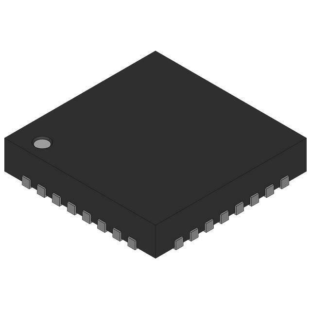


 工商网监
湘ICP备2023018690号
工商网监
湘ICP备2023018690号
