www.ti.com
Table of Contents
User’s Guide
UCC12050EVM-022 User's Guide
ABSTRACT
This user’s guide provides a description as well as directions for the use of UCC12050EVM-022 to evaluate
the UCC120xy family of isolated, high frequency, integrated transformer, DC/DC converter modules from Texas
Instruments. This EVM allows designers to quickly and efficiently evaluate the UCC120xy for use in electrically
isolated system designs. The EVM comes with UCC12050DVE populated by default but can accommodate any
of the pin-to-pin compatible, alternate versions listed in Table 1-1. The UCC12050DVE is the default descriptive
part number used throughout this document.
Table of Contents
1 Introduction.............................................................................................................................................................................2
2 Description.............................................................................................................................................................................. 3
3 Typical Application Circuit and Top Component View........................................................................................................4
4 Pin Configuration and Pin Functions....................................................................................................................................5
4.1 Pin Functions..................................................................................................................................................................... 5
5 EVM Setup and Operation......................................................................................................................................................6
5.1 U1 Component Selection................................................................................................................................................... 6
5.2 External Connections for Easy Evaluation......................................................................................................................... 6
5.3 High Voltage Isolation........................................................................................................................................................ 6
5.4 Enabling and Disabling the UCC12050..............................................................................................................................6
5.5 SYNC and SYNC_OK Functionality...................................................................................................................................6
5.6 Output Voltage Selection....................................................................................................................................................6
5.7 Test Points: TP1, TP2 & TP3............................................................................................................................................. 7
5.8 Board Level EMI Mitigation Techniques............................................................................................................................. 8
6 List of Materials.......................................................................................................................................................................9
7 Schematic..............................................................................................................................................................................10
8 Layout Diagrams................................................................................................................................................................... 11
9 Revision History................................................................................................................................................................... 14
List of Figures
Figure 3-1. Typical application circuit...........................................................................................................................................4
Figure 3-2. Top view of UCC12050EVM-022 Rev. A................................................................................................................... 4
Figure 5-1. Using the Pig Tail Test Points: TP1, TP2, TP3.......................................................................................................... 7
Figure 5-2. Comparison Between Voltage Measured by a Alligator Clip (Left) Versus Ground Spring (Right)........................... 8
Figure 8-1. Top Layer Composite...............................................................................................................................................11
Figure 8-2. Signal Layer 1......................................................................................................................................................... 12
Figure 8-3. Signal Layer 2......................................................................................................................................................... 13
Figure 8-4. Bottom Layer........................................................................................................................................................... 14
List of Tables
Table 1-1. UCC120xy IC Version Differences.............................................................................................................................. 2
Table 5-1. Output Voltage Regulation Selections........................................................................................................................ 7
Table 6-1. List of Materials...........................................................................................................................................................9
Trademarks
All trademarks are the property of their respective owners.
SLUUBD5D – SEPTEMBER 2019 – REVISED FEBRUARY 2022
Submit Document Feedback
Copyright © 2022 Texas Instruments Incorporated
UCC12050EVM-022 User's Guide
1
�Introduction
www.ti.com
1 Introduction
The UCC12050DVE is a high efficiency, low-emissions, 5 kVrms Isolated DC/DC Converter Module capable of
delivering up to 500 mW of power to isolated applications. Since the UCC12050DVE provides isolated power in
an integrated package, this allows systems to reduce cost and size by removing the need for separate isolated
power supplies. The UCC12050DVE delivers class-leading efficiency in power conversion from the primary to
the secondary side while removing the need for bulky external transformer or power modules common in current
designs. This integration allows for a much smaller area as well as a much shorter profile when compared to
industry standards for power isolation techniques used in the field today. The UCC12050DVE is the default IC
used in this EVM but any of the versions listed in Table 1-1 can be used for evaluation. Each of the component
versions listed in Table 1-1 are pin-to-pin compatible, functionally equivalent, drop in replacements with respect
to one another.
Table 1-1. UCC120xy IC Version Differences
2
Part Number
Isolation/Surge/Working Voltage
Automotive Qualification
UCC12040DVE
3 kVRMS/6.5 kVPK/850 VRMS
No
UCC12050DVE
5 kVRMS/10 kVPK/1.2 kVRMS
No
UCC12041QDVERQ1
3 kVRMS/6.5 kVPK/850 VRMS
Yes, AEC-Q100
UCC12051QDVERQ1
5 kVRMS/10 kVPK/1.2 kVRMS
Yes, AEC-Q100
UCC12050EVM-022 User's Guide
SLUUBD5D – SEPTEMBER 2019 – REVISED FEBRUARY 2022
Submit Document Feedback
Copyright © 2022 Texas Instruments Incorporated
�www.ti.com
Description
2 Description
The UCC12050EVM-022 is intended to allow designers to evaluate the performance characteristics and abilities
of the UCC12050DVE quickly and easily for use in isolated systems. The EVM allows users to test functions of
the UCC12050DVE such as: Enable/Disable the device easily, Sync the device with an external clock source,
detect potential external clock faults, select 5 V or 5.4 V output modes, and easily apply variable resistive loads
to the output.
This EVM allows the user to easily measure efficiency across the input voltage range and varying output loads
that the system might require. Section 5 documents how to make connections and measurements for testing
efficiency across varying loads. Another feature of this EVM is the test points, which are labeled as TP1,
TP2 and TP3, specially intended for use with oscilloscope probe ground springs, also known as pig tails, for
measuring small signals such as input/output ripple voltages.
SLUUBD5D – SEPTEMBER 2019 – REVISED FEBRUARY 2022
Submit Document Feedback
Copyright © 2022 Texas Instruments Incorporated
UCC12050EVM-022 User's Guide
3
�Typical Application Circuit and Top Component View
www.ti.com
3 Typical Application Circuit and Top Component View
Figure 3-1 shows the typical application circuit for UCC12050DVE.
10µF
10µF
RPU
0.1µF
1
EN
GNDS
16
2
GNDP
GNDS
15
3
VINP
VISO
14
4
SYNC
SEL
13
SYNC_OK
NC
12
6
NC
NC
11
7
NC
NC
10
8
NC
GNDS
5
RSYNC
UCC12050
0.1µF
Load
RSEL
9
Figure 3-1. Typical application circuit
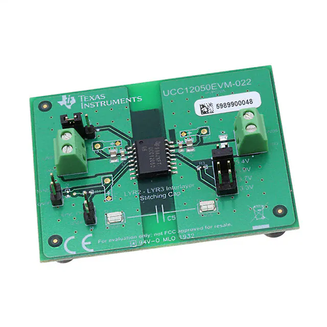
Figure 3-2 shows a top view picture of the EVM.
Figure 3-2. Top view of UCC12050EVM-022 Rev. A
4
UCC12050EVM-022 User's Guide
SLUUBD5D – SEPTEMBER 2019 – REVISED FEBRUARY 2022
Submit Document Feedback
Copyright © 2022 Texas Instruments Incorporated
�www.ti.com
Pin Configuration and Pin Functions
4 Pin Configuration and Pin Functions
EN
1
16
GNDS
GNDP
2
15
GNDS
VINP
3
14
VISO
SYNC
4
13
SEL
SYNC_OK
5
12
NC
NC
6
11
NC
NC
7
10
NC
NC
8
9
GNDS
DVE Package 16-Pin SOIC Top View
4.1 Pin Functions
PIN
NAME
NO.
I/O(1)
DESCRIPTION
EN
1
I
Active-high enable input. Connect EN to GNDP to disable the device. Connect EN to VINP to enable
the device. EN should be in the desired state (enabled/disabled) prior to power up.
GNDP
2
P
Ground return for primary side supply (VINP).
VINP
3
P
Primary side input supply voltage input. Connect a 10-μF ceramic capacitor between VINP and
GNDP, close to the device pins, for proper operation. Connect a 0.1µF ceramic capacitor in parallel
with the 10µF for additional high frequency filtering.
SYNC
4
I
Synchronous clock input pin. Provide a clock signal to synchronize multiple UCC12050 devices or
connect to GNDP for standalone operation using the internal oscillator. If the SYNC pin is left open it
should be separated from any switching noise to avoid false clock coupling.
5
O
Active-low, open-drain diagnostic output. Pin is asserted LOW if no external SYNC clock or one
that is outside of the operating range of the UCC12050 is detected. In this state, the external clock
is ignored and the DC/DC converter is clocked by the device's internal oscillator. The pin is in
high-impedance if a good clock is applied on SYNC.
SYNC_OK
NC
6, 7, 8
—
No internal connection. Connect NC to GNDP on printed circuit board.
GNDS
9, 15, 16
P
Ground return for secondary side (VISO).
NC
10, 11, 12
—
No internal connection. Connect NC to GNDS on printed circuit board.
SEL
13
I
VISO regulation voltage selection input. VISO regulation is selectable between 3.3V, 3.7V, 5.0V, and
5.4V using the SEL input. See for more details using SEL to select the VISO regulation threshold.
VISO
14
P
Isolated supply voltage output. Connect a 10-μF ceramic capacitor between VISO and GNDS, close
to the device pins, for proper operation. Connect a 0.1µF ceramic capacitor in parallel with the 10µF
for additional high frequency filtering.
(1)
P = Power, G = Ground, I = Input, O = Output
SLUUBD5D – SEPTEMBER 2019 – REVISED FEBRUARY 2022
Submit Document Feedback
Copyright © 2022 Texas Instruments Incorporated
UCC12050EVM-022 User's Guide
5
�EVM Setup and Operation
www.ti.com
5 EVM Setup and Operation
5.1 U1 Component Selection
This EVM comes with UCC12050DVE installed in the U1 reference designator position. Any of the alternate
versions listed in Table 1-1 can be exchanged in place of UCC12050DVE. If U1 replacement is required, it
is recommended to always use best practice soldering techniques. This can include taking appropriate ESD
precautions and having qualified personnel, skilled at surface mount soldering and board level rework, removing
and installing U1. Visually verify the desired UCC120xy component version is properly installed in the EVM. If
rework on U1 has previously been performed, visually verify correct orientation of U1 according to Figure 3-2.
The pin 1 locating dot on top of the IC package should be oriented at the top left according to Figure 3-2.
5.2 External Connections for Easy Evaluation
The UCC12050EVM-022 EVM utilizes screw terminals for quickly connecting to VINP and VISO. Connect a +5
V supply (+4.5 V to +5.5 V) between VINP and GNDP of J1 to supply power to the board. Connect a variable
load between VISO and GNDS of J6. Alternatively, R4 is available to solder down a load resistor directly to the
board. It is recommended to use an 0805 resistor that is rated for 0.5 W or greater. The value depends on the
application needs, but the load should not exceed 0.5 W.
5.3 High Voltage Isolation
The UCC12050DVE is capable of supporting reinforced isolation. To this end, the PCB in the UCC12050DVE is
designed to demonstrate proper layout techniques to enable reinforced isolation. The channel distance between
the primary and secondary side (including the GNDP to GNDS planes and VINP to VISO distance) satisfies
requirements for minimum required creepage and clearance distances to maintain reinforced isolation barrier
between the input side to the output side.
Note
This EVM is not intended for high voltage isolation testing, but merely to demonstrate proper isolation
board design.
5.4 Enabling and Disabling the UCC12050
The enable/disable function is easily evaluated using the jumper, J2. Connect the shunt between EN and VINP
to enable the UCC12050. Connect the shunt between EN and GNDP to disable the UCC12050 and place it in a
low-power state.
5.5 SYNC and SYNC_OK Functionality
J3 is provided to connect an external clock to the UCC12050. In order to synchronize multiple UCC12050
devices to a single clock source, connect an external oscillator (a function generator) between SYNC and GNDP.
The oscillator must be a 0 V to 5 V square wave at a frequency of double the desired switching frequency with a
50% duty cycle. The frequency must be within the specified operating range of the device, 14.4 MHz - 17.6 MHz.
The SYNC_OK output, J4, indicates when a valid clock source is connected to SYNC_OK. SYNC_OK is
high impedance when a valid clock is connected, and pulled to GNDP when no clock, or an invalid clock, is
connected to SYNC. SNYC_OK is pulled up to VINP on the EVM. R2 pads are available to place a termination
resistor on SYNC, if needed.
5.6 Output Voltage Selection
The SEL input determines the output voltage regulation threshold of VISO. The UCC12050EVM-022 provides
J5 to easily select between the different output voltage selections. J5 is clearly labeled to easily identify the
jumper position required for the desired output voltage. For reference, the SEL connection required to achieve a
particular ISO regulation is provided in Table 5-1. The device interprets the SEL pin as part of the startup routine,
so the SEL state at startup is used to set the regulation point. Any change to J5 has no effect during operation.
To change the output voltage regulation, it is required to disable the device (or power down), change the shunt to
the desired position, then enable (or power on) the UCC12050.
6
UCC12050EVM-022 User's Guide
SLUUBD5D – SEPTEMBER 2019 – REVISED FEBRUARY 2022
Submit Document Feedback
Copyright © 2022 Texas Instruments Incorporated
�www.ti.com
EVM Setup and Operation
Table 5-1. Output Voltage Regulation Selections
SEL Position
Output Voltage
SEL connected directly to VISO
5.0 V
SEL connected to VISO through 100 kΩ
5.4 V
SEL connected to GNDS through 100 kΩ
3.7 V
SEL connected directly to GNDS
3.3 V
5.7 Test Points: TP1, TP2 & TP3
Test points for VINP, VISO, and SYNC are provided on the EVM.
To get the cleanest measurement of output ripple using an oscilloscope, use probe tip with a ground spring.
This reduces the added noise that is introduced when using the longer alligator clip style ground lead. Figure 5-1
shows a picture illustrating how these test points are best used.
Comparison scope shots between the two grounding methods are shown in Figure 5-2.
Figure 5-1. Using the Pig Tail Test Points: TP1, TP2, TP3
SLUUBD5D – SEPTEMBER 2019 – REVISED FEBRUARY 2022
Submit Document Feedback
Copyright © 2022 Texas Instruments Incorporated
UCC12050EVM-022 User's Guide
7
�EVM Setup and Operation
www.ti.com
Figure 5-2. Comparison Between Voltage Measured by a Alligator Clip (Left) Versus Ground Spring
(Right)
5.8 Board Level EMI Mitigation Techniques
The UCC12050EVM-022 board layout is optimized for EMI performance. One EMI mitigation technique
demonstrated is an interlayer stitching capacitor (shown as C5 in the schematic). The GNDP and GNDS planes
on the inner layers (layer 2 and layer 3) are overlapped in order to form a common-mode, capacitive filter
between the two ground planes. GNDP on layer 2 and GNDS on layer 3 overlap. Note that the GND planes
do not go all the way to the edge of the board where they overlap. This is to illustrate how to satisfy isolation
requirements. There is sufficient distance between the edge of the overlapping layers using this methodology.
This only must be used when the planes overlap close to the edge of the board. The second EMI mitigation
technique used is the use of stitch vias in the GND planes (GNDP and GNDS) to further suppress EM
transmissions.
8
UCC12050EVM-022 User's Guide
SLUUBD5D – SEPTEMBER 2019 – REVISED FEBRUARY 2022
Submit Document Feedback
Copyright © 2022 Texas Instruments Incorporated
�www.ti.com
List of Materials
6 List of Materials
Table 6-1. List of Materials
Designator
Qty
Description
Part Number
Manufacturer
C1, C4
2
Capacitor, ceramic, 10 uF, 16 V, +/- 10%, X7R, 0805
CL21B106KOQNNNE
Samsung Electro-Mechanics
(C1, C4)-alternate
0
Capacitor, ceramic, 10 uF, 16 V, +/- 10%, X7S, 0805, AEC-Q200
CL21Y106KOQ4PNE
Samsung Electro-Mechanics
C2, C3
2
Capacitor, ceramic, 0.1 µF, 50 V,+/- 10%, X7R, AEC-Q200 Grade 1,
0603
06035C104KAZ2A
AVX
J1, J6
2
Conn term block, 2POS, 3.81mm, TH
1727010
Phoenix Contact
J2
1
Header, 100 mil, 3x1, Tin, TH
PEC03SAAN
Sullins Connector Solutions
J3, J4, J5
3
Header, 100 mil, 2x1, Tin, TH
PEC02SAAN
Sullins Connector Solutions
R1, R3
2
Resistor, 100 kΩ, 5%, 0.063 W, AEC-Q200 Grade 0, 0402
CRCW0402100KJNED
Vishay-Dale
R2
0
Termination resistor for SYNC, 0402, DNP
R4
0
Load resistor, 0805, DNP
TP4, TP5
2
Test point, Miniature, SMT
5019
Keystone
U1
1
500 mW, High-Efficiency, Low-Emissions, 5 kVRMS Isolated DC/DC
Converter, DVE0016A (SO-MOD-16)
UCC12050DVE
Texas Instruments
U1-alternate
0
500 mW, High-Efficiency, Low-Emissions, 3 kVRMS Isolated DC/DC
Converter, DVE0016A (SO-MOD-16)
UCC12040DVE
Texas Instruments
U1-alternate
0
500 mW, High-Efficiency, Low-Emissions, 3 kVRMS Isolated DC/DC
Converter AEC-Q100, DVE0016A (SO-MOD-16)
UCC12041QDVERQ1
Texas Instruments
U1-alternate
0
500 mW, High-Efficiency, Low-Emissions, 5 kVRMS Isolated DC/DC
Converter AEC-Q100, DVE0016A (SO-MOD-16)
UCC12051QDVERQ1
Texas Instruments
FID1, FID2, FID3
0
Fiducial mark. There is nothing to buy or mount.
N/A
N/A
SLUUBD5D – SEPTEMBER 2019 – REVISED FEBRUARY 2022
Submit Document Feedback
UCC12050EVM-022 User's Guide
Copyright © 2022 Texas Instruments Incorporated
9
�List of Materials
www.ti.com
7 Schematic
10
UCC12050EVM-022 User's Guide
SLUUBD5D – SEPTEMBER 2019 – REVISED FEBRUARY 2022
Submit Document Feedback
Copyright © 2022 Texas Instruments Incorporated
�www.ti.com
Layout Diagrams
8 Layout Diagrams
Figure 8-1. Top Layer Composite
SLUUBD5D – SEPTEMBER 2019 – REVISED FEBRUARY 2022
Submit Document Feedback
Copyright © 2022 Texas Instruments Incorporated
UCC12050EVM-022 User's Guide
11
�Layout Diagrams
www.ti.com
Figure 8-2. Signal Layer 1
12
UCC12050EVM-022 User's Guide
SLUUBD5D – SEPTEMBER 2019 – REVISED FEBRUARY 2022
Submit Document Feedback
Copyright © 2022 Texas Instruments Incorporated
�www.ti.com
Layout Diagrams
Figure 8-3. Signal Layer 2
SLUUBD5D – SEPTEMBER 2019 – REVISED FEBRUARY 2022
Submit Document Feedback
Copyright © 2022 Texas Instruments Incorporated
UCC12050EVM-022 User's Guide
13
�Revision History
www.ti.com
Figure 8-4. Bottom Layer
9 Revision History
NOTE: Page numbers for previous revisions may differ from page numbers in the current version.
Changes from Revision C (June 2021) to Revision D (February 2022)
Page
• Updated EN description......................................................................................................................................5
Changes from Revision B (January 2021) to Revision C (June 2021)
Page
• Added UCC12041QDVERQ1 to Table 1-1 ........................................................................................................ 2
• Changed UCC12051DVE-Q1 to UCC12051QDVERQ1 in Table 1-1 ................................................................ 2
• Updated the surge voltage for UCC12040DVE in Table 1-1 ..............................................................................2
• Added UCC12041QDVERQ1 to Table 6-1 ........................................................................................................ 9
• Changed UCC12051DVE-Q1 to UCC12051QDVERQ1 in Table 6-1 ................................................................ 9
Changes from Revision Original (January 2021) to Revision B (January 2021)
Page
• Updated device links...........................................................................................................................................1
Changes from Revision Original (September 2019) to Revision A (January 2021)
Page
• Added details to support UCC12040 and the UCC12051-Q1............................................................................ 1
14
UCC12050EVM-022 User's Guide
SLUUBD5D – SEPTEMBER 2019 – REVISED FEBRUARY 2022
Submit Document Feedback
Copyright © 2022 Texas Instruments Incorporated
�IMPORTANT NOTICE AND DISCLAIMER
TI PROVIDES TECHNICAL AND RELIABILITY DATA (INCLUDING DATA SHEETS), DESIGN RESOURCES (INCLUDING REFERENCE
DESIGNS), APPLICATION OR OTHER DESIGN ADVICE, WEB TOOLS, SAFETY INFORMATION, AND OTHER RESOURCES “AS IS”
AND WITH ALL FAULTS, AND DISCLAIMS ALL WARRANTIES, EXPRESS AND IMPLIED, INCLUDING WITHOUT LIMITATION ANY
IMPLIED WARRANTIES OF MERCHANTABILITY, FITNESS FOR A PARTICULAR PURPOSE OR NON-INFRINGEMENT OF THIRD
PARTY INTELLECTUAL PROPERTY RIGHTS.
These resources are intended for skilled developers designing with TI products. You are solely responsible for (1) selecting the appropriate
TI products for your application, (2) designing, validating and testing your application, and (3) ensuring your application meets applicable
standards, and any other safety, security, regulatory or other requirements.
These resources are subject to change without notice. TI grants you permission to use these resources only for development of an
application that uses the TI products described in the resource. Other reproduction and display of these resources is prohibited. No license
is granted to any other TI intellectual property right or to any third party intellectual property right. TI disclaims responsibility for, and you
will fully indemnify TI and its representatives against, any claims, damages, costs, losses, and liabilities arising out of your use of these
resources.
TI’s products are provided subject to TI’s Terms of Sale or other applicable terms available either on ti.com or provided in conjunction with
such TI products. TI’s provision of these resources does not expand or otherwise alter TI’s applicable warranties or warranty disclaimers for
TI products.
TI objects to and rejects any additional or different terms you may have proposed. IMPORTANT NOTICE
Mailing Address: Texas Instruments, Post Office Box 655303, Dallas, Texas 75265
Copyright © 2022, Texas Instruments Incorporated
�


 工商网监
湘ICP备2023018690号
工商网监
湘ICP备2023018690号
