2N2102
2N2102A
SILICON
NPN TRANSISTOR
w w w. c e n t r a l s e m i . c o m
DESCRIPTION:
The CENTRAL SEMICONDUCTOR 2N2102,A is a
silicon NPN epitaxial planar transistor designed for high
current general purpose switching applications.
MARKING: FULL PART NUMBER
TO-39 CASE
MAXIMUM RATINGS: (TA=25°C unless otherwise noted)
SYMBOL UNITS
Collector-Base Voltage
VCBO 120 V
Collector-Emitter Voltage
VCER 80 V
Collector-Emitter Voltage
VCEO 65
V
Emitter-Base Voltage
VEBO 7.0
V
Continuous Collector Current
IC 1.0 A
Power Dissipation (TC=25°C) PD 5.0 W
Power Dissipation
PD 1.0 W
Operating and Storage Junction Temperature
Thermal Resistance
Thermal Resistance
TJ, Tstg
-65 to +200
°C
ΘJA 175 °C/W
ΘJC 35 °C/W
ELECTRICAL CHARACTERISTICS: (TA=25°C unless otherwise noted)
SYMBOL
TEST CONDITIONS
MIN
MAX
UNITS
ICBO VCB=60V 2.0
nA
ICBO VCB=60V, TA=150°C
2.0
μA
IEBO VEB=5.0V 2.0
nA
BVCBO IC=100µA
120 V
BVCER IC=100mA, RBE=10Ω 80 V
BVCEO IC=100mA
65 V
BVEBO IE=100µA
7.0 V
VCE(SAT) IC=150mA, IB=15mA (2N2102)
0.5
V
VCE(SAT) IC=150mA, IB=15mA (2N2102A)
0.3
V
VBE(SAT) IC=150mA, IB=15mA 1.1 V
hFE VCE=10V, IC=10μA 10
hFE VCE=10V, IC=100μA 20
hFE VCE=10V, IC=10mA 35
hFE VCE=10V, IC=10mA, TA=-55°C 20
hFE VCE=10V, IC=150mA 40 200
hFE VCE=10V, IC=500mA 25
R0 (19-October 2022)
�2N2102
2N2102A
SILICON
NPN TRANSISTOR
ELECTRICAL CHARACTERISTICS - Continued: (TA=25°C unless otherwise noted)
SYMBOL
TEST CONDITIONS
MIN
MAX
UNITS
hFE VCE=10V, IC=1.0A 10
hfe VCE=5.0V, IC=1.0mA, f=1.0kHz
30
100
hfe VCE=10V, IC=5.0mA, f=1.0kHz
35
hib VCE=5.0V, IC=1.0mA, f=1.0kHz
24
34
Ω
hib VCE=10V, IC=5.0mA, f=1.0kHz
4.0
hrb VCE=5.0V, IC=1.0mA, f=1.0kHz
8.0
Ω
3x10⁻⁴
hrb VCE=10V, IC=5.0mA, f=1.0kHz
hob VCE=5.0V, IC=1.0mA, f=1.0kHz
0.08
0.5
hob VCE=10V,
fT VCE=10V,
IC=5.0mA, f=1.0kHz
IC=50mA, f=20MHz
0.08
150
3x10⁻⁴
1.0
60
μS
μS
MHz
Cob VCB=10V, IE=0, f=100kHz
15
Cib VEB=0.5V, IC=0, f=100kHz
80
pF
pF
NF VCE=10V, IC=300μA, f=1.0kHz
6.0
dB
R0 (19-October 2022)
w w w. c e n t r a l s e m i . c o m
�2N2102
2N2102A
SILICON
NPN TRANSISTOR
TO-39 CASE - MECHANICAL OUTLINE
LEAD CODE:
1) Emitter
2) Base
3) Collector
MARKING: FULL PART NUMBER
R0 (19-October 2022)
w w w. c e n t r a l s e m i . c o m
�OUTSTANDING SUPPORT AND SUPERIOR SERVICES
PRODUCT SUPPORT
Central’s operations team provides the highest level of support to insure product is delivered on-time.
• Supply management (Customer portals)
• Custom bar coding for shipments
• Inventory bonding
• Custom product packing
• Consolidated shipping options
DESIGNER SUPPORT/SERVICES
Central’s applications engineering team is ready to discuss your design challenges. Just ask.
• Free quick ship samples (2nd day air)
• Special wafer diffusions
• Online technical data and parametric search
• PbSn plating options
• SPICE models
• Package details
• Custom electrical curves
• Application notes
• Environmental regulation compliance
• Application and design sample kits
• Customer specific screening
• Custom product and package development
• Up-screening capabilities
REQUESTING PRODUCT PLATING
1. If requesting Tin/Lead plated devices, add the suffix “ TIN/LEAD” to the part number when
ordering (example: 2N2222A TIN/LEAD).
2. If requesting Lead (Pb) Free plated devices, add the suffix “ PBFREE” to the part number
when ordering (example: 2N2222A PBFREE).
CONTACT US
Corporate Headquarters & Customer Support Team
Central Semiconductor Corp.
145 Adams Avenue
Hauppauge, NY 11788 USA
Main Tel: (631) 435-1110
Main Fax: (631) 435-1824
Support Team Fax: (631) 435-3388
www.centralsemi.com
Worldwide Field Representatives:
www.centralsemi.com/wwreps
Worldwide Distributors:
www.centralsemi.com/wwdistributors
For the latest version of Central Semiconductor’s LIMITATIONS AND DAMAGES DISCLAIMER,
which is part of Central’s Standard Terms and Conditions of sale, visit: www.centralsemi.com/terms
w w w. c e n t r a l s e m i . c o m
(001)
�
很抱歉,暂时无法提供与“2N2102”相匹配的价格&库存,您可以联系我们找货
免费人工找货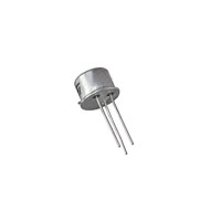


 工商网监
湘ICP备2023018690号
工商网监
湘ICP备2023018690号
