CS61581
T1/E1 Universal Line Interface
Features
– FCC Rules and Regulations: Part 68 and Part
15
– AT&T Publication 62411
– ETSI ETS 300 011, 300 233, TBR 12/13
– TR-NET-00499
l Provides
T1 and E1, Long Haul and Short
Haul Line Interface
l Provides a QRSS Test Signal and Error
Detector
l Impedance Matching Line Driver Using a
Single Transformer
l Greater than 14 dB of Transmit Return Loss
Without Using External Resistors
l No Crystal Needed for Jitter Attenuation
l Meets AT&T 62411 and TBR 12/13 Jitter
Tolerance and Attenuation Requirements
l Meets ANSI T1.231B and ITU-T G.775
Requirements for LOS and AIS
l Meets the BS6450 Transmitter Short-Circuit
Requirements for E1 Applications
l Compliant with:
Description
The CS61581 is a primary rate line interface unit capable of operation in both short haul (intraoffice) and long
haul applications. The CS61581 combines the complete analog transmit and receive circuitry for a single,
full-duplex interface at T1 and E1 rates. The device is
pin and function compatible with the Level One LXT310
and LXT318 (the latter in the host mode only). The device can also replace LXT359 and LXT360. Enhanced
functionality is available through an extended register
set allowing short haul operation, custom pulse shape
generation, QRSS pattern generation, detection and error counting, and generation and detection of loop up
and loop down codes. The CS61581 features Crystal®
low-power impedance-matched line drivers and crystalless jitter attenuation.
– ITU-T Recommendations: G.703, G.732,
G.775 and I.431
– American National Standards (ANSI): T1.102,
T1.105, T1.403, T1.408, and T1.231
TCLK
TDATA/TPOS
UBS/TNEG
JASEL
2
3
4
E
N
C
O
D
E
R
JITTER
ATTEN
ORDERING INFORMATION
CS61581-IL
28-pin PLCC
CS61581-IP
28-pin PDIP
PULSE
SHAPING
CIRCUITRY
ROM / RAM
TRANSMIT
TIMING &
CONTROL
Q
R
S
S
RDATA/RPOS
BPV/RNEG
16
28
26
27
24
11
TAOS Enable
RCLK
13
LINE DRIVERS
D
8 E
C
7 O
D
6
E
R
REMOTE
LOOPBACK
LOCAL
LOOPBACK
(DIGITAL)
SERIAL
PORT
25
REGISTERS & CONTROL LOGIC
LOS/
NLOOP
Clear
JITTER
ATTEN
LBO Select
SH/LH
TIMING
& DATA
RECOVERY
LLOOP
Enable
TRING
CLKE/TAOS
CS/RLOOP
SCLK/LLOOP
SDI/LBO1
SDO/LBO2
LOCAL
LOOPBACK
(ANALOG)
EQUALIZER
CONTROL
SLICERS
& PEAK
DETECT
TTIP
18
SH
NOISE &
CROSSTALK
FILTERS
MAGNITUDE
EQUALIZER
19
20
AGC
LATN
RTIP
RRING
SH
INT/NLOOP
LOS
23
12
INBAND
NLOOP
& LOS
PROCESSOR
RECEIVE
CLOCK
GENERATOR
9
XTALIN
Preliminary Product Information
P.O. Box 17847, Austin, Texas 78760
(512) 445 7222 FAX: (512) 445 7581
http://www.cirrus.com
10
XTALOUT
1
5
MODE
21
RV+
22
14
RGND TGND
MCLK
15
TV+
This document contains information for a new product.
Cirrus Logic reserves the right to modify this product without notice.
Copyright Cirrus Logic, Inc. 2000
(All Rights Reserved)
DS211PP8
APR ‘00
1
�CS61581
TABLE OF CONTENTS
1. CHARACTERISTICS AND SPECIFICATIONS ..................................................................4
ABSOLUTE MAXIMUM RATINGS .....................................................................4
RECOMMENDED OPERATING CONDITIONS .................................................4
DIGITAL CHARACTERISTICS...........................................................................4
ANALOG SPECIFICATIONS..............................................................................5
T1 SWITCHING CHARACTERISTICS ...............................................................7
E1 SWITCHING CHARACTERISTICS...............................................................7
SWITCHING CHARACTERISTICS ....................................................................9
2. THEORY OF OPERATION ...............................................................................................10
2.1 Operating Mode Selection ........................................................................10
2.2 Master Clocks ...........................................................................................10
2.3 Transmitter ................................................................................................10
2.4 Transmit All Ones Select ..........................................................................12
2.4.1 Receiver ..........................................................................................13
2.4.2 Short Haul .......................................................................................13
2.4.3 Long Haul ........................................................................................13
2.4.4 Clock Recovery ...............................................................................13
2.4.5 Jitter Tolerance ...............................................................................14
2.5 Receiver Line Attenuation Indication ........................................................14
2.6 Jitter Attenuator ........................................................................................14
2.7 Receiver Loss of Signal ............................................................................14
2.8 Local Loopback ........................................................................................15
2.9 Remote Loopback .....................................................................................16
2.10 Network Loopback ..................................................................................16
2.11 Alarm Indication Signal ...........................................................................16
2.12 Serial Interface .......................................................................................16
2.21 Interrupts ................................................................................................23
3. QRSS TEST MODE ..........................................................................................................23
4. ARBITRARY WAVEFORM GENERATION ......................................................................24
4.1 Power On Reset / Reset ...........................................................................25
4.2 Power Supply ............................................................................................26
6. PIN DESCRIPTION ...........................................................................................................31
6.1 Power Supplies .........................................................................................32
6.2 Oscillator ...................................................................................................32
6.3 Control ......................................................................................................32
6.4 Status .......................................................................................................33
6.5 Serial Control Interface .............................................................................33
6.6 Data Input/Output .....................................................................................34
7. PACKAGE DIMENSIONS ................................................................................................36
Contacting Cirrus Logic Support
For a complete listing of Direct Sales, Distributor, and Sales Representative contacts, visit the Cirrus Logic web site at:
http://www.cirrus.com/corporate/contacts/
Preliminary product information describes products which are in production, but for which full characterization data is not yet available. Advance product information describes products which are in development and subject to development changes. Cirrus Logic, Inc. has made best efforts to ensure that the information
contained in this document is accurate and reliable. However, the information is subject to change without notice and is provided “AS IS” without warranty of
any kind (express or implied). No responsibility is assumed by Cirrus Logic, Inc. for the use of this information, nor for infringements of patents or other rights
of third parties. This document is the property of Cirrus Logic, Inc. and implies no license under patents, copyrights, trademarks, or trade secrets. No part of
this publication may be copied, reproduced, stored in a retrieval system, or transmitted, in any form or by any means (electronic, mechanical, photographic, or
otherwise) without the prior written consent of Cirrus Logic, Inc. Items from any Cirrus Logic website or disk may be printed for use by the user. However, no
part of the printout or electronic files may be copied, reproduced, stored in a retrieval system, or transmitted, in any form or by any means (electronic, mechanical,
photographic, or otherwise) without the prior written consent of Cirrus Logic, Inc.Furthermore, no part of this publication may be used as a basis for manufacture
or sale of any items without the prior written consent of Cirrus Logic, Inc. The names of products of Cirrus Logic, Inc. or other vendors and suppliers appearing
in this document may be trademarks or service marks of their respective owners which may be registered in some jurisdictions. A list of Cirrus Logic, Inc. trademarks and service marks can be found at http://www.cirrus.com.
2
DS211PP8
�CS61581
LIST OF FIGURES
Figure 1. Signal Rise and Fall Characteristics ............................................................................... 8
Figure 2. Recovered Clock and Data Switching Characteristics.................................................... 8
Figure 3. Transmit Clock and Data Switching Characteristics ....................................................... 8
Figure 4. Serial Port Write Timing Diagram ................................................................................... 9
Figure 5. Serial Port Read Timing Diagram ................................................................................... 9
Figure 6. Typical Pulse Shape at DSX-1 Cross Connect............................................................. 12
Figure 7. Mask of the Pulse at the 2048 kbps Interface............................................................... 12
Figure 8. Minimum Input Jitter Tolerance of Receiver ................................................................. 13
Figure 9. LATN Pulse Width encoding ......................................................................................... 14
Figure 10.Typical Jitter Transfer Function - T1 ............................................................................. 15
Figure 11.Typical Jitter Transfer Function - E1 ............................................................................. 15
Figure 12.Input/Output Timing (showing address 0x10) ............................................................... 17
Figure 13.Phase Definition of Arbitrary Waveforms ...................................................................... 24
Figure 14.Example of Summing of Waveforms............................................................................. 25
Figure 15.Matched Impedance Output Configuration ................................................................... 28
Figure 16.Low Impedance Output Configuration .......................................................................... 29
Figure 17.Typical System Connection .......................................................................................... 30
LIST OF TABLES
Table 1. Pulse Shape Selection and Transformer Requirements ................................................. 11
Table 2. Data Output/Clock Relationship ...................................................................................... 13
Table 3. Register Map................................................................................................................... 17
Table 4. Register 0x10 Decoding.................................................................................................. 23
Table 5. Register 0x10 Decoding.................................................................................................. 23
Table 5. Diagnostic Mode Availability ........................................................................................... 26
Table 6. Transformer Specification ............................................................................................... 26
Table 7. Recommended Transformers for the CS61581 .............................................................. 27
DS211PP8
3
�CS61581
1. CHARACTERISTICS AND SPECIFICATIONS
ABSOLUTE MAXIMUM RATINGS
Parameter
Symbol
Min
Max
Units
RV+
TV+
-
6.0
(RV+) + 0.3
V
V
Vin
RGND-0.3
(RV+) + 0.3
V
Iin
-10
10
mA
Ambient Operating Temperature
TA
-40
85
°C
Storage Temperature
Tstg
-65
150
°C
DC Supply
(referenced to RGND=TGND=0 V)
Input Voltage, Any Pin
Input Current, Any Pin
(Note 1)
WARNING: Operations at or beyond these limits may result in permanent damage to the device.
Normal operation is not guaranteed at these extremes
Notes: 1 Transient currents of up to 100 mA will not cause SCR latch-up. Also TTIP, TRING, TV+ and TGND
can withstand a continuous current of 100 mA.
RECOMMENDED OPERATING CONDITIONS
Parameter
DC Supply
Ambient Operating Temperature
Power Consumption, Long Haul
Power Consumption, Short Haul
Symbol
(Note 1) RV+, TV+
TA
(Notes 2,3,4)
PC
Low Z
Match Z
(Notes 2,3,4)
PC
Low Z
Match Z
Min
Typ
Max
Units
4.75
-40
5.0
25
5.25
85
V
°C
-
390
400
630
575
mW
-
480
430
725
650
mW
Notes: 1. TV+ must not exceed RV+ by more than 0.3 V.
2. Power consumption while driving line load over operating temperature range. Includes IC and load.
Digital input levels are within 10% of the supply rails and digital outputs are driving a 50 pF capacitive
load.
3. Typical consumption corresponds to 50% ones density and medium line length at 5.0 V.
4. Maximum consumption corresponds to 100% ones density and maximum line length at 5.25 V.
DIGITAL CHARACTERISTICS (TA = -40°C to 85°C; TV+, RV+ = 5.0 V ±5%; GND = 0 V)
Parameter
High-Level Input Voltage
High-Level Output Voltage
IOUT = -40 µA
(Note 5)
PINS 1-4, 24-28
(Note 5)
PINS 1-4, 24-28
(Notes 5, 6)
PINS 6-8, 25
Low-Level Output Voltage
IOUT = 1.6 mA
(Notes 5, 6)
PINS 6-8, 25
Low-Level Input Voltage
Input Leakage Current
Symbol
Min
Typ
Max
Units
VIH
2.0
-
-
V
VIL
-
-
0.8
V
VOH
2.4
-
-
V
VOL
-
-
0.4
V
-
-
±10
µA
Notes: 5. This specification guarantees TTL compatibility (VOH = 2.4 V @ IOUT = -40 µA).
6. Output drivers are TTL compatible and will drive CMOS logic levels into a CMOS load.
4
DS211PP8
�CS61581
ANALOG SPECIFICATIONS (TA = -40°C to 85°C; TV+, RV+ = 5.0 V ±5%; GND = 0 V)
Parameter
Min
Typ
Max
Units
2.14
2.7
2.7
2.4
4.8
2.37
3.0
3.0
3.0
5.6
2.6
3.3
3.3
3.6
6.4
V
V
V
V
V
Transmitter
AMI Output Pulse Amplitudes
(Note 7)
E1, 75 Ω (Note 8)
E1, 120 Ω (Note 9)
T1, (FCC Part 68) (Note 10)
T1, DSX-1 (Note 11)
External Equalizer Pulse Amplitude
Transmitter Output Impedance
(Note 13)
Transformer turns ratio = 1:2
Low Z, Long Haul
Transformer turns ratio = 1:1.5
Jitter Added by the Transmitter
E1, 75 Ω
E1, 120 Ω
T1, FCC
T1, DSX1
T1, Ext. Equal
(Note 12, 13)
10 Hz - 8 kHz
8k Hz - 40 kHz
10 Hz - 40 kHz
Broad Band
(Notes 7, 18)
(Notes 7, 18)
Power in 2 kHz band about 772 kHz
Power in 2 kHz band about 1.544 MHz
(referenced to power in 2 kHz band at 772 kHz)
Positive to Negative Pulse Imbalance
(Notes 7, 13)
Transmitter Short Circuit Current
(Notes 7, 14)
Ω
Ω
Ω
Ω
Ω
Ω
1.5
33
53
44
44
44
12.6
-29
0.015
0.015
0.015
0.020
15
-38
17.9
-
UI
UI
UI
UI
dBm
dB
-
0.2
-
0.5
50
dB
mA RMS
Notes: 7. Using a 0.47 µF capacitor in series with the primary of a transformer recommended in the Applications
Section.
8. Pulse amplitude measured at the output of the transformer across a 75 Ω load for line length settings
LEN[2:0] = 001 and 000.
9. Pulse amplitude measured at the output of the transformer across a 120 Ω load for line length setting
LEN[2:0] = 000.
10. Pulse amplitude measured at the output of the transformer across a 100 Ω load for line length setting
LEN[2:0] = 000.
11. Pulse amplitude measured at the DSX-1 Cross-Connect for all line length settings from LEN[2:0] = 011
to LEN[2:0] = 111.
12. Assuming that jitter free clock is input to TCLK. Jitter Attenuator not in path.
13. Not production tested. Parameters guaranteed by design and characterization.
14. Measured broadband through a 0.5 Ω resistor across the secondary of the transmitter transformer
during the transmission of an all ones data pattern with LEN[2:0] = 000 or 001.
DS211PP8
5
�CS61581
ANALOG SPECIFICATIONS (Continued)
Parameter
Receiver
RTIP/RRING Input Impedance
Sensitivity Below DSX (0 dB = 3.0 V) Long Haul, T1
Sensitivity Below DSX (0 dB = 3.0 V) Long Haul, E1
Sensitivity Below DSX (0 dB = 3.0 V) T1 - Short Haul
Sensitivity Below G.703 (0 dB = 2.4 V) E1 - Short Haul
Loss of Signal Threshold (Note 18)
Min
Typ
Max
Units
-40
30
-36
48
-21
270
-15
430
-
20k
-42
-22
-16
-
Ω
dB
mV
dB
mV
dB
mV
dB
mV
dB
dB
dB
Long Haul, T1 & E1
T1 Short Haul
E1 Short Haul
Data Decision Threshold (Note 18)
(Note 15)
T1, DSX-1
T1, (FCC Part 68) and E1
Allowable Consecutive Zeros before LOS
Receiver Input Jitter Tolerance - Short Haul
(Note 16)
E1: 18 kHz - 100 kHz
T1: 10 kHz - 100 kHz
(Note 13) 2 kHz
(Note 18) 10 Hz and below
160
50
50
175
190
% of peak
% of peak
bits
0.20
0.4
6.0
300
-
-
UI
UI
UI
UI
Receiver Input Jitter Tolerance - Long Haul
(Note 17)
E1:10 kHz - 100 kHz
T1:10 kHz - 100 kHz
(Note 13) 1 Hz
0.20
0.4
138
-
-
UI
UI
UI
Notes: 15. Data decision threshold established after the receiver equalizer filters pulse overshoot and undershoot.
16. Jitter tolerance for 0 dB input signal level. Jitter tolerance increases at lower frequencies. See Figure 8.
17. See Receiver Jitter Tolerance Plot, Figure 8.
18. Guaranteed by design.
6
DS211PP8
�CS61581
T1 SWITCHING CHARACTERISTICS (TA = -40°C to 85°C; TV+, RV+ = 5.0 V ±5%;
GND = 0 V; Inputs: Logic 0 = 0 V, Logic 1 = RV+; See Figures 1, 2, & 3)
Parameter
TCLK Frequency
MCLK Frequency
(Note 19)
Symbol
Min
Typ
Max
Units
ftclk
-
1.544
-
MHz
fmclk
-
1.544
-
MHz
(Notes 18, 20) tpwh1/tpw1
RCLK Duty Cycle
50
%
Rise Time, All Digital Outputs
(Note 21)
tr
-
-
85
ns
Fall Time, All Digital Outputs
(Note 21)
tf
-
-
85
ns
TPOS/TNEG to TCLK Falling Setup Time
tsu2
25
-
-
ns
TCLK Falling to TPOS/TNEG Hold Time
th2
25
-
-
ns
RPOS/RNEG Valid Before RCLK Falling
(Note 22)
tsu1
150
274
-
ns
RPOS/RNEG Valid Before RCLK Rising
(Note 23)
tsu1
150
274
-
ns
RPOS/RNEG Valid After RCLK Falling
(Note 22)
th1
150
274
-
ns
RPOS/RNEG Valid After RCLK Rising
(Note 23)
th1
150
274
-
ns
Notes: 19. MCLK provided by an external source or TCLK.
20. RCLK duty cycle will be 62.5% or 37.5% when jitter attenuator FIFO limits are reached.
21. At max load of 1.6 mA and 50 pF.
22. Host Mode (CLKE = 1).
23. Host Mode (CLKE = 0)
E1 SWITCHING CHARACTERISTICS (TA = -40°C to 85°C; TV+, RV+ = 5.0 V ±5%;
GND = 0 V; Inputs: Logic 0 = 0 V, Logic 1 = RV+; See Figures 1, 2, & 3)
Parameter
TCLK Frequency
MCLK Frequency
RCLK Duty Cycle
(Note 19)
Symbol
Min
Typ
Max
Units
ftclk
-
2.048
-
MHz
fmclk
-
2.048
-
MHz
(Notes 18, 20) tpwh1/tpw1
50
%
Rise Time, All Digital Outputs
(Note 21)
tr
-
-
85
ns
Fall Time, All Digital Outputs
(Note 21)
tf
-
-
85
ns
TPOS/TNEG to TCLK Falling Setup Time
tsu2
25
-
-
ns
TCLK Falling to TPOS/TNEG Hold Time
th2
25
-
-
ns
RPOS/RNEG Valid Before RCLK Falling
(Note 22)
tsu1
100
194
-
ns
RPOS/RNEG Valid Before RCLK Rising
(Note 23)
tsu1
100
194
-
ns
RPOS/RNEG Valid After RCLK Falling
(Note 22)
th1
100
194
-
ns
RPOS/RNEG Valid After RCLK Rising
(Note 23)
th1
100
194
-
ns
DS211PP8
7
�CS61581
tr
Any Digital Output
tf
90%
10%
90%
10%
Figure 1. Signal Rise and Fall Characteristics
tpw1
RCLK
(CLKE = 1)
t pwl1
RPOS
RNEG
t pwh1
t su1
t h1
(CLKE = 0)
RCLK
Figure 2. Recovered Clock and Data Switching Characteristics
t pw2
t pwh2
TCLK
t su2
t h2
TPOS/TNEG
Figure 3. Transmit Clock and Data Switching Characteristics
8
DS211PP8
�CS61581
SWITCHING CHARACTERISTICS (TA = -40° to 85°C; TV+, RV+ = 5V ±5%;
Inputs: Logic 0 = 0 V, Logic 1 = RV+)
Parameter
Symbol
Min
Typ
Max
Units
SDI to SCLK Setup Time
tdc
50
-
-
ns
SCLK to SDI Hold Time
tcdh
50
-
-
ns
SCLK Low Time
tcl
240
-
-
ns
SCLK High Time
tch
240
-
-
ns
SCLK Rise and Fall Time
tr, tf
-
-
50
ns
CS to SCLK Setup Time
tcc
50
-
-
ns
SCLK to CS Hold Time
tcch
50
-
-
ns
CS Inactive Time
tcwh
250
-
-
ns
tcdv
-
-
200
ns
tcdz
-
100
-
ns
SCLK to SDO Valid
(Note 24)
CS to SDO High Z
Notes: 24. Output load capacitance = 50 pF
t cwh
CS
t cc
t cch
t ch
t cl
SCLK
t cdh
t dc
SDI
t cdh
LSB
LSB
CONTROL
BYTE
MSB
DATA
BYTE
Figure 4. Serial Port Write Timing Diagram
CS
SCLK
SDI
LAST ADDR BIT
t cdv
SDO
CLKE = 0
t cdz
D0
D1
D6
D7
t cdv
HIGH Z
SDO
CLKE = 1
D0
D1
D6
D7
Figure 5. Serial Port Read Timing Diagram
DS211PP8
9
�CS61581
2. THEORY OF OPERATION
The CS61581 Universal Line Interface supports T1
and E1 data rates for both short haul and long haul
applications. The transmitter complies with all
standard T1 and E1 applications without changing
transformers. Transmitter power consumption is
minimized using the impedance matching feature,
which eliminates external resistors for standard line
impedances. When configured for long haul operation, the receiver uses gain and equalization to provide 40 dB of sensitivity. The receiver reconfigures
for short haul operation, limiting the receive sensitivity and increasing the noise immunity.
2.1
Operating Mode Selection
The CS61581 can be operated in stand-alone hardware interface mode (MODE pin is low), or by a
microcontroller in serial host mode (MODE pin is
high). Additional functionality is available in the
host mode including both short haul and long haul
operational modes. The CS61581 defaults to the
Long Haul configuration (LXT310/318 compatible). The T1 (DSX-1 and Network interface) and
E1 (ITU-T G.703) are selectable via the serial port
by writing to a control register.
Tying TNEG high for more than 16 TCLK cycles
enables the unipolar mode, changing TPOS to
TDATA, RPOS to RDATA, and RNEG to BPV.
When configured for unipolar mode, the MODE
pin can be tied to RCLK enabling the B8ZS encoders and decoders. Coder mode does not support bipolar data.
2.2
Master Clocks
The CS61581 requires a reference clock for the receiver and the jitter attenuator. Either a 1.544 MHz
(or 2.048 MHz) external clock can be input to
MCLK, or a 4X crystal can be connected to the onchip oscillator. This frequency reference should be
within 100 ppm of the nominal operating frequency. Jitter and wander on the reference clock will degrade jitter attenuation and receiver jitter tolerance.
10
If MCLK is provided, the crystal oscillator is ignored.
2.3
Transmitter
The transmitter accepts digital T1 or E1 input data
and drives appropriately shaped AMI (Alternate
Mark Inversion) pulses onto a transmission line
through a transformer. The transmit data (TPOS &
TNEG or TDATA) is sampled on the falling edge
of the input clock, TCLK.
Upon power up, the CS61581 defaults to Long
Haul Mode with low-impedance drive. In this
mode, a 1:2 transformer is required (See Table 1).
The CS61581 will support both T1 and E1 operation as determined by the master clock frequency.
In host mode, T1 (DSX-1 or Network Interface),
E1 (ITU-T or G.703) or T1 long-haul pulse shapes
may be selected. Long-haul or short-haul operation
is determined by the SH/LH bit (CR2.0). The
SH/LH bit also establishes functionality of Control
Registers 1 and 2.
In the matched impedance configuration, the line
driver internally matches the impedance of the line
load; 75 Ω or 120 Ω for E1, and 100 Ω for T1 using
a 1:1.5 turns ratio transformer. Internal impedance
matching reduces current consumption by about a
factor of two compared to return loss achieved by
external resistors.
The T1 long-haul pulse shapes comply with FCC
Part 68 Option A (0 dB). Option B (-7.5 dB), Option C (-15 dB) or (-22.5 dB) (see Table 1). If desired, the T1 pre-equalization settings can be
selected for E1 operation as well. In long-haul
mode, pulse shaping and signal level are controlled
by LBO1 and LBO2 pins or register bits.
Custom transmit pulse shapes may be implemented
by writing pulse shape coefficients to the registers.
Custom pulses may be used to correct for pulse
shape degradation or distortion caused by improper
termination, suboptimal interconnect wiring, or
DS211PP8
�CS61581
Long Haul
LB02
0
0
1
1
LB01
0
1
0
1
Output Pulse
0 dB
-7.5 dB
-15 dB
-22.5 dB
Transformer Turns
Ratio
Mode
Transmit Receive
HDW or MATCHZ* = 0
1:2
1:1
MATCHZ* = 1
1:1.5
1:1
* MATCHZ = CR2.5
Short Haul
LEN2
0
0
0
1
1
1
1
0
0
LEN1
0
0
1
0
0
1
1
1
1
LEN0
0
1
1
0
1
0
1
1
0
Output Pulse
E1
2.37 V
E1
3.0 V
DSX-1
0’-133’
DSX-1
133’-266’
DSX-1
266’-399’
DSX-1
399’-533’
DSX-1
533’-655’
ANSI
T1.403
FCC Part 68,
6.0 V
Option A
Line Z
75Ω
120Ω
100Ω
100Ω
100Ω
100Ω
100Ω
100Ω
100Ω
Table 1. Pulse Shape Selection and Transformer Requirements
loading from external components such as high
voltage protection devices.
For T1 DSX-1 applications, line lengths from 0 to
655 feet (as measured from the transmitter to the
DSX-1 cross connect) may be selected. The five
partition arrangement in Table 1 meets ANSI
T1.102 pulse shape requirements when using #22
ABAM or AT&T 600 series cable. A typical output
pulse is shown in Figure 6. These pulse settings can
also be used to meet ITU-T pulse shape requirements for 1.544 MHz operation. Short haul pulse
shapes for T1 and E1 are selected by the LEN[2:0]
bits in Control Register 1.
Note that when the device is operated at E1 frequency in the hardware mode, it defaults to low impedance, long haul mode. The pulses driven by the
transmitter in this mode are T1.403 (350ns) pulses
with an overshoot and an undershoot. To drive
DS211PP8
pulses without overshoot and undershoot in E1
long haul mode, the E1_LH bit (CR3.6) must be set
to 1, with the SH/LH bit (CR2.0) set to 0.
The E1 G.703 pulse shape is supported with line
length selections LEN[2:0] = 000 for 2.37 V 75Ω
applications or LEN[2:0] = 001 for 3.0 V 120 Ω applications. The output pulse will meet the G.703
pulse shape template shown in Figure 7. The output
impedance of the driver will adjust according to the
pulse shape selected.
In the short haul mode, setting the LEN[2:0] bits
also controls the transmitter output impedance. For
long haul operation, driver impedance is determined by the desired selection of MATCHZ and
E1_LH bits. When MATCHZ is set to “0” the output impedance is low, and the impedance presented
to the line is controlled by external resistors. When
MATCHZ is set to 1, E1_LH determines whether
11
�CS61581
NORMALIZED
AMPLITUDE
ANSI TI.102,
AT&T CB 119
SPECIFICATIONS
1.0
0.5
Percent of
nominal
peak
voltage
269 ns
120
110
244 ns
100
194 ns
90
80
0
OUTPUT
PULSE SHAPE
50
-0.5
0
250
750
500
TIME (nanoseconds)
1000
10
Figure 6. Typical Pulse Shape at DSX-1 Cross Connect
Nominal Pulse
0
-10
-20
the driver is set for 100Ω (E1_LH = 0) or 120Ω
(E1_LH = 1).
The CS61581 will detect the absence of TCLK, and
will force TTIP and TRING to high impedance after 175 bit periods, preventing transmission when
data input is not present. In host mode, the transmitter can be set to high impedance by setting the
TxHIZ bit, CR2.1, to “1.”
When any transmit control bit (TAOS, LEN0-2,
LBO1-2, or LLOOP) is toggled, the transmitter
outputs will require approximately 22 bit periods to
stabilize. The transmitter will take longer to stabilize when RLOOP is selected because the timing
circuitry must adjust to the new frequency.
The CS61581 has the option to drive a 6 Vpeak
pulse. The option is used for driving external equalizers used in T1 DSX applications that conform to
FCC Part 68, Option A. This configuration is selected by setting the LEN[2:0] control bits in register 0x10 to 010 in the short haul configuration. The
12
219 ns
488 ns
Figure 7. Mask of the Pulse at the 2048 kbps Interface
turns ratio of the transmit transformer must be set
accordingly: in Matched Impedance mode, the
turns ratio must be 1:1.5; in Low Impedance mode,
the transformer turns ratio = 1:2.6.
2.4
Transmit All Ones Select
The transmitter provides for all ones insertion at the
frequency of TCLK. If TCLK is absent, then
MCLK is used (or the quartz crystal generated frequency in the absence of MCLK). Transmit all
ones is selected when TAOS (pin 28 in hardware
mode, CR1.7 in host mode) goes high, and causes
continuous ones to be transmitted on the line (TTIP
and TRING). When TAOS is active, the TPOS and
TNEG (TDATA) inputs are ignored. If Remote
Loopback is in effect, any TAOS request will be ignored.
DS211PP8
�CS61581
2.4.1
Receiver
The receiver extracts data and clock from the input
signal and outputs clock and synchronized data.
The RTIP and RRING inputs are biased to an intermediate DC level so that the input is received as a
differential signal. The incoming pulses are amplified, equalized and filtered before being fed to the
comparator for peak detection, slicing and data recovery. A noise and cross-talk filter removes signal
components that are coupled onto the line from other cables. T1 or E1 operation is determined by the
transmit pulse shape selection, LEN[2:0].
thresholds are dynamically established at 50% percent of the peak level. This is acceptable for both
T1 and E1 cases as pulse undershoot and overshoot
are filtered internally.
2.4.3
Long Haul
Configuring the receiver for long haul operation increases the receive sensitivity. To select long haul
mode, the SH/LH (CR2.0) bit must be set to 0; for
E1 long haul mode, the E1_LH bit (CR3.6) must be
set to 1.
2.4.4
Clock Recovery
The clock and data recovery circuit exceeds the jitter tolerance specifications of Publications 43802,
43801, AT&T 62411, TR-TSY-000170, ITU-T
G.823 and ETSI TBR12/13. Jitter tolerance is
shown in Figure 8.
The clock recovery circuit is a third-order phase
lock loop. The clock and data recovery circuit is
tolerant of long strings of consecutive zeros, and
will successfully receive a 1-in-175, jitter-free input signal.
In Hardware mode, the receiver is configured for
Long Haul operation. In Host mode Short Haul operation can be selected by setting the SH/LH
(CR2.0) to 1. When configured for short haul, the
functions of registers 0x10 and 0x11 are redefined.
In Hardware mode, data on RPOS and RNEG
(RDATA), is stable on the rising edge of recovered
clock, RCLK. In host mode, CLKE (pin 28) determines the clock polarity for which output data is
valid, as shown in Table 2. When CLKE is high,
RPOS and RNEG (RDATA) are valid on the falling edge of RCLK. When CLKE is low, RPOS and
RNEG are valid on the rising edge of RCLK.
2.4.2
Short Haul
Receiver sensitivity is set to comply with ITU-T
I.431 requirements for E1 and T1. The comparator
Minimum
Performance
300
MODE
(pin 5)
138
100
CLKE
Clock Edge for
DATA CLOCK
(pin 28)
Valid Data
AT&T 62411
28
LOW
Don’t
Care
RPOS
RNEG
RCLK
Rising
HIGH
LOW
RPOS
RNEG
SDO
RCLK
RCLK
SCLK
Rising
Rising
Falling
RPOS
RNEG
SDO
RCLK
RCLK
SCLK
Falling
Falling
Rising
10
PEAK-TO-PEAK
JITTER
(unit intervals)
G. 823
1
.4
HIGH
.1
1
10
100 300 700 1k
JITTER FREQUENCY
10k
100k
(Hz)
Figure 8. Minimum Input Jitter Tolerance of Receiver
DS211PP8
HIGH
Table 2. Data Output/Clock Relationship
13
�CS61581
2.4.5
Jitter Tolerance
The receiver jitter tolerance is shown in Figure 8.
The CS61581 jitter tolerance exceeds AT&T
62411 in T1 applications, and G.823 in E1 applications.
2.5
Receiver Line Attenuation Indication
LATN (pin 18) outputs a coded signal that represents the signal level at the input of the receiver. As
shown in Figure 9, the LATN output is measured
against RCLK to provide the signal level in 7.5 dB
increments. In host mode, the receive input signal
level can be read from the Equalizer Gain register
(address 0x12), to greater resolution, dividing the
input range into 20 steps of 2 dB increments.
2.6
Jitter Attenuator
The jitter attenuator reduces the amount of jitter
and wander in the input signal. the jitter attenuator
is built around a FIFO; the write pointer of the
FIFO is driven by the input clock, and the read
pointer is driven by a phase locked loop (PLL). The
jitter attenuator can be placed in either the transmit
or receive paths; in the transmit path, writing to the
FIFO is controlled by TCLK; if the jitter attenuator
is in the receive path, writing is controlled by the
recovered clock from the input data. The jitter attenuator does not require an external crystal. If a
crystal is present, the PLL uses it for a reference;
otherwise, MCLK provides the reference.
The jitter attenuator is enabled if an external crystal
is connected. If no crystal is present, then the jitter
attenuator is enabled by either grounding or floating XTALIN (pin 9). It is disabled by tying
XTALIN high. It is placed in the transmit or receive paths by setting JASEL (pin 11) either low or
high, respectively.
The jitter attenuator has two modes of operation depending on whether the CS61581 is configured for
T1 or E1 operation (based on the output pulse
shape selection). For T1, the jitter attenuator corner
frequency is set at 4 Hz, with attenuation increasing at a 20 dB per decade rate above 4 Hz. For E1
the corner frequency is approximately 1.25 Hz in
order to comply with ETSI 300 011, TBR12/13,
and recommendation I.431 Complying to these
specifications also guarantees compliance to less
stringent standards, such as G.736. Typical jitter attenuation curves are shown in Figures 10 and 11.
2.7
Receiver Loss of Signal
The receiver will indicate loss of signal by asserting LOS (pin 12, also CR1.0 in host mode). This
happens on power up, reset, when the receiver gain
reaches its maximum, or on receiving 175+/-15
consecutive zeros. Received zeros are counted
based on recovered clock cycles. When in the LOS
state, received data is not output from
RPOS/RNEG (RDATA); but is squelched until the
device comes out of LOS. The LOS condition is ex-
RCLK
LATN
1
2
3
4
5
LATN = 1 RCLK, 7.5 dB of Attenuation
LATN = 2 RCLK, 15 dB of Attenuation
LATN = 3 RCLK, 22.5 dB of Attenuation
LATN = 4 RCLK, 0 dB of Attenuation
Figure 9. LATN Pulse Width encoding
14
DS211PP8
�CS61581
0
these signal levels. These LOS thresholds are compliant with all Short Haul applications.
Minimum Attenuation Limit
Attenuation in dB
10
62411 Requirements
20
30
40
Maximum
Attenuation
Limit
50
Measured Performance
60
1
10
100
1k
10 k
Frequency in Hz
Figure 10. Typical Jitter Transfer Function - T1
0
G.736
Attenuation in dB
10
TBR12/13
In LOS, the RCLK frequency depends on whether
MCLK is applied, and whether the jitter attenuator
is in the transmit or receive path. If the jitter attenuator is in the receive path, the jitter attenuator will
hold over the average incoming data frequency prior to LOS. RPOS (RDATA) and RNEG pins are
forced low upon LOS.
When the jitter attenuator is in the transmit path or
not used, the clock recovery is referenced to
MCLK, if provided, or the crystal oscillator. The
frequency of RCLK in this case will simply remain
slaved to the clock reference upon loss of data. The
recovered clock remains as a 50% duty cycle clock.
The digital PLL in the clock recovery circuit of the
CS61581 generates an internal data clock from the
edges of the incoming pulses (1’s).
20
Minimum Attenuation Limits
30
40
50
Measured Performance
60
1
20
2400
18 k
100 k
Frequency in Hz
Figure 11. Typical Jitter Transfer Function - E1
ited using the ANSI T1.231-1993 and ITU-T G.775
criteria, namely 12.5% ones density for 175+/-75
bit periods with no more than 100 consecutive zeros.
In Long Haul operation, the receiver recovers signals
down to -40 dB for T1 and -36 dB for E1. In Short
Haul mode, the receive sensitivity is typically 21 dB for T1 and -15 dB for E1, in accordance with
I.431 and G.775. LOS will be declared beyond
DS211PP8
Timing is recovered by a phase selector which selects one of the phases from the internal synchronization clock (one of three clocks, 120 degrees apart
in phase, at 16X the data rate). Since the selection
is made between a limited set of phases, the Digital
Timing Recovery process has a small phase error
built into the sampling process. By choosing 48
possible sampling phases, the CS61581 reduces the
sampling error to a minimum.
2.8
Local Loopback
Local loopback is selected by setting LLOOP high
(pin 27 in Hardware mode, CR1.6 in Host mode).
Selecting local loopback causes the clock and data
on TCLK, TPOS and TNEG (TDATA) to be output
on RCLK, RPOS and RNEG (RDATA). The
RTIP/RRING inputs have no effect on RCLK,
RPOS and RNEG (RDATA) in this mode. Inputs to
the transmitter are still transmitted on TTIP and
TRING unless TAOS has been selected, in which
case AMI-encoded continuous ones are transmitted
at the TCLK frequency.
15
�CS61581
2.9
Remote Loopback
Remote loopback is selected by setting RLOOP
high (pin 26 in Hardware mode, CR1.5 in Host
mode). In remote loopback, the recovered clock
and data input on RTIP and RRING are sent back
out on the line via TTIP and TRING. Selecting remote loopback overrides a TAOS request. The recovered clock and data from the incoming signal are
also sent to RCLK, RPOS and RNEG (RDATA). Simultaneous selection of local and remote loopback
modes will cause a device reset to occur (see Reset).
2.10
Network Loopback
During Network Loopback (automatic remote
loopback), the data path and operation of the device
is identical to Remote Loopback, except this loopback mode is controlled by the transmitter at the
other end of the loop. It is initiated by enabling Network Loopback detection on the device. In Host
Mode, Network Loopback (NLOOP) detection is
enabled by writing ones to TAOS, LLOOP and
RLOOP, then clearing them. In hardware mode,
Network Loopback can be enabled by tying
RLOOP to RCLK or by setting TAOS, LLOOP,
and RLOOP high for at least 200 ns, and then low.
Once enabled Network Loopback functionality
will remain in effect until RLOOP is activated or
the device is reset.
When NLOOP detection is enabled, the receiver
monitors the input data stream for the LOOP UP
data pattern: a repeating 00001. When this pattern
is repeated for a minimum of five seconds (with
less than 10-3 BER), the device sets its internal data
path as in Remote Loopback. It stays in this mode
until the LOOP DOWN pattern (repeating 001) is
received for 5 seconds, or by activation of RLOOP.
NLOOP is temporarily suspended by LLOOP, but
the NLOOP state is not reset.
The device can also generate the LOOP UP and
LOOP DOWN sequences by setting the LOOPUP
(CR2.3) or LOOPDN (CR2.4) bits respectively.
16
The Network Loopback generation and detection
functions are only available in Long Haul mode.
2.11
Alarm Indication Signal
The receiver sets the register bit, AIS, to “1” when
less than 9 zeros are detected out of 8192 bit periods. AIS returns to “0” upon the first read after the
AIS condition is removed, determined by 9 or more
zeros out of 8192 bit periods.
Some operations change the definition of other bits.
Writing a 1 or 0 to SH/LH (CR2.0 = 1), places the
device in Short Haul or Long Haul mode respectively, and the definition of Control Registers 1 and
2 are modified accordingly. In Long Haul mode, E1
operation can be enabled by setting E1_LH to 1
(CR3.6 = 1), changes CR1.2 from B8ZS to HDB3.
Enabling unipolar mode by setting TNEG (pin 4) high
for 16 clocks allows the user to enable coder mode using the CODER bit (CR1.2LH). When TNEG is low,
enabling bipolar mode, CR1.2LH is the TAZ bit
(transmit all zeroes).
2.12
Serial Interface
In the Host Mode, pins 24 through 28 serve as a microcontroller interface. On-chip registers can be
written to via the SDI pin or read from via the SDO
pin at the clock rate determined by SCLK. Through
these registers, a host controller can be used to control operational characteristics and monitor device
status. The serial port read/write timing is independent of the system transmit and receive timing.
Data transfers are initiated by taking the chip select
input, CS, low (CS must initially be high). Address
and input data bits are clocked in on the rising edge
of SCLK. The clock edge on which output data is
stable and valid is determined by CLKE as shown
in Table 2. Data transfers are terminated by setting
CS high. CS may go high no sooner than 50 ns after
the rising edge of the SCLK cycle corresponding to
the last write bit. For a serial data read, CS may go
high any time to terminate the output and set SDO
to high impedance.
DS211PP8
�CS61581
Figure 12 shows the timing relationships for data
transfers when CLKE = 0. When CLKE = 1, data
bit D7 is held until the falling edge of the 16th clock
cycle. When CLKE = 0, data bit D7 is held valid
until the rising edge of the 17th clock cycle. SDO
goes high-impedance after CS goes high or at the
end of the hold period of data bit D7.
An address/command byte, shown in Figure 12,
points to addresses 0x10 through 0x15 (address
0x10 shown), and precedes a data byte. The first bit
of the address/command byte determines whether a
read or a write is requested. The next six bits contain the address. The last bit is ignored. Data to the
internal registers is input on the eight clock cycles
immediately following the address/command byte.
The register bit assignments are shown in Table 3.
SDO goes to a high impedance state when not in
use. SDO and SDI may be tied together in applications where the host processor has a bidirectional
I/O port.
CS
SCLK
SDI
R/W
0
0
0
0
1
0
0
D0
D1
D2
D3
D4
D5
Data Input/Output
D6
D0
D1
D2
D6
Address/Command Byte
SDO
CLKE = 0
D3
D4
D5
D7
D7
Figure 12. Input/Output Timing (showing address 0x10)
Control Register 1 LH
(CR2.0 = 0) (CR1LH)
Control Register 1 SH
(CR2.0 = 1) (CR1SH)
Control Register 2 LH
(CR2.0 = 0) (CR2LH)
Control Register 2 SH
(CR2.0 = 1) (CR2SH)
Equalizer Gain
(EQGAIN)
RAM Address
(RAM)
Control Register 3
(CR3)
Data Pattern Error Count
(DPEC)
7
6
5
4
3
2
1
0
ADDR
TAOS
LLOOP
RLOOP
LB02
LB01
CODER
TAZ
NLOOP
LOS
0x10 R/W
TAOS
LLOOP
RLOOP
LEN2
LEN1
LEN0
RSVD
LOS
0x10 R/W
AIS
RAMPLSE MATCHZ LOOPDN
LOOPUP
RPWDN
TxHIZ
SH/LH
0x11 R/W
AIS
RAMPLSE MATCHZ
RSVD
RCODER
TCODER
TxHIZ
SH/LH
0x11 R/W
X
X
X
EQ4
EQ3
EQ2
EQ1
EQ0
0x12 R
MSB
-
-
-
-
-
-
LSB
0x13 R/W
QRSSPATH
E1_LH
RST_
QERR
QDET
INS_QERR
QSYNC
TEST
QGEN
TEST
0x14 R/W
MSB
-
-
-
-
-
-
LSB
0x15 R
Table 3. Register Map
DS211PP8
17
�CS61581
2.13
Control Register 1 LH (CR2.0 = 0): Address 0x10
7 (MSB)
6
5
4
3
TAOS
LLOOP
RLOOP
LB02
LB01
2
CODER
TAZ
1
0 (LSB)
NLOOP
LOS
TAOS
Transmit All Ones Select
When TAOS = 1, all ones are transmitted at the TCLK frequency
LLOOP
Local Loopback
When LLOOP = 1, data input at TPOS, TNEG (TDATA) is internally looped back and output on
RPOS, RNEG (RDATA). TCLK is routed to RCLK, through the jitter attenuator, if activated.
RLOOP
Remote Loopback
When RLOOP = 1, clock and data recovered by the receiver are sent back through the transmit
path and retransmitted. The clock and data are routed through the jitter attenuator, if activated.
LBO[2:1]
Line Build Out
LBO2
LBO1
Attenuation
0
0
0 dB
0
1
-7.5 dB
1
0
-15 dB
1
1
-22.5 dB
For E1 long haul, only the 0 dB setting should be used when the part is configured for matched
impedance drive.
CODER
Zero Substitution (valid only when TNEG (UBS) is tied high, invoking unipolar mode).
In Long Haul mode, setting CODER to “1” enables B8ZS (HDB3) encoding and decoding.
The substitution depends on whether the CS61581 is configured for T1 or E1 operation. via the
E1_LH bit, CR3.6
(TAZ)
Transmit All Zeroes (valid only when TNEG (UBS) is tied low, invoking bipolar mode).
When in bipolar mode (TPOS/TNEG are data inputs) setting TAZ to “1” causes all zeros to be
transmitted.
NLOOP
Network Loopback
NLOOP = 1 when a network loopback code has been detected on the received signal.
An interrupt will occur when NLOOP changes state unless a “1” is written to NLOOP disabling
the interrupt.
LOS
Loss Of Signal
LOS = 1 when the loss of signal criteria have been met (175 zeros).
LOS = 0 when a valid signal is being received.
An interrupt will occur when LOS changes state unless a “1” is written to LOS disabling the interrupt.
18
DS211PP8
�CS61581
2.14
Control Register 1 SH (CR2.0 = 1): Address 0x10
7 (MSB)
TAOS
6
LLOOP
5
RLOOP
4
LEN2
3
LEN1
2
LEN0
1
RSVD
0 (LSB)
LOS
TAOS
Transmit All Ones Select
When TAOS = 1, all ones are transmitted at the TCLK frequency
LLOOP
Local Loopback
When LLOOP = 1, data input at TPOS/TNEG (TDATA) is internally looped back and output on
RPOS/RNEG (RDATA). TCLK is routed to RCLK, through the jitter attenuator, if activated.
RLOOP
Remote Loopback
When RLOOP = 1, clock and data recovered by the receiver are sent back through the transmit
path and retransmitted. The clock and data are routed through the jitter attenuator, if activated.
LEN [2:0]
Line Length Selection
Allows selection of a variety of transmit pulse shapes.
See Table 1 for details.
Note that the selection of T1 or E1 pulse shapes determines the operation of the device. When
MATCHZ is set to “1” the transmitter’s output impedance changes according to the pulse selected. For T1 pulses, the encoders and decoders are set to B8ZS, and the QRSS data pattern
is 220-1 with 14 consecutive zeros, max. For E1 pulses, the encoders and decoders are set to
HDB3, and the QRSS data pattern is 215-1.
RSVD
This bit is reserved.
LOS
Loss Of Signal
LOS = 1 when the loss of signal criteria have been met (175 zeros).
LOS = 0 when a valid signal is being received.
An interrupt will occur when LOS changes state unless a “1” is written to LOS disabling the interrupt.
DS211PP8
19
�CS61581
2.15
Control Register 2 LH: Address 0x11
7 (MSB)
AIS
6
RAMPLSE
5
MATCHZ
4
LOOPDN
3
LOOPUP
2
RPWDN
1
TxHIZ
0 (LSB)
SH/LH
AIS
Alarm Indication Signal.
AIS = 1 when an all ones pattern is present at the receiver. This bit is reset to “0” by the first
read occurring after the AIS condition has cleared.
An interrupt will occur when AIS is present unless a “1” is written to AIS disabling the interrupt.
RAMPLSE
When RAMPLSE = 1, output pulse shapes are determined by the codes in the internal, programmable, transmit RAM.
MATCHZ
Matched Impedance Drive
When MATCHZ = 1 the output impedance is automatically set to match the impedance of a
standard T1 or E1 line.
A 1:1.5 transformer should be used when MATCHZ = 1, and a 1:2 transformer should be used
when MATCHZ = 0. (See Figures 15 and 16.)
LOOPDN
Loop Down
In Long Haul mode, setting LOOPDN to “1” causes the data pattern 001001... to be repetitively
transmitted.
LOOPUP
Loop Up
In Long Haul mode, setting LOOPUP to “1” causes the data pattern 0000100001... to be repetitively
transmitted.
RPWDN
Receiver Power Down
When RPWDN = 1, the receiver circuitry is powered down, but the transmitter is still active.
TxHIZ
Transmitter High Impedance
When TxHIZ = 1 the transmitter goes to a low-power, high-impedance state
SH/LH
Short Haul / Long Haul Select
When SH/LH = 0, the CS61581 is in the Long Haul mode.
When SH/LH = 1, the CS61581 is in the Short Haul mode. Note that it overwrites the E1_LH bit,
if set.
SH/LH controls the functions of the bits in Control Register 1 (address 0x10) and Control Register 2 (address 0x11).
20
DS211PP8
�CS61581
2.16
Control Register 2 SH: Address 0x11
7 (MSB)
AIS
6
RAMPLSE
5
MATCHZ
4
RSVD
3
RCODER
2
TCODER
1
TxHIZ
0 (LSB)
SH/LH
AIS
Alarm Indication Signal.
AIS = 1 when an all ones pattern is present at the receiver. This bit is reset to “0” by the first
read occurring after the AIS condition has cleared.
An interrupt will occur when AIS is present unless a “1” is written to AIS disabling the interrupt.
RAMPLSE
When RAMPLSE = 1, output pulse shapes are determined by the codes in the internal RAM.
MATCHZ
Matched Impedance Drive
When MATCHZ = 1 the output impedance is automatically set to match the impedance of a
standard T1 or E1 line.
A 1:1.5 transformer should be used when MATCHZ = 1, and a 1:2 transformer should be used
when MATCHZ = 0. (See Figures 15 and 16.)
RSVD
Reserved. Set to “0” for normal operation.
RCODER
Receive Decoder Enable
In Short Haul mode, when TNEG is held high, setting RCODER to “1” causes the received data
to be B8ZS/HDB3 decoded (depends on T1 or E1 pulse shape selection). When RCODER is
set to “0” the decoders are set for AMI only. This bit has precedence over the external pin.
TCODER
Transmit Encoder Enable
In Short Haul mode, when TNEG is held high, when TCODER = 1 the transmitter B8ZS/HDB3
encoders are enabled (depends on T1 or E1 pulse shape selection). When TCODER is set to
“0” the decoders are set for AMI only. This bit has precedence over the external pin.
TxHIZ
Transmitter High Impedance
When TxHIZ = 1 the transmitter goes to a low-power, high-impedance state
SH/LH
Short Haul / Long Haul Select
When SH/LH = 0, the CS61581 is in the Long Haul mode.
When SH/LH = 1, the CS61581 is in the Short Haul mode.
SH/LH controls the functions of the bits of Control Register 1 (address 0x10), and Control Register 2 (address 0x11).
2.17
Equalizer Gain (EQGAIN): Address 0x12
7 (MSB)
X
EQ[4:0]
2.18
6
X
5
X
4
EQ4
3
EQ3
2
EQ2
1
EQ1
0 (LSB)
EQ0
The receive equalizer gain settings are broken down into 20 segments and provided at the five
LSBs of this register, EQ4 - EQ0. 00001 corresponds to -2 dB, 10100 corresponds to -40 dB.
The three MSBs are don’t cares.
RAM Address (RAM): Address 0x13
7 (MSB)
RAM.7
RAM[7:0]
DS211PP8
6
RAM.6
5
RAM.5
4
RAM.4
3
RAM.3
2
RAM.2
1
RAM.1
0 (LSB)
RAM.0
The RAM address pointer for the arbitrary waveform memory;
a special write procedure must be followed to write the waveform RAM.
21
�CS61581
2.19
Control Register 3 (CR3): Address 0x14
7 (MSB)
QRSSPATH
6
E1_LH
5
RST_QERR
4
QDET
3
INS_QERR
2
QSYNC/Test
1
QGEN
0 (LSB)
Test
QRSSPATH
When QRSSPATH = 0 the QRSS pattern will be output from the recovered data pins, RPOS,
RNEG (RDATA), and may be received at the transmitter inputs, TPOS, TNEG (TDATA). When
QRSSPATH = 1 the QRSS pattern will be output from the line transmitter and may be received
at the receiver.
E1_LH
E1 Long Haul
When E1_LH = 1 and SH/LH (CR2.0) = 0, the following functionality applies: Coder mode selects HDB3 coding and decoding; when MATCHZ = 1, the output impedance of the transmitter
will be set to match impedances near 120Ω; the QRSS pattern is 215-1; the jitter attenuator is
adjusted for TBR12/13 compliance, with the knee in the frequency response at 1.25 Hz.
When E1_LH = 0 and SH/LH = 0, the following functionality applies: Coder mode selects B8ZS
coding and decoding; when MATCHZ = 1, the output impedance of the transmitter will be set to
match impedances near 100Ω; the QRSS pattern is 220-1; the jitter attenuator is adjusted for
AT&T 62411 compliance, with the knee in the frequency response at 4 Hz.
This bit is ignored if SH/LH = 1.
RST_QERR
Reset Data Pattern Error Count Register
Setting RST_QERR to “1” will clear the QRSS error count in the DPEC register.
This bit is automatically cleared and will read as “0.”
QDET
QRSS Detector Enable
When QDET = 1, the QRSS pattern detector is enabled. Errors detected and counted are stored
in the DPEC register (address 0x15).
INS_QERR
QRSS Error Insert
Setting INS_QERR to “1” and then “0” causes an error to be inserted in the output QRSS pattern.
QSYNC/Test
QSYNC reads as “1” to indicate when the QRSS detector is synchronized to an input pattern.
QSYNC is only valid when QDET = 1 enabling the pattern detector.
When writing this register, this bit must be set to “0” for normal operation.
QGEN
QRSS Generator Enable
When QGEN = 1, the QRSS generator is enabled. The QRSS pattern is output at the
TTIP/TRING pins, or at the RPOS/RNEG (RDATA) pins, depending upon the state of the
QRSSPATH bit. Errors can be generated using the INS_QERR bit.
Test
Bit should be set to “0” for normal operation.
2.20
Data Pattern Error Count (DPEC): Address 0x15
7 (MSB)
6
5
4
3
2
1
0 (LSB)
DPEC.7
DPEC.6
DPEC.5
DPEC.4
DPEC.3
DPEC.2
DPEC.1
DPEC.0
DPEC[7:0]
22
Errors detected in the input QRSS pattern are counted and stored. This register saturates at
255 errors. The DPEC is cleared when the RST_QERR bit is written in the CR3 register.
DS211PP8
�CS61581
2.21
Interrupts
3. QRSS TEST MODE
An interrupt will occur (INT pulls low) in response
to a change in the LOS, AIS or NLOOP bits. The
interrupt is cleared when the host processor writes
a “1” to the respective bit in the control register.
Writing a “1” to LOS or NLOOP over the serial interface has three effects:
1) The current interrupt on the serial interface will
be cleared. (Note that simply reading the register bits will not clear the interrupt).
2) Output data bits 5, 6 and 7 will be reset as appropriate.
3) Interrupts for the corresponding LOS and
NLOOP will be prevented from occurring.
Writing a “0” to either LOS or NLOOP enables the
corresponding interrupt for LOS and NLOOP.
Reading the registers returns their current status or
setting. Register 0x10 outputs the status NLOOP
and LOS and has bits 5, 6, and 7 encoded as shown
in Tables 4 and 5.
In Host Mode, the CS61581 has the capability to
generate and detect a QRSS (220-1 with 14 zeros
_PATH bit (CR3.7) determines whether the pattern
is transmitted on TTIP/TRING or RPOS/RNEG.
Errors can be inserted and counted in the pattern.
The QRSS test mode is controlled through Control
Register 3, address 0x14. Setting QGEN to 1
(CR3.1 = 1) initiates the pattern output. The QRSS
pattern detector is enabled by writing a 1 to QDET
(CR3.4 = 1).
When the detector synchronizes to an input pattern,
QSYNC is set to 1. Errors detected in the received
QRSS pattern are counted and stored in the Data
Pattern Error Count, DPEC, register at address
0x15. An error can be inserted in the output data
pattern by setting INS_QERR bit to 1 then 0. The
number of errors accumulated by the pattern detector are stored in the DPEC register. The DPEC register will accumulate to all ones, 255 errors, and
stay at that level until reset. The DPEC register is
reset to zero by setting the RST_QERR bit to 1
(CR3.3 = 1)
Bits
Long Haul Mode Status
7
6
5
0
0
0 Reset has occurred, or no program input
0
0
1 RLOOP active
0
1
0 LLOOP active
0
1
1 LOS has changed state since last Clear
LOS occurred
1
0
0 TAOS active
1
0
1 NLOOP has changed state since last
Clear NLOOP occurred
1
1
0 TAOS and LLOOP active
1
1
1 LOS and NLOOP have both changed
state since last Clear NLOOP and Clear
LOS
Table 4. Register 0x10 Decoding
DS211PP8
Bits
Short Haul Mode Status
7
6
5
0
0
0 Reset has occurred, or no program input
0
0
1 RLOOP active
0
1
0 LLOOP active
0
1
1 LOS has changed state since last Clear
LOS occurred
1
0
0 TAOS active
1
0
1 Not used
1
1
0 TAOS and LLOOP active
1
1
1 Not Used
Table 5. Register 0x10 Decoding
23
�CS61581
4. ARBITRARY WAVEFORM
GENERATION
In addition to the predefined pulse shapes, the user
can create custom pulse shapes using the host
mode. This flexibility allows the board designer to
accommodate non-standard cables, EMI filters,
protection circuitry, etc.
The arbitrary pulse shape of mark (a transmitted 1)
is specified by describing it’s pulse shape across
three Unit Intervals (UIs). This allows, for example, the long-haul return-to-zero tail to extend into
the next UI, or two UIs, as is required for isolated
pulses.
Each UI is divided into multiple phases, and the users defines the amplitude of each phase. The waveform of a space (a transmitted 0) is fixed at zero
volts. Examples of the phases are shown in
Figure 13. In all cases, to define an arbitrary waveform, the user writes to the Waveform Register either 36, 39 or 42 times (12, 13 or 14 phases per UI
for three UIs). The phases are written in the order:
UI1/phase1,
UI1/phase2,...,
UI1/phase14,
UI2/phase1,...,
UI2/phase14,
UI3/phase1,...,
UI3/phase14.
Therefore, a mark preceded by two spaces will be
output exactly as the mark is programmed. However, when one mark is preceded by marks, the first
portion of the last mark may be modified. With
AMI data, where successive pulses have opposite
polarity, the undershoot tail of one pulse will cause
the rising edge of the next mark to rise more quickly, as shown in Figure 14.
The amplitude of each phase is described by a 7-bit,
two’s compliment number, where a positive value
describes pulse amplitude, and a negative value describes pulse undershoot. The positive full value is
0x3F. The negative full value is 0x40. For T1, the
typical output voltage is 38 mV/LSB. For E1 coax,
the typical output voltage is 22 mV/LSB. For E1
shielded twisted pair, the typical output voltage is
E1 Arbitrary Waveform Example
For E1, short haul applications the CS61581 divides the 488 ns UI into 12 uniform phases (40.7 ns
each), and will ignore the phase amplitude information written for phases 13 and 14 of each UI.
For DSX-1 and DS1 applications, the CS61581 divides the 648 ns UI into 13 uniform phases (49.8 ns
each), and will ignore the phase amplitude information written for phase 14 of each UI.
DSX-1 (54% duty cycle) Arbitrary Waveform Example
For E1 long haul applications, the CS61581 divides
the 648 ns UI into 14 uniform phases (46.3 ns
each), and uses the phase information written for
all 14 phases of each UI.
When transmitting pulses, the CS61581 will add
the amplitude information from the prior two symbols with the amplitude of the first UI of the current
symbol before outputting a signal on TTIP/TRING.
24
DS-1 (50% duty cycle) Arbitrary Waveform Example
Figure 13. Phase Definition of Arbitrary Waveforms
DS211PP8
�CS61581
ory access in the sequence is a read instead of a
write.
4.1
Power On Reset / Reset
Upon power-up, the IC is held in a static state until
the supply crosses a threshold of approximately
3 Volts. When this threshold is crossed, the device
will delay for about 10 ms to allow the power supply to reach operating voltage. After this delay, calibration of the transmit and receive sections
commences. Because power up conditions can vary
considerably, it is recommended that the device be
reset after the power supply has stabilized to ensure
a known initial operational condition.
Figure 14. Example of Summing of Waveforms
27 mV/LSB. All voltages are peak voltages across
the TTIP and TRING outputs.
On the secondary of a 1:2 step-up transformer, the
mV/LSB is twice the values stated above. Note that
although the full scale digital input is 3F, it is recommended that full scale output voltage on the
transformer primary be limited to 2.4 V peak. At
higher output voltages, the driver may not drive the
requested output voltage.
Writing the arbitrary waveform RAM requires a
deviation from normal serial port access. Register
0x13 is the RAM address register for the arbitrary
waveform. Two consecutive address bytes are written; first the Address/Command Byte is written to
address 0x13, followed by the address in RAM to
be written. This dual address is then followed by
the data byte for the waveform amplitude. There
are 42 RAM byte locations (numbered 0x00 to
0x29). Each phase amplitude is written as an eightbit byte, where the first phase of the symbol is written first. The amplitude bytes are written LSB first.
Reading the Arbitrary Waveform RAM follows the
same sequence as the write, except the third mem-
DS211PP8
The internal frequency generators can be calibrated
only if a reference clock is present. The reference
clock for the transmitter is provided by TCLK. The
reference for the receiver is either the crystal oscillator or MCLK. If both the oscillator and MCLK
are active, MCLK will be used as the reference
source. The initial calibration should take less than
20 ms after pulses are input to the receiver.
In operation, the device is continuously calibrated,
making the performance of the device independent
of power supply or temperature variations. The
continuous calibration function forgoes any requirement to reset the line interface when in operation. However, a reset function is available which
will reinitiate calibration and clear all registers and
clear the Network Loopback function.
In Host Mode, a reset is initiated by simultaneously
writing RLOOP and LLOOP to the register. The reset will set all registers to “0” and initiate a calibration. A reset will also set LOS high in the Short
Haul configuration.
In Hardware Mode, the CS61581 is reset by simultaneously setting RLOOP and LLOOP high for at
least 200 ns. Hardware reset will clear Network
Loopback functionality
25
�CS61581
4.2
Power Supply
The device operates from a single +5 Volt supply.
Separate pins for transmit and receive supplies provide internal isolation. These pins should decoupled to their respective grounds. TV+ must not
exceed RV+ by more than 0.3 V.
Decoupling and filtering of the power supplies is
crucial for the proper operation of the analog circuits in both the transmit and receive paths. A 47µF
tantalum and 1.0µF mylar or ceramic capacitor
should be connected between TV+ and TGND, and
a 0.1µF mylar or ceramic capacitor should be connected between RV+ and RGND. Place capacitors
as closely as possible to their respective power supply pins. Wire-wrap breadboarding of the line interface is not recommended because lead resistance
and inductance serve to defeat the function of the
decoupling capacitors.
Availability (Note 25)
Host Mode (Note 26)
Diagnostic Mode
H/W
Host
Maskable
Loopback Modes
Local Loopback (LLOOP)
Yes
Yes
No
Remote Loopback (RLOOP)
Yes
Yes
No
In-band Network Loopback (NLOOP)
Yes
Yes
Yes
Internal Data Pattern Generation and Detection
Transmit All Ones (TAOS)
Yes
Yes
No
Quasi-Random Signal Source (QRSS)
No
Yes
No
In-band Loop-up/down Code Generator
No
Yes
No
Error Insertion and Detection
Quasi-Random Signal Detection (QDET)
No
Yes
No
Quasi-Random Signal Error Insertion (INS_QERR)
No
Yes
No
Bipolar Violation Detection (BPV)
Yes
Yes
No
Alarm Condition Monitoring
Receive Loss of Signal Monitoring (LOS)
Yes
Yes
Yes
Receive Alarm Indication Signal Monitoring (AIS)
No
Yes
Yes
Other Diagnostic Reports
Receive Line Attenuation Indicator (LATN)
Yes
Yes
No
Notes: 25. In Hardware Mode the Diagnostic Modes are selected by directly setting the pins on the device; in
Host Mode, the appropriate register bits are written for Diagnostic Modes.
26. In Host Mode the interrupts can be masked by writing a “1” to the LOS bit; there is no masking in
the Hardware Mode.
Table 5. Diagnostic Mode Availability
Turns ratio: Low Impedance Output/Hardware Mode
Turns ratio: Matched Impedance Output
Primary inductance
Primary leakage inductance
Secondary leakage inductance
Interwinding capacitance
ET-constant
1:2 step-up transmit, 1:1 receive
1:1.5 step-up transmit, 1:1 receive
1.2 mH min at 772 kHz
0.5 µH max at 772 kHz with secondary shorted
0.5 µH max at 772 kHz
40 pF max, primary to secondary
16 V-µs min
Table 6. Transformer Specification
26
DS211PP8
�CS61581
Turns
Ratio(s)
1:1CT
1:2CT
1:1.5CT
1:1CT
1:2CT
1:1CT
1:1.5CT
Manufacturer
Part Number
Pulse Engineering
Valor
Schott
Valor
Schott
Pulse Engineering
Valor
Schott
Valor
Schott
Pulse Engineering
Schott
Valor
Schott
Pulse Engineering
Valor
Pulse Engineering
PE-64936
PT5008
67130840
ST5085
31187
PE-65351
PT5004
617130850
ST5086
31188
T-1054
31705
ST5074
31706
PE-68678
ST5162
PE-68877
Pulse Engineering
Valor
Pulse Engineering
Pulse Engineering
Valor
Pulse Engineering
T-1068
ST5173
T-1031
T-1022
ST5221
T-1077
Pulse Engineering
T-1081
Package Type
1.5 kV, through-hole, single
1.5 kV, surface mount, single
1.5 kV, through-hole, single
1.5 kV, surface mount, single
1.5 kV, through-hole, single
1.5 kV, surface mount, single
1.5 kV, surface mount, dual
1.5 kV, surface mount, dual
extended temp.
1.5 kV, surface mount, quad port
3 kV, surface mount, dual
1.5 kV, surface mount, dual
1.5 kV, surface mount, dual
extended temp
3 kV, surface mount, dual
Table 7. Recommended Transformers for the CS61581
DS211PP8
27
�CS61581
5.
APPLICATIONS
+5V
+
33 µF
RGND
28
Control
&
Monitor
1
21
RV+
CLKE
1.0 µF
TGND
15
TV+
SCLK
MCLK
CS
12
LOS
INT
6
BPV
SDI
18
LATN
SDO
11
JASEL
RV+ 1 kΩ
5 MODE
Frame
Format
Encoder/
Decoder
+
0.1 µF
7
RPOS
6
RNEG
8
RCLK
3
TPOS
4
TNEG
2
9
10
CS61581
IN
HOST
MODE
RTIP
27
26
µP
Serial
Port
23
24
25
1
19
R1
RRING
20
2
0.47 µF
R2
RECEIVE
LINE
5
6
1CT:1
PE-64936
0.47 µF
TCLK
TRING
16
TTIP
13
XTALIN
XTALOUT
RGND
22
2
1
6
TRANSMIT
5 LINE
1:1.5
T-1054
TGND
14
T1
100 Ω
E1
75 Ω
E1
120 Ω
R1 (Ω)
50
37.5
60
R2 (Ω)
50
37.5
60
Figure 15. Matched Impedance Output Configuration
28
DS211PP8
�CS61581
+5V
+
33 µF
RGND
28
1
Control
&
Monitor
21
TGND
15
RV+
TAOS
1.0 µF
TV+
MCLK
26
RLOOP
27
LLOOP
LBO2
12
LOS
LBO1
23
NLOOP
11
JASEL
5
7
Frame
Format
Encoder/
Decoder
+
0.1 µF
MODE
RPOS
6
RNEG
8
RCLK
3
TPOS
4
TNEG
2
9
10
CS61581
IN
HARDWARE
MODE
RTIP
24
Line
Length
Setting
25
1
19
R1
RRING
20
2
0.47 µF
R2
RECEIVE
LINE
5
6
1CT:1
PE-64936
R3 0.47 µF
16
2
1
6
TRANSMIT
5 LINE
TRING
TCLK
13
TTIP
XTALIN
XTALOUT
R4
RGND
22
1:2
PE-65351
TGND
14
T1
100 Ω
E1
75 Ω
E1
120 Ω
R1 (Ω)
50
37.5
60
R2 (Ω)
50
37.5
60
R3 (Ω)
9.1
9.1
9.1
R4 (Ω)
9.1
9.1
9.1
Figure 16. Low Impedance Output Configuration
DS211PP8
29
�CS61581
+5V
32
1
TEST
TMSYNC
28
31
Backplane Interface
1.544 MHz Serial Backplane
27
PCM Data
Control
PCM Data
30
25
26
29
2
6
7
8
4
5
9
Signalling
23
22
VDD
D
PQ
SLC-96 ®
D
C Q
RSIGSEL
RMSYNC
PQ
multiframe
sync
C Q
(optional)
11
10
VDD
SPS
RMSYNC
TCLK
TPOS
RFSYNC
RSIGSEL
RSIGFR
RCHCLK
RSER
RABCD
TFSYNC
TMO
TSIGSEL
TSIGFR
TCHCLK
TSER
TNEG
RCLK
RPOS
RNEG
24
34
INT
CS
SCLK
SDI
SDO
RST
RYEL
Data Link
Supervision
3
12
13
TABCD
RLCLK
RLINK
TLCLK
TLINK
40
19
RCL
RBV
RFER
RLOS
35
14
17
18
15
16
TV+
RV+
TTIP
TRING
MODE
Transmit Line
TCLK
TPOS
TNEG
RCLK
RPOS
RNEG
CLKE
CS61581
VSS
CS62180B
Signalling
20
INT
CS
SCLK
SDI
SDO
RTIP
RRING
Receive Line
33
21
36
37
38
39
Host Processor
Figure 17. Typical System Connection
30
DS211PP8
�CS61581
6. PIN DESCRIPTION
MCLK
TAOS/CLKE
TCLK
LLOOP/SCLK
TPOS/TDATA
RLOOP/CS
TNEG/UBS
LBO2/SDO
MODE
LBO1/SDI
RNEG/BPV
NLOOP/INT
RPOS/RDATA
RGND
RCLK
RV+
XTALIN
RRING
XTALOUT
RTIP
JASEL
LATN
LOS
NC
TTIP
TRING
TGND
TV+
MCLK
TCLK
TAOS/CLKE
TPOS/TDATA
LLOOP/SCLK
TNEG/UBS
RLOOP/CS
MODE
LBO2/SDO
RNEG/BPV
RPOS/RDATA
RCLK
XTALIN
XTALOUT
5
4
3
2
1
28 27 26 25
6
24
7
23
8
top
view
22
9
21
10
20
19
11
LBO1/SDI
NLOOP/INT
RGND
RV+
RRING
12 13 14 15 16 17 18
JASEL
RTIP
LOS
LATN
TTIP
NC
TGND
TRING
TV+
DS211PP8
31
�CS61581
6.1
Power Supplies
TV+ - Power Supply, Transmit Driver, Pin 15.
Power supply for the transmit driver; typically +5 Volts.
TGND - Ground Transmit Driver, Pin 14.
Power supply ground for the transmit driver; typically 0 Volts.
RV+ - Power Supply, Pin 21.
Power supply for all subcircuits except the transmit driver; typically +5 Volts.
RGND - Ground, Pin 22.
Power supply ground for all subcircuits except the transmit driver; typically 0 Volts.
6.2
Oscillator
XTALIN, XTALOUT - Crystal Connections, Pins 9 and 10.
A 6.176 MHz (or 8.192 MHz) crystal can be connected across these pins. This oscillator provides the
reference frequency for the LIU if MCLK is not provided. The load capacitance presented to the crystal
by these pins should be approximately 19 pF (IC and package, when soldered into a circuit board). The
jitter attenuator may be disabled by tying XTALIN to RV+ through a 1 kΩ resistor, and floating
XTALOUT. When XTALIN has no clock input, a clock must be supplied to the MCLK pin. Alternatively an
external 6.176 MHz (8.192 MHz) clock can be driven into XTALIN, and the jitter attenuator circuit will
operate.
If MCLK is provided, and XTALIN is tied low or floated, the jitter attenuator will be enabled.
6.3
Control
MCLK - Master Clock Input, Pin 1.
Either MCLK or the crystal oscillator provide the master frequency reference for the CS61581. If both
MCLK and the crystal oscillator are present, the oscillator is ignored. MCLK should be 1.544 MHz for T1
and 2.048 MHz) for E1. In a Loss of Signal state, RCLK will be derived from MCLK, through the jitter
attenuator, if active. If MCLK is not provided, the jitter attenuator will hold the RCLK frequency in a Loss
of Signal state. MCLK should be grounded if it is not used.
MODE - Mode Select Input, Pin 5.
Setting the MODE pin high puts the CS61581 into Host Mode where the device is controlled by a
microprocessor, via a serial port. Setting the MODE pin low, configures the part for hardware mode
control where various control and status are provided on dedicated pins. The MODE pin is internally
pulled down placing the part in Hardware Mode when this pin is left floating. Tying the MODE pin to
RCLK places the chip in Hardware Mode and enables the B8ZS encoder/decoder (provided that
unipolar mode has been enabled; see the description for TNEG/UBS pin).
TAOS - Transmit All Ones Select Input, Pin 28 (Hardware Mode).
Setting TAOS to logic 1 causes continuous ones to be transmitted at the TCLK frequency. When TAOS
is high, TPOS and TNEG (TDATA) are not output at the TTIP/TRING pins. TAOS is overridden by
Remote Loopback. Setting TAOS, LLOOP, and RLOOP high simultaneously enables Network Loopback
detection.
32
DS211PP8
�CS61581
LLOOP - Local Loopback Input, Pin 27 (Hardware Mode).
Setting LLOOP to a logic 1 internally routes the transmitter input to the receiver output. If TAOS is low,
the signal being output from the transmitter will be internally routed to the receiver inputs allowing nearly
the entire chip to be tested. If TAOS and LLOOP are set high at the same time, the local loopback will
occur at the jitter attenuator (excluding the transmit and receive circuitry) and the transmitter will
transmit all ones. Simultaneously setting RLOOP and LLOOP high while TAOS is low resets the
CS61581. Simultaneously setting RLOOP, LLOOP and TAOS high enables Network Loopback detection.
RLOOP - Remote Loopback Input, Pin 26 (Hardware Mode).
Setting RLOOP to a logic 1 causes the received signal to be passed through the jitter attenuator (if
active) and retransmitted onto the line. The internal encoders/decoders will be bypassed in Remote
Loopback. Simultaneously setting RLOOP and LLOOP high while TAOS is low resets the CS61581.
Simultaneously setting RLOOP, LLOOP and TAOS high enables Network Loopback detection.
LBO1, LBO2 - Line Build Out 1 and 2, Pins 24 and 25 (Hardware Mode).
Transmitted line build out pulse shapes are selected by setting LBO[2:1] = 00 (0 dB), 01 (-7.5 dB), 10 (15 dB), or 11 (-22.5 dB).
JASEL - Jitter Attenuator Select, Pin 11.
If the jitter attenuator is enabled (crystal oscillator active, or XTALIN tied low or floated with MCLK
provided), setting JASEL high places the jitter attenuator in the receive path; setting JASEL low places
the jitter attenuator in the transmit path.
NC - No Connect, Pin 17.
The input voltage to this pin does not effect normal operation.
6.4
Status
LOS - Loss Of Signal Output, Pin 12.
LOS goes high when 175 consecutive zeros are received. LOS returns low when the ones density
reaches 12.5% (based on 175 consecutive bit periods, starting with a one and containing less than 100
consecutive zeros, as prescribed in ANSI T1.231-1993 and ITU-T G.775). If LOS is true, and the jitter
attenuator is in the receive path, RCLK will smoothly transition to MCLK if provided; RCLK will retain the
frequency prior to LOS if MCLK is grounded. If the jitter attenuator is NOT in the receive path, RCLK will
become the reference clock frequency (MCLK) if provided, or the crystal oscillator.
NLOOP - Network Loopback Output, Pin 23 (Hardware Mode).
NLOOP goes high when a 00001 pattern is received for five seconds putting the CS61581 into network
(remote) loopback. NLOOP is deactivated upon receipt of a 001 pattern for five seconds, or by selection
of LLOOP or RLOOP.
LATN - Line Attenuation Indication Output, Pin 18.
LATN is an encoded output that indicates the receive equalizer gain setting in relation to a five RCLK
cycle period. If LATN is high for one RCLK cycle, the equalizer is set for 7.5 dB gain, two cycles =
15 dB gain, three cycles = 22.5 dB gain, four cycles = 0 dB. LATN may be sampled on the rising edge
of RCLK.
6.5
Serial Control Interface
INT - Interrupt Output, Pin 23 (Host Mode).
INT pulls low to flag the host processor when NLOOP, AIS or LOS changes state. INT is an open drain
output and should be tied to the supply through a resistor.
DS211PP8
33
�CS61581
SDI - Serial Data Input, Pin 24 (Host Mode).
Data input to the on-chip register is sampled on the rising edge of SCLK.
SDO - Serial Data Output, Pin 25 (Host Mode).
Status and control information are output from the on-chip register on SDO. If CLKE is high, SDO is
valid on the rising edge of SCLK. If CLKE is low, SDO is valid on the falling edge of SCLK. SDO goes
to a high-impedance state when the serial port is being written to, or after bit D7 is output or CS goes
high (whichever occurs first).
CS - Chip Select, Pin 26 (Host Mode).
The serial interface is accessible when CS transitions from high to low.
SCLK - Serial Clock Input, Pin 27 (Host Mode).
SCLK is used to write or read data bits to or from the serial port registers.
CLKE - Clock Edge, Pin 28 (Host Mode).
Setting CLKE to logic 1 causes RPOS and RNEG (RDATA) to be valid on the falling edge of RCLK, and
SDO to be valid on the rising edge of SCLK. Conversely, setting CLKE to logic 0 causes RPOS and
RNEG (RDATA) to be valid on the rising edge of RCLK and SDO to be valid on the falling edge of
SCLK.
6.6
Data Input/Output
TCLK - Transmit Clock Input, Pin 2.
The 1.544 MHz (2.048 MHz) transmit clock is input on this pin. TPOS and TNEG or TDATA are
sampled on the falling edge of TCLK.
TPOS/TNEG - Transmit Positive Pulse, Transmit Negative Pulse, Pins 3 and 4.
Data input to TPOS and TNEG is sampled on the falling edge of TCLK and transmitted onto the line at
TTIP and TRING. An input on TPOS results in transmission of a positive pulse; an input on TNEG
results in transmission of a negative pulse. If TNEG is held high for 16 TCLK cycles, the CS61581
reconfigures for unipolar (single pin NRZ) data at pins 3 and 7, TDATA and RDATA. If TNEG goes low
the CS61581 switches back to two-pin bipolar data input format. The device should be reset when
changing between unipolar and bipolar mode.
TDATA - Transmit Data, Pin 3.
When pin 4, TNEG/UBS, is held high, pin 3 becomes TDATA, a single-line NRZ (unipolar) data input
sampled on the falling edge of TCLK.
UBS - Unipolar / Bipolar Select, Pin 4.
When UBS is held high for 16 consecutive TCLK cycles (15 consecutive bipolar violations) the CS61581
reconfigures for unipolar (single-line NRZ) data input / output format. Pin 3 becomes TDATA, pin 7
becomes RDATA, and pin 6 becomes BPV.
RCLK - Recovered Clock Output, Pin 8.
RCLK outputs the clock recovered from the input signal at RTIP and RRING. In a Loss of Signal state
RCLK reverts to the MCLK frequency, or retains the frequency prior to the LOS state, depending on the
clocks provided. See the LOS pin description.
RNEG/RPOS - Receive Negative Pulse, Receive Positive Pulse, Pins 6 and 7.
Recovered data output on RPOS and RNEG is stable and valid on the rising edge of RCLK in Hardware
Mode. In Host Mode, CLKE determines the edge of RCLK on which RPOS and RNEG are valid. A
positive pulse on RTIP with respect to RRING generates a logic 1 on RPOS; a positive pulse on RRING
with respect to RTIP generates a logic 1 on RNEG.
34
DS211PP8
�CS61581
RDATA - Received Data, Pin 7.
Unipolar data (single-line NRZ) data is output on RDATA when TNEG/UBS (pin 4), is held high. In Host
Mode, CLKE determines the edge of RCLK on which RDATA is valid.
BPV - Bipolar Violation, Pin 6.
When pin 4 is held high, received bipolar violations are flagged by BPV (RNEG) going high along with
the offending bit output from RDATA. If the B8ZS or HDB3 encoder/decoder is activated, BPV will not
flag bipolar violations resulting from valid zero substitutions.
TTIP, TRING - Transmit Tip and Ring, Pins 13, 16.
The transmit signal to the line is sent out on these pins. They represent the signal driven on TCLK,
TPOS, and TNEG (or TDATA).
RTIP, RRING - Receive Tip and Ring, Pins 19, 20.
The input pins for the receive signal from the line. They recovered clock and data driven on RCLK,
RPOS, and RNEG (or RDATA).
DS211PP8
35
�CS61581
7. PACKAGE DIMENSIONS
28 PIN PLASTIC (PDIP) (600 MIL) PACKAGE DRAWING
eB
D
eC
E
E1
1
TOP VIEW
A2 A
SEATING
PLANE
A1
b1
L
∝
e
∝
MIN
0.000
0.020
0.120
0.015
0.030
0.008
1.380
0.600
0.500
--0.600
0.000
0.100
0°
INCHES
NOM
-0.022
0.150
0.018
0.050
0.010
1.473
0.615
0.540
0.070 BSC
0.600 BSC
0.650
0.030
0.130
8°
c
b
SIDE VIEW
BOTTOM VIEW
DIM
A
A1
A2
b
b1
c
D
E
E1
e
eA
eB
eC
L
eA
MAX
0.200
0.025
0.180
0.022
0.070
0.014
1.565
0.630
0.570
--0.700
0.060
0.140
15°
MIN
0.00
0.508
3.05
0.38
0.76
0.20
35.05
15.24
12.70
--15.24
0.00
2.54
0°
MILLIMETERS
NOM
-0.560
3.81
0.46
1.27
0.25
37.40
15.62
13.71
1.78 BSC
15.24 BSC
16.89
0.762
3.302
8°
MAX
5.08
0.64
4.57
0.56
1.78
0.36
39.75
15.88
14.47
--17.78
1.52
5.08
15°
JEDEC # : MS-020
Controling Dimension is Inches
36
DS211PP8
�CS61581
28L PLCC PACKAGE DRAWING
e
D2/E2
E1 E
B
D1
A1
D
DIM
A
A1
B
D
D1
D2
E
E1
E2
e
MIN
0.165
0.090
0.013
0.485
0.450
0.390
0.485
0.450
0.390
0.040
INCHES
NOM
0.1725
0.105
0.017
0.490
0.453
0.410
0.490
0.453
0.410
0.050
A
MAX
0.180
0.120
0.021
0.495
0.456
0.430
0.495
0.456
0.430
0.060
MIN
4.191
2.286
0.3302
12.319
11.430
9.906
12.319
11.430
9.906
1.016
MILLIMETERS
NOM
4.3815
2.667
0.4318
12.446
11.506
10.414
12.446
11.506
10.414
1.270
MAX
4.572
3.048
0.533
12.573
11.582
10.922
12.573
11.582
10.922
1.524
JEDEC # : MS-047
DS211PP8
37
��
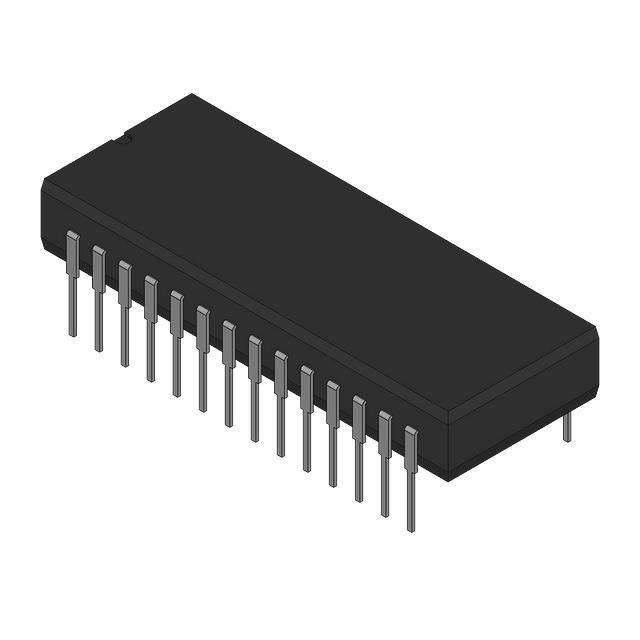


 工商网监
湘ICP备2023018690号
工商网监
湘ICP备2023018690号
