Available at Digi-Key**
www.digikey.com
OCXO
Specification
OX914xS3 Series
Features:
Description:
2111 Comprehensive Drive
Aurora, Illinois 60505
Phone: 630- 851- 4722
Fax: 630- 851- 5040
www.conwin.com
US Headquarters:
630-851-4722
European Headquarters:
+353-61-472221
Connor-Winfield model series
OX914xS3 is a 3.3 Vdc, Oven
Compensated Crystal Oscillator
(OCXO) in a 9x14 mm SMT package.
The OX914xS3 series is a low cost,
high performance OCXO that meets
STRATUM 3 requirements.
4
134 3
S
140 Z
OX9 .44 MH
19
• 3.3 Vdc Operation
• SMT Package
• Frequency Stability: +/-140 ppb
• Temperature Ranges Available:
0 to 70°C; -20 to 70°C; -40 to 85°C
• LVCMOS Output Logic
• Tape and Reel Packaging
• RoHS Compliant / Lead Free
Absolute Maximum Ratings
Parameter
Minimum
Storage Temperature
-55
Supply Voltage
-0.5
Operating Supply Voltage (Vcc)
3.135
Nominal
-
-
3.30
Maximum
85
5.5
3.465
Units
°C
Vdc
Vdc
Notes
Absolute Ratings: Stresses beyond those listed under "absolute maximum ratings" may cause permanent damage to the device.
These are stress ratings only. The functional operation of the device at those or any other conditions beyond those indicated under
"recommended operating conditions" is not implied. Exposure to conditions outside the "recommended operating conditions" for
any extended period of time may adversely impact device reliability and result in failures not covered by warranty.
Operating Specifications
Parameter
Minimum
Nominal
Maximum
Units
Notes
Frequencies Available: (Fo) 10, 12.8,13, 19.2, 19.44, 20, 26
MHz
Freq. Calibration @ 25°C
-1.0
-
1.0
ppm 1
Freq. Stability vs. Temperature
-140
-
140
ppb 2
Daily Aging
-40
-
40
pbb 3
Holdover Stability:
-320
-
320
ppb 4
MTIE
-
-
1E-6 5
Aging per Year
-300
-
300
ppb 3
Freq. Stability vs. Supply Voltage
-20
-
20
ppb (+/-5%)
Freq. Stability vs. Load Change
-10
-
10
ppb (+/-10%)
Short Term Stability
-
-
1.0E-9/s
Total Frequency Tolerance (20 Years) -4.6
-
4.6
ppm 6
Operating Temperature Range: (See Ordering Information.)
Models OX9140S3
0
-
70
°C
Models OX9142S3
-20
-
70
°C
Models OX9143S3
-40
-
85
°C
Supply Voltage: (+/-5%) (Vcc)
3.135
3.30
3.465
Vdc
Power Consumption: Turn On
-
-
3.00
W
Power Consumption: Steady State
-
-
1.30
W
Start-up Time
-
-
10
ms
Warm Up Time (Within Specification @ 25°C)
-
60
s
Warm Up Time (Within Specification @ -40 C)
-
90
s
LVCMOS Output Characteristics
Bulletin
Page
Revision
Date
Cx181
1 of 4
05
17 Sep 2013
Parameter
Minimum
Load
-
Output Voltage: High (Voh)
2.7
Low (Vol)
-
Drive Current: High (Ioh)
-
Low (Iol)
-
Duty Cycle at 50% of Vcc
45
Rise / Fall Time: 10% to 90%
-
Phase Jitter (BW=12KHz to Fo/2)
-
Typical Phase Noise for Fo = 10.0 MHz
SSB Phase Noise at 1Hz offset
-
SSB Phase Noise at 10Hz offset -
SSB Phase Noise at 100Hz offset -
SSB Phase Noise at 1KHz offset -
SSB Phase Noise at 10KHz offset -
SSB Phase Noise at 100KHz offset -
Nominal
15
-
-
-
-
50
-
0.5
Maximum
-
-
0.3
-4
4
55
6.5
1
-65
-105
-130
-148
-153
-155
-
-
-
-
-
-
Units
Notes
pF 7
Vdc
Vdc
mA
mA
%
ns
ps rms
dBc/Hz
dBc/Hz
dBc/Hz
dBc/Hz
dBc/Hz
dBc/Hz
Package Characteristics
OX914 Package Package consisting of a FR-4 substrate and Ryton-R-4 cover. Water Resistant
package, non-hermetic seal. (Engineering Properties of Ryton R-4 Application Note AN2100)
�2111 Comprehensive Drive
Aurora, Illinois 60505
Phone: 630- 851- 4722
Fax: 630- 851- 5040
www.conwin.com
Environmental Characteristics
Shock
500 G’s 1ms, Halfsine, 3 shocks per direction, per MIL-STD 202G, Method 213B Test Condition D.
Sinusoidal Vibration
0.06” D.A. or 10G’s Peak, 10 to 500 Hz, per MIL-STD-202G, Method 204D, Test Condition A.
Random Vibration
5.35 G’s rms. 20 to 2000 Hz per MIL-STD-202G, Method 214,Test Condition 1A, 15 minutes each axis.
Moisture
10 cycles, 95% RH, Per MIL-STD-202G, Method 112.
Marking Permanency
Per MIL-STD-202G, Method 215J.
Solder Process Recommendations: RoHS compliant, lead free. See solder profile on page 3.
In-line reflow:
Refer to recommended reflow pre-heat and reflow temperatures on page 6. Package material
consist of Ryton R-4 high temperature cover with FR4 substrate. Component solder is Pb free
high temperature eutectic alloy with a melting point of 221°C.|
In-line oven profile:
We recommend using KIC profiler or similar device placing one of the thermocouples on the
device to insure that the internal package temperature does not exceed 221°C.
Removal of device:
If for any reason the device needs to be removed from the board, use a temperature controlled
repair station with profile monitoring capabilities. Following a monitored profile will insure the
device is properly pre-heated prior to relow. Refer to IPC 610E for inspection guidelines.
Recommended Cleaning Process: (If required)
Device is non-hermetic, water resistance with four weep holes, one in each corner to allow
moisture to be removed during the drying cycle. We recommend in-line warm water wash
with air knife and drying capabilities. If cleaner does not have drying capability, then use hot air
circulated oven. Boards should be placed in the oven vertically for good water runoff
Device must be dried properly prior to use!
Note: If saponifier is used make sure the device is rinsed properly to insure all residues are removed. PH of saponifier should not exceed 10.
Drying Temperature:
Between 85 to 100°C.
Drying Time:
Time will vary depending on the board size.
Caution: Do not submerge the device!
Notes:
1. Initial calibration @ 25°C.
2. Frequency stability vs. change in temperature. [±(Fmax - Fmin)/(2*Fo)].
3. After 30 days of operation.
4. Peak to peak frequency stability vs. change in temperature, frequency stability vs. change in voltage, frequency stability vs. change in load and aging
over a 24 hour period.
5. 0.16 seconds < Observed time < 64 seconds at a constant temperature with 1 hour warm-up.
6. Inclusive of calibration @ 25°C, frequency vs. change in temperature, change in supply voltage (±5%), load change (±10%), shock and vibration and
20 years aging
7. Attention: To achieve optimal frequency stability, and in some cases to meet the specification stated on this data sheet, it is required that the circuit
connected to this OCXO output must have the equivalent input capacitance that is specified by the nominal load capacitance. Deviations from the
nominal load capacitance will have a graduated effect on the stability of approximately 20 ppb per pF load difference.
Ordering Information
** Not all options
available at
Digi-Key
OX914
0
S3
-019.44M
Oscillator Type
Temperature Range
STRATUM 3
OX914xxx - OCXO
9x14mm Package
0 = 0 to 70°C
2 = -20 to 70°C
3 = -40 to 85°C
S3
Output Frequency
Frequency Format
-xxx.xM Min.*
-xxx.xxxxxxM Max*
Example Part Number:
OX9140S3-019.44M = OCXO, 9x14mm package, 0 to 70°C, STRATUM 3, 19.44 MHz
*Amount of numbers after the
decimal point. M = MHz
Attention: System Designers please review Application Note AN2093:
System Design Information and Printed Circuit Board Layout Guidelines for OCXO Oscillators.
@ www.conwin.com/technologies.html
Specifications subject to change without notification. See Connor-Winfield's website for latest revision. All dimensions in inches.
© Copyright 2014 The Connor-Winfield Corporation Not intended for life support applications.
Bulletin
Page
Revision
Date
Cx181
2 of 4
05
17 Sep 2013
�2111 Comprehensive Drive
Aurora, Illinois 60505
Phone: 630- 851- 4722
Fax: 630- 851- 5040
www.conwin.com
Package Outline
A
b
0.290
(7.37mm)
L
DNC
CL
Marking
D
e
Pin 1
Index
Top View
Side View
A1
Side View
4
3
1
1344
OX9140S3
19.44 MHz
DNC
E
CL
Suggested Pad Layout
Symbol
A
D
E
A1
L
b
e
Min
8.89
13.34
-
Top 2
5
View
0.100
(2.54mm)
Pin 1 ID
6
Bottom View
DNC = Do Not Connect
mm
Nom. Max.
7.92
9.02 9.15
13.47 13.60
2.36
1.52
1.02
2.54
-
Min
0.350
0.545
-
CMOS Output Waveform
inches
Nom.
0.355
0.550
0.093
0.060
0.040
0.100
0.060
(1.52mm)
1
0.085
(2.03mm)
Max.
0.312
0.360
0.555
-
Keep Out Area
Keep Out Area Note: Do not route any traces
under the device in the keep out area.
Test Circuit
Pad Connections
DNC
Output
10uF
to
100 uF
0.01uF
2
15 pF
1: N/C
2: Do Not Connect
3 Ground:
4: Output
5: Do Not Connect
6: Supply Voltage (Vcc)
DNC
N/C
DNC = Do Not Connect
DO NOT connect "DNC" pads
to ground or supply rails.
*DO NOT connect "DNC" pads
to ground or supply rails.
1V/Div
Phase Noise Plot
Typical Phase noise for OX9140S3-010.0M
Solder Profile
Temperature
260°C
260°C
220°C
180°C
150°C
120°C
0
10 s
Up to 120 s
60 to 90 s
Typical
Typical
Meets IPC/JEDEC J-STD-020C
Bulletin
Page
Revision
Date
Specifications subject to change without notification. See Connor-Winfield's website for latest revision. All dimensions in inches.
© Copyright 2014 The Connor-Winfield Corporation Not intended for life support applications.
Cx181
3 of 4
05
17 Sep 2013
�2111 Comprehensive Drive
Aurora, Illinois 60505
Phone: 630- 851- 4722
Fax: 630- 851- 5040
www.conwin.com
Tape and Reel Information
CW
0926
OX9140S3
19.44 MHZ
SM-MECH42
Revision History
Revision
00
01
02
03
04
05
Date
09/22/10
01/20/11
04/22/11
05/25/11
05/07/13
09/17/13
Description
Data sheet released
Added tape and reel information to the data sheet
Added frequency stability note and Recommended Cleaning Process
Updated specifications
Updated Environmental Characteristics
Updated package drawing and suggested layout to IPC
Bulletin
Page
Revision
Date
Specifications subject to change without notification. See Connor-Winfield's website for latest revision. All dimensions in inches.
© Copyright 2014 The Connor-Winfield Corporation Not intended for life support applications.
Cx181
4 of 4
05
17 Sep 2013
�
很抱歉,暂时无法提供与“OX9143S3-010.0M”相匹配的价格&库存,您可以联系我们找货
免费人工找货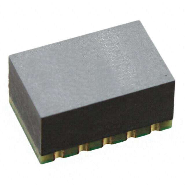


 工商网监
湘ICP备2023018690号
工商网监
湘ICP备2023018690号
