Available at Digi-Key
Low Jitter
V7223T Series
LVCMOS VCXO
www.digikey.com
2111 Comprehensive Drive
Aurora, Illinois 60505
Phone: 630- 851- 4722
Fax: 630- 851- 5040
Description
Features:
The Connor-Winfield V7223T Series models
are 3.3V SMT 5.0x3.2mm voltage controlled
crystal oscillators (VCXOs) with ultra low jitter. With LVCMOS outputs, the V7223T series
is designed for PLL applications requiring high
performance and low noise.
• 3.3V Operation
• Low Jitter 60fs RMS typical
• Absolute Pull Range: ±50ppm
• Pin 1 Input Impedance 10M ohm
• 5.0x3.2mm Surface Mount Package
• Tape and Reel Packaging
• RoHS Compliant / Lead Free
www.conwin.com
US Headquarters:
630-851-4722
European Headquarters: +353-61-472221
Absolute Maximum Ratings
Parameter
Storage Temperature
Supply Voltage (Vdd)
Control Voltage (Vc)
Minimum
Nominal
Maximum
Units
-55
-0.5
-0.5
-
-
-
125
4.6
Vdd+0.5
°C
Vdc
Vdc
Notes
Operating Specifications
Parameter
Minimum
Center Frequency (Fo)
50
Operating Temperature Range
-40
Supply Voltage (Vdd)
3.135
Supply Current (Idd)
-
Period Jitter RMS
-
Integrated Phase Jitter (BW=12kHz to 20MHz)
Fo=80MHz
Fo=100MHz
Fo=125MHz
Fo=156.25MHz
Typical Phase Noise for 100MHz
SSB Phase Noise at 10Hz offset
SSB Phase Noise at 100Hz offset
SSB Phase Noise at 1kHz offset
SSB Phase Noise at 10kHz offset
SSB Phase Noise at 100kHz offset
SSB Phase Noise at 1MHz offset
SSB Phase Noise at 10MHz offset
-
-
-
-
-
-
-
Nominal
Maximum
Units
-
-
3.3
-
3
156.25
85
3.465
25
5
MHz
°C
Vdc
mA
ps RMS
100
60
60
60
fs RMS
fs RMS
fs RMS
fs RMS
-70
-105
-130
-148
-158
-163
-164
-
-
-
-
-
-
-
dBc/Hz
dBc/Hz
dBc/Hz
dBc/Hz
dBc/Hz
dBc/Hz
dBc/Hz
Notes
Input Characteristics
Parameter
Control Voltage Range (Vc)
Typical Slope (Vc=1.65Vdc)
Absolute Pull Range (APR)
Fo = 50MHz to 125MHz
Fo >125MHz
Monotonic Linearity
DC Input Resistance (Pad 1)
Modulation Bandwidth (3dB)
Enable / Disable Function (O/E)
Enable Input Voltage - High (Vih)
Disable Input Voltage - Low (Vil)
Minimum
Nominal
Maximum
Units
0.3
1.65
3.0
Vdc
Notes
-
65
-
ppm/V
±50
±30
-10
-
25
-
-
-
10M
-
-
-
10
-
-
ppm
ppm
%
Ohm
kHz
1
1
2.4
-
-
-
-
0.4
Vdc
2
Notes
LVCMOS Output Characteristics
Parameter
Load
Voltage High (Voh)
Low (Vol)
Duty Cycle at 50% Level
Rise / Fall Time 20% to 80%
Bulletin
Page
Revision
Date
Vx673
1 of 3
03
24 Nov 2020
Notes:
Minimum
Nominal
Maximum
Units
-
0.9*Vdd
-
45
-
-
-
-
50
0.5
15
-
0.1*Vdd
55
2.0
pF
Vdc
Vdc
%
nS
1. Absolute pull range (APR) is the minimum guaranteed pull range of the VCXO under all conditions over the lifetime operation.
Including calibration @ 25°C, frequency vs. change in temperature, frequency vs. change in supply voltage, frequency vs. change in
load, shock and vibration and aging for ten years. The APR is referenced to Fo. Positive Transfer Function.
2. Output is enabled with no connection on Pad 2. When oscillator is disabled the output is high impedance.
�2111 Comprehensive Drive
Aurora, Illinois 60505
Phone: 630- 851- 4722
Fax: 630- 851- 5040
www.conwin.com
Package Characteristics
Package Hermetically sealed, ceramic package with grounded metal cover.
Soldering Process RoHS compliant / lead free, see solder profile on page 3.
Typical Phase Noise V7223T-100.0M
Ordering Information
V7223T - 050.0M
V7223T - 080.0M
V7223T - 098.304M
V7223T - 100.0M
V7223T - 122.88M
V7223T - 125.0M
V7223T-148.5M
V7223T-155.52M
V7223T-156.25M
Package Layout
Enable / Disable Function
Enable / Disable Function (Pad 2)
No Connection
High
Low
Output
Enable
Enable
Disable (High Impedance)
Pad Connections
Suggested Pad Layout
Pin Function
1: Control Voltage
2: Output Enable (OE)
3: Ground
4: Output
5: N/C
6: Vdd
Bulletin
Page
Dimensional Tolerance ±0.13mm
Revision
Date
Specifications subject to change without notification. See Connor-Winfield's website for latest revision.
© Copyright 2020 The Connor-Winfield Corporation Not intended for life support applications.
Vx673
2 of 3
03
24 Nov 2020
�2111 Comprehensive Drive
Aurora, Illinois 60505
Phone: 630- 851- 4722
Fax: 630- 851- 5040
www.conwin.com
Test Circuit
Output Waveform
Tape and Reel Dimensions
Solder Profile
Temperature
PIN 1
.53
(13.5mm)
8.46 DIA
(215mm DIA)
.08
(2.0mm)
.217
.08
260°C
260°C
220°C
180°C
(5.5mm)
150°C
(2.0mm)
120°C
.15
(3.7mm)
9.84 DIA
(250mm DIA)
.157
0
(4.0mm)
.08
(2.0mm)
3.15
(8.0mm)
10 s
Up to 120 s
60 to 90 s
Typical
Typical
3.15
(8.0mm)
.06 DIA
(1.5mm DIA)
1.00 DIA
(25mm DIA)
Meets IPC/JEDEC J-STD-020C
Dimensional Tolerance:
±.02" (.508mm)
±.005" (.127mm)
.217 (5.5mm)
MEETS EIA-481A and EIAJ-1009B
2,000 PCS/REEL
.07 (1.75mm)
.47 (12.0mm)
Bulletin
Page
Revision
Date
Specifications subject to change without notification. See Connor-Winfield's website for latest revision.
© Copyright 2020 The Connor-Winfield Corporation Not intended for life support applications.
Vx673
3 of 3
03
24 Nov 2020
�
很抱歉,暂时无法提供与“V7223T-050.0M”相匹配的价格&库存,您可以联系我们找货
免费人工找货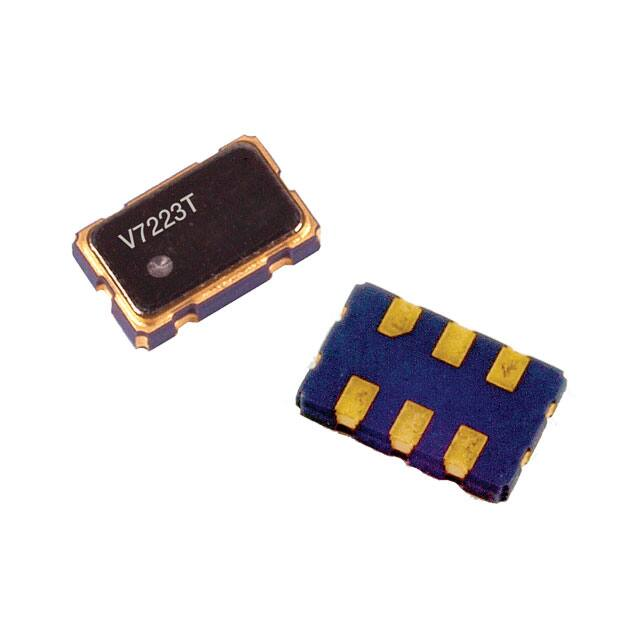


 工商网监
湘ICP备2023018690号
工商网监
湘ICP备2023018690号
