MAX11253/MAX11254 Family
Evaluation Kit
General Description
The MAX11253/MAX11254 evaluation kit (EV kit) provides a proven design to evaluate the MAX11253/
MAX11254 family of 16-bit/24-bit, 6-channel, 64ksps,
integrated PGA delta-sigma ADCs. The EV kit includes
a graphical user interface (GUI) that provides communication from the target device to the PC. The EV kit can
operate in multiple modes:
1) Standalone Mode: in “standalone” mode, the EV
kit is connected to the PC via a USB cable and
performs a subset of the complete EV kit functions
with limitations for sample rate, sample size, and no
support for coherent sampling.
2) FPGA Mode: in “FPGA” mode, the EV kit is
connected to an Avnet ZedBoard™ through a lowpin-count FMC connector. ZedBoard features a
Xilinx® Zynq® -7000 SoC, which connects to the
PC through an Ethernet port, allowing the GUI to
perform different operations with full control over
mezzanine card functions. The EV kit with FPGA
platform performs the complete suite of evaluation
tests for the target IC.
3) User-Supplied SPI Mode: In addition to the USB and
FMC interfaces, the EV kit provides a 12-pin Pmod™style header for user-supplied SPI interface to connect the signals for SCLK, DIN, DOUT, and CNVST.
The EV kit includes Windows XP®, Windows® 7, and
Windows 8.1-compatible software for exercising the features of the IC. The EV kit GUI allows different sample
sizes, adjustable sampling rates, internal or external reference options, and graphing software that includes the
FFT and histogram of the sampled signals.
The ZedBoard accepts a +12V AC-DC wall adapter. The
EV kit can be powered by a local +12V supply. The EV kit
has on-board transformers and digital isolators to separate the IC from the ZedBoard/on-board processor.
The MAX11253/MAX11254 EV kit comes installed with a
MAX11253ATJ+ or MAX11254ATJ+ in a 32-pin TQFN-EP
package.
19-7584; Rev 2; 4/18
Evaluates: MAX11253/MAX11254
Features
●● High-Speed USB Connector, FMC Connector, and
Pmod-Style Connector
●● 8MHz SPI Clock Capability through FMC Connector
●● 8MHz SPI Clock Capability in Standalone Mode
●● Various Sample Sizes and Sample Rates
●● Collects Up to 1 Million Samples
(with FPGA Platform)
●● Time Domain, Frequency Domain, and Histogram
Plotting
●● Sync In and Sync Out for Coherent Sampling
(with FPGA Platform)
●● On-Board Input Buffers: MAX9632 and MAX44205
(Fully Differential)
●● On-Board Voltage References
(MAX6126 and MAX6070)
●● Proven PCB Layout
●● Fully Assembled and Tested
●● Windows XP-, Windows 7-, and Windows
8.1-Compatible Software
Ordering Information appears at end of data sheet.
Pmod is a trademark of Digilent Inc.
ZedBoard is a trademark of Avnet, Inc.
Xilinx and Zynq are registered trademarks and Xilinx is a registered service mark of Xilinx, Inc.
Windows and Windows XP are registered trademarks and registered service marks of Microsoft Corporation.
�MAX11253/MAX11254 Family
Evaluation Kit
Evaluates: MAX11253/MAX11254
MAX11253/11254 EV Kit Photo
www.maximintegrated.com
Maxim Integrated │ 2
�MAX11253/MAX11254 Family
Evaluation Kit
Evaluates: MAX11253/MAX11254
System Block Diagram
MAX11253/MAX11254 EV Kit Files
FILE
DECRIPTION
MAX11253_54EVKitSetupV1.0.exe
Application Program
(GUI)
Note: In the following section(s), software-related items
are identified by bolding. Text in bold refers to items directly from the EV system software. Text in bold and underline refers to items from the Windows operating system.
Boot.bin
ZedBoard firmware
(SD card to boot
Zynq)
The EV kit is fully assembled and tested. Follow the steps
below to verify board operation:
Quick Start
Required Equipment
●●
MAX11253/MAX11254 EV kit
●●
+12V (500mA) power supply
●●
Micro-USB cable
●●
ZedBoard FPGA platform
(optional – NOT INCLUDED with EVKit)
●●
Function generator (optional)
●●
Windows XP, Windows 7, or Windows 8.1 PC with a
spare USB port
www.maximintegrated.com
Procedure
1) Visit http://www.maximintegrated.com/evkitsoftware to download the latest version of the EV kit software, MAX11253_54EVKITSetupV1.0.zip. Save the
EV kit software to a temporary folder and uncompress
the ZIP file.
2) Install the EV kit software and USB driver on your
computer by running the MAX11253_54EVKitSetupV1.0.exe
program inside the temporary folder. The program
files are copied to your PC and icons are created in
the Windows Start | Programs menu. At the end of
the installation process the installer will launch the installer for the FTDIChip CDM drivers.
Maxim Integrated │ 3
�Evaluates: MAX11253/MAX11254
MAX11253/MAX11254 Family
Evaluation Kit
For Standalone mode:
1) Verify that all jumpers are in their default positions for
the EV kit board (Table 2).
2) Connect the PC to the EV kit using a micro-USB cable.
3) Connect the +12V adapter to the EV kit.
4) Start the EV kit software by opening its icon in the
Start | Programs menu. The EV kit software appears
as shown in Figure 1. From the Device menu select
Standalone. Verify that the lower left status bar indicates the EV Kit hardware is Connected.
For FPGA mode (when connected to a Zedboard):
1) Connect the Ethernet cable from the PC to the ZedBoard and configure the Internet Protocol Version
4 (TCP/Ipv4) properties in the local area connection to IP address 192.168.1.2 and subnet Mask to
255.255.255.0.
7) Start the EV kit software by opening its icon in the
Start | Programs menu. The EV kit software appears
as shown in Figure 1. From the Device menu select
FPGA. Verify that the lower left status bar indicates
the EV Kit hardware is Connected.
For Either Standalone or FPGA Mode:
1) Connect the positive terminal of the function generator to the AIN0D+ (TP1) test point on the EV kit. Connect the negative terminal of the function generator to
the AIN0D- (TP2) test point on the EV kit.
2) Configure the signal source to generate a 100Hz,
1VP-P sinusoidal wave with +1V offset.
3) Turn on the function generator.
4) In the Device menu, choose either standalone or the
FPGA option. In the configuration group, select Channel 0 and click Convert in the serial interface menu.
5) Click on the Scope tab.
2) Verify that the ZedBoard SD card contains the Boot.
bin file for the MAX11253/MAX11254 EV kit.
6) Check the Remove DC Offset checkbox to remove
the DC component of the sampled data.
3) Connect the EV kit FMC connector to the ZedBoard
FMC connector. Gently press them together.
7) Click the Capture button to start the data analysis.
4) Verify that all jumpers are in their default positions for
the ZedBoard (Table 1) and EV kit board (Table 2).
9) Verify that the frequency, which is displayed on the
right, is approximately 100Hz. The scope image has
buttons in the upper right corner that allow zooming
in to detail.
5) Connect the 12V power supply to the ZedBoard.
Leave the Zedboard powered off.
8) The EV kit software appears as shown in Figure 1.
6) Enable the ZedBoard power supply by sliding SW8 to
ON and connect the +12V adapter to the EV kit.
Table 1. ZedBoard Jumper Settings
JUMPER
SHUNT POSITION
J18
1-2
VDDIO set for 3.3V.
JP11
JP10
JP9
JP8
JP7
2-3
1-2
1-2
2-3
2-3
Boot from SD Card
J12
NA
SD Card installed
J20
NA
Connected to 12V wall adapter
SW8
OFF
www.maximintegrated.com
DESCIPTION
ZedBoard power switch, OFF while connecting boards
Maxim Integrated │ 4
�MAX11253/MAX11254 Family
Evaluation Kit
Evaluates: MAX11253/MAX11254
Table 2. MAX11253/MAX11254 Board Jumper Settings
HEADER
JMP1
J8
J10
J11
J12
J13
JUMPER
POSITION
1-2*
Use MAX6126 3.0V as VREF
signal
1-3
Use MAX6070 3.0V as VREF
signal
1-4
Use MAX6070 1.8V as VREF
signal
Open*
Generate +3.3V for DVDD
1-2
Generate +2.0V for DVDD
1-2*
Select +3.3V or +2.0V as DVDD
2-3
Select +1.8V as DVDD
Open*
U1 uses internal clock
1-2
External clock from FPGA
2-3
External clock from U10
1-2*
Select +3.3V as AVDD
2-3
Select +1.8V as AVDD
1-2*
Select AVSS as REFN
2-3
Select REFN_S from J1 as
REFN for external sense point
Open*
J14
1-2
J15
Open*
HEADER
1-2*
Select REFP_F signal as REFP
input
2-3
Select REFP_S signal from J1
as REFP input
1-2*
Use AGND as AVSS. Use this
setting if AVDD is +3.3V
2-3
Use -1.8V as AVSS. Use this
setting if AVDD is +1.8V
1-2*
Use VREF as REFP_F
2-3
Use AVDD as REFP_F
1-2*
Short AIN2.1- (J27, TP38) to
AGND and for U11 noninverting
configuration
J37
3-4*
Short AIN2.1+ (J28, TP39) to
AGND and for U11 inverting
configuration
J38
J31
www.maximintegrated.com
3-4*
Short AIN2.3+ (J30, TP43) to
AGND and for U12 inverting
configuration
1-2*
Short AIN2.2- (TP40) to AGND
and for U13 noninverting
configuration
3-4*
Short AIN2.2+ (TP41) to
AGND and for U13 inverting
configuration
1-2*
Short AIN2.4- (TP44) to AGND
and for U14 noninverting
configuration
3-4*
Short AIN2.4+ (TP45) to
AGND and for U14 inverting
configuration
1-2*
Connect output of U11 to
inverting input of U13
3-4
Connect AIN2.2- (TP40) to
inverting input of U13
5-6
Connect output of U11 to
noninverting input of U13
7-8*
Connect AIN2.2+ (TP41) to
noninverting input of U13
1-2*
Connect output of U12 to
inverting input of U14
3-4
Connect AIN2.4- (TP44) to
inverting input of U14
5-6
Connect output of U12 to
noninverting input of U14
7-8*
Connect AIN2.4+ (TP45) to
noninverting input of U14
J35
Use external SYNC signal
J17
Short AIN2.3- (J29, TP42) to
AGND and for U12 noninverting
configuration
J34
Use TP23 as GPIO1
DESCRIPTION
1-2*
J33
Use internal 1.8V subregulator if
DVDD ≥ 2.0V
Use DVDD for internal logic if
DVDD ≤ 2.0V
JUMPER
POSITION
J32
1-2
J16
J24
DESCRIPTION
J36
Open*
No offset to U13 noninverting
input
1-2
Offset U13 output by VREF/2
Open*
No offset to U14 noninverting
input
1-2
Offset U14 output by VREF/2
Maxim Integrated │ 5
�MAX11253/MAX11254 Family
Evaluation Kit
Evaluates: MAX11253/MAX11254
Table 2. MAX11253/MAX11254 Board Jumper Settings (continued)
HEADER
JUMPER
POSITION
1-2*
Short AIN3.1- (TP56) to AGND
and for U15 noninverting
configuration
3-4*
Short AIN3.1+ (TP57) to
AGND and for U15 inverting
configuration
1-2*
Short AIN3.3- (TP60) to AGND
and for U16 noninverting
configuration
J39
J40
3-4*
Short AIN3.3+ (TP61) to
AGND and for U16 inverting
configuration
1-2*
Short AIN3.2- (TP58) to AGND
and for U17 noninverting
configuration
J41
3-4*
Short AIN3.2+ (TP59) to
AGND and for U17 inverting
configuration
1-2*
Short AIN3.4- (TP62) to AGND
and for U18 noninverting
configuration
3-4*
Short AIN3.4+ (TP63) to
AGND and for U18 inverting
configuration
1-2*
Connect output of U15 to
inverting input of U17
3-4
Connect AIN3.2- (TP58) to
inverting input of U17
5-6
Connect output of U15 to
noninverting input of U17
7-8*
Connect AIN3.2+ (TP59) to
noninverting input of U17
1-2*
Connect output of U16 to
inverting input of U18
3-4
Connect AIN3.4- (TP62) to
inverting input of U18
5-6
Connect output of U16 to
noninverting input of U18
7-8*
Connect AIN3.4+ (TP63) to
noninverting input of U18
J42
J43
J44
J45
DESCRIPTION
Open*
No offset to U17 noninverting
input
1-2
Offset U17 output by VREF/2
www.maximintegrated.com
HEADER
J46
JUMPER
POSITION
Open*
No offset to U18 noninverting
input
1-2
Offset U18 output by VREF/2
1-2*
Short AIN4+ (J47, TP72) to
AGND
3-4*
Short AIN4- (J48, TP73) to
AGND
1-2*
Short AIN5+ (TP74) to AGND
3-4*
Short AIN5- (TP75) to AGND
J49
J50
J63
J64
Open*
Use external +12V source
1-2
Use +12V from ZedBoard
Open
If connected to ZedBoard FPGA
1-2*
If connected to PC through USB
interface
1-2*
Enable U28 H-bridge transformer
driver to use onboard ±15V
supply generation
2-3
Disable U28 and use and
external ±15V supply to TP83,
TP86, and TP87
1-2
Use an external -15V power
supply, connected to TP86
3-4*
Use U28 driver to generate
isolated -15V
1-2
Use an external +15V power
supply, connected to TP83
3-4*
Use U28 driver to generate
isolated +15V
1-2
Use an external +12V power
supply to TP91 as VCC
3-4*
Use onboard +12V from U32
LDO as VCC
1-2
AGND as VEE
3-4
Use an external -12V power
supply to TP90 as VEE
5-6*
Use onboard -12V from U33
LDO as VEE
J65
J66
J67
J68
J69
DESCRIPTION
*Default configuration
Maxim Integrated │ 6
�MAX11253/MAX11254 Family
Evaluation Kit
General Description of Software
The main window of the EV kit software contains seven
tabs: Configuration, Scope, DMM, Histogram, FFT, Scan
Mode, and Registers. The Configuration tab provides
control for the ADC configuration including calibration and
data capture. The other six tabs are used for evaluating
the data captured by the ADC.
Configuration Tab
The Configuration tab provides an interface for selecting
and configuring the ADC from a functional perspective.
Select the desired Device for either Standalone or FPGA
in the dropdown menu and the corresponding properties
of the device are displayed including Channel number,
Sample Rate, Number of Samples, Reference Voltage,
Sequencing Mode, Calibration, GPO/GPIO selection, Input Path (Direct or internal PGA), Delta-Sigma
Modulator type selection for different Data Format and
Conversion Mode, Serial Interface function (Convert,
and Read All), Power setting (NOP, Power Down, and
Evaluates: MAX11253/MAX11254
Standby), Reset Registers, and RSTB Reset, Clock/
SYNC (Internal or External Clock, and Disable or Enable
SYNC Mode), and Other for Disable or Enable Current
Sink/Source and CAPREG LDO.
The sample settings are available on the left of the configuration menu, which allow the user to select the Channel,
Sample Rate, Number of Samples and Clock Source if
FPGA device is used.
The Read Data and Status information is displayed on
the right, which shows the data in both voltage and Hex,
the sample rate, and power state for the selected channel. In addition, if there are any errors, the indicator lights
will turn red.
Channel Selection
To select the desired channel among the six available
channels, click Channel # dropdown menu at the top left
and select the desired channel from 0 to 5. The default
selection is Channel 0.
Figure 1. EV Kit Software (Configuration Tab)
www.maximintegrated.com
Maxim Integrated │ 7
�Evaluates: MAX11253/MAX11254
MAX11253/MAX11254 Family
Evaluation Kit
Sample Rate (SPS)
To select the desired data rate for single-cycle mode from
50sps to 12800sps and for continuous mode data rate
from 1.9sps to 64000sps, choose the Sample Rate (SPS)
from the dropdown menu below the Channel # selection.
Three conversion modes are provided: Continuous,
Single Cycle, and Single Continuous. Click the
Conversion Modes dropdown menu under the DeltaSigma Modulator section to select the desired conversion mode.
Reference Voltage
Serial Interface
There are three different reference voltages available
on board: MAX6070AUT18+ (1.8V), MAX6070AUT30+
(3.0V), and MAX6126AASA30+ (3.0V). To select 1.8V,
place JMP1 from position 1 to 4. To select 3.0V MAX6070
with ±0.04% accuracy, place JMP1 from position 1 to 3. To
select 3.0V MAX6126 with ±0.02% accuracy, place JMP1
from position 1 to 2.
Power
Sequencer Mode
To change the sequencer mode, click the Sequence
Mode selection below the Sequencing menu and select
Mode 1, 2, or 3 as desired. Check the GPO Sequencer
Mode box to enable GPO/GPIO function in mode 3. In
addition, check the Enable box to enable the MUX and
GPO Delay. Choose the desired delay in microseconds
by clicking on the + or – buttons.
ADC Calibration
Two types of software calibration for offset and gain are
available: Self calibration and system calibration.
The primary mode for calibration is using the dropdown
list to select a calibration mode, followed by clicking the
Calibrate button. The checkboxes for Self Offset, Self
Gain, System Offset, and System Gain allow for the
user to enable or disable the calibration values. The calibration values can also be changed manually by entering
a hex value in the numeric box.
To starting converting, click the Convert button under
the Serial interface section. To read all registers, click the
Read All button.
The MAX11253/MAX11254 EV kit features three powerdown states: Normal Operating Power (NOP), Power
down, and Standby. Select the desired power state by
clicking the drop-down menu under the Power section.
To reset the configuration settings back to default values,
press the Reset Registers button.
To exercise the power-on reset feature, click the RSTB
button.
Clock/SYNC
The internal clock mode is set at default condition. To
use the external clock provided on-board, select External
under the Clock/SYNC section and install jumper J11
from 2-3. To user-supplied external clock, select External
under the Clock/SYNC section and install jumper J11
from 1-2. In addition, the Sync mode can be enabled
or disabled by clicking the drop-down menu under this
Clock/SYNC section and install jumper J15. The Sync
signal should be provided externally.
Other
To select GPO or GPIO ports, choose the option under the
GPO/GPIO dropdown menu and check the Enable box.
To enable (J14 open) or disable (J14 installed and VDDVD
≤ 2.0V) the internal CAPREG LDO for digital and I/O supply, select this option from the drop-down menu under
the Other section. Additionally, Current Sink/Source can
also be disabled or enabled under this section.
Input Path
Read Data and Status
GPO/GPIO
Select Direct under the Input Path dropdown menu to
bypass the internal amplifiers and apply the analog input
signals directly to the MAX11253/MAX11254 inputs or to
use the external amplifiers.
Select PGA under the Input Path dropdown menu to use
the internal programmable gain amplifiers.
Delta-Sigma Modulator
To select the desired data format, click the Data Format
dropdown menu under the Delta-Sigma Modulator
section and choose either Bipolar or Unipolar with two’s
complement or offset binary options.
www.maximintegrated.com
The Read Data and Status on the far right hand side of
this Configuration menu depicts the received data and
status of the device such as the selected channel, data
rate, sample rate, and power state. Click the Read Data
and Status button to view the updated status.
To save a configuration, select Save ADC Config As… in
the File menu. This saves all the ADC register values to a
XML file. To load a configuration, select Load ADC Config
in the File menu. When the XML file is loaded, all the register values in the file are written to the ADC.
Maxim Integrated │ 8
�MAX11253/MAX11254 Family
Evaluation Kit
Scope Tab
The Scope tab sheet is used to capture data and display it
in the time domain. The desired Channel #, Sample Rate,
Number of Samples, Display Unit, Average Samples,
and Resolution Selection can also be set in this tab if
they were not appropriately adjusted in other tabs. The
Display Unit drop-down list allows counts in LSB and
voltages in V, mV, or µV. Once the desired configuration is
Evaluates: MAX11253/MAX11254
set, click on the Capture button. The right side of the tab
sheet displays details of the waveform, such as average,
standard deviation, maximum, minimum, and fundamental frequency as shown in Figure 2.
To save the captured data to a file, select Options > Save
Graph > Scope. This saves the setting on the left and the
data captured to a CSV file.
Figure 2. EV Kit Software (ScopeTab)
www.maximintegrated.com
Maxim Integrated │ 9
�MAX11253/MAX11254 Family
Evaluation Kit
DMM Tab
The DMM tab sheet provides the typical information as a
digital multimeter. Once the desired configuration is set,
Evaluates: MAX11253/MAX11254
click on the Capture button. Figure 3 displays the results
shown by the DMM tab when a 1.5V signal is applied to
AIN0+ and 1.0V to AIN0-.
Figure 3. EV Kit Software (DMM Tab)
www.maximintegrated.com
Maxim Integrated │ 10
�MAX11253/MAX11254 Family
Evaluation Kit
Histogram Tab
The Histogram tab sheet is used to show the histogram
of the data. Sample rate and number of samples can also
be set in this tab if they were not appropriately adjusted
in other tabs. Once the desired configuration is set, click
on the Capture button. The right side of the tab sheet
displays details of the histogram such as average, standard deviation, maximum, minimum, peak-to-peak noise,
effective resolution, and noise-free resolution as shown
in Figure 4.
Evaluates: MAX11253/MAX11254
The histogram tab is enabled at default. Using the histogram will slow down the GUI response. To disable it,
check the Disable Histogram box.
To save the histogram data to a file, go to Options > Save
Graph > Histogram. This saves the setting on the left
and the histogram data captured to a CSV file.
Figure 4. EV Kit Software (Histogram Tab)
www.maximintegrated.com
Maxim Integrated │ 11
�MAX11253/MAX11254 Family
Evaluation Kit
FFT Tab
The FFT tab sheet is used to display the FFT of the data.
The Sample Rate, Number of Samples, Resolution and
Window Function type can be set as desired. To calculate the Adjusted Input Signal frequency for Coherent
Sampling, enter the Input Signal frequency in Hertz and
push the Calculate button. Once the preferred configuration is set, click on the Capture button. The right side of
the tab displays the performance based on the FFT, such
as fundamental frequency, SNR, SINAD, THD, SFDR,
ENOB, and Noise Floor as shown in Figure 5.
Evaluates: MAX11253/MAX11254
To save the FFT data to a file, go to Options > Save
Graph > FFT. This saves the setting on the left and the
FFT data captured to a CSV file.
When coherent sampling is needed, this tab allows the
user to calculate the external clock frequency applied
to the board. Adjust the input frequency of the lowjitter clock to the value as shown in the Adjusted
Master Clock (Hz) and apply it to the EV KIT EXT_
CLK connector. See the Sync Input and Sync Output
section before using this feature.
Figure 5. EV Kit Software (FFT Tab)
www.maximintegrated.com
Maxim Integrated │ 12
�Evaluates: MAX11253/MAX11254
MAX11253/MAX11254 Family
Evaluation Kit
Figure 6 shows the setup Maxim Integrated uses to capture data for coherent sampling.
For coherent FFT evaluation, use the jumper settings
from Table 2 for proper configurations. The low-jitter clock
is synchronized with the signal generator at 10MHz from
the ZedBoard. To achieve coherent sampling, click on the
Calculate button and enter the Adjusted Master Clock
(Hz) frequency of approximately 8.192MHz into our lowjitter clock. Timing for all SPI timing and sampling rate are
based off the system clock.
LOW-JITTER CLOCK
RF_IN
8.192 MHz
OUT
ZedBoard
SIGNAL GENERATOR
RF_IN
PC
10MHz
-
INV-
+
INV+
EXT_CLK
MAX11253/MAX11254EVKIT
ETHERNET CABLE
Figure 6. EV Kit Coherent Sampling Setup
www.maximintegrated.com
Maxim Integrated │ 13
�MAX11253/MAX11254 Family
Evaluation Kit
Scan Mode Tab
The Scan Mode tab is used to perform selected data
conversions and read the converted data.
In the Sequence Setting section at the bottom, set the
desired sequencer mode (1 to 3) from the Sequence
Mode drop-down menu and select whether to assert
the RDYB pin after one channel or after scan completes options under the RDYB menu. Check the GPO
Sequencer Mode and Enable boxes as desired. Then
set the conversion time delay in µs for MUX and GPO by
clicking on the + or - buttons under the MUX Delay and
GPO Delay menu, allowing for high impedance source
networks to stabilize after the channels are selected.
Finally press the Read All button to view the selected
settings.
Evaluates: MAX11253/MAX11254
In the Read Data section on top, select the desired unit
in either LSB or voltage (V, mV, or µV) under the Display
Unit drop-down menu. Then choose the desired sample
rate by clicking on the Sample Rate drop-down menu
under. Finally, click the Scan button to start converting and press the Read Data button to view the converted data displayed on the right hand side as shown in
Figure 7.
Figure 7. EV Kit Software (Scan Mode Tab)
www.maximintegrated.com
Maxim Integrated │ 14
�Evaluates: MAX11253/MAX11254
MAX11253/MAX11254 Family
Evaluation Kit
ADC Registers Tab
The Registers tab sheet shows the device registers on
the left. The middle section shows the descriptions of the
selected register. Click Read All to read all registers and
refresh the window with the register settings. To write a
register first select the hex value in the Value column,
type the desired hex value and press Enter.
The command byte is on the right side of the tab sheet.
This byte precedes all SPI transactions and is described
in the IC datasheet. To send a command byte enter a
hex value in the numeric box and click the Send button.
The command byte has two different formats including Conversion Command and Register Read/Write.
Select the radio button for the desired mode to see the bit
description in the table. See Figure 8.
Detailed Description of Hardware
The MAX11253/MAX11254 EV kit provides a proven signal
path and board layout to demonstrate the performance of
the MAX11253/MAX11254 16-/24-bit, delta-sigma ADCs.
Included in the EV kit are digital isolators, isolated DC-DC
converters, ultra-low-noise LDOs to all supply pins of the
IC, on-board reference (MAX6126 and MAX6070), precision amplifiers (MAX9632 and MAX44205) for analog
inputs, and sync-in and sync-out signals for coherent
sampling.
An on-board FTDI controller is provided to allow for
evaluation in standalone mode, which has limitations on
maximum sample speed and on sample depth. The EV kit
can be used with FPGA to achieve full speed and a larger
sample depth.
The EV kit supports a number of different devices as
listed in Table 3.
Figure 8. EV Kit Software (ADC Registers Tab)
Table 3. Products Supported with MAX11253/MAX11254 EV Kit
PART NO.
RESOLUTION
MAX. SAMPLE RATE
MAX11253
16-bits
64ksps
MAX11254
24-bits
64ksps
www.maximintegrated.com
Maxim Integrated │ 15
�Evaluates: MAX11253/MAX11254
MAX11253/MAX11254 Family
Evaluation Kit
User-Supplied SPI
To evaluate the EV kit with a user-supplied SPI bus,
disconnect from the FMC bus and remove jumper J64.
Apply the user-supplied SPI signals to SCLK, CSB, DIN,
and DOUT at the PMOD_A header (J60). Make sure the
return ground is connected to PMOD ground.
The on-board FTDI chip used for standalone mode does
not conflict with the user-supplied SPI if it is powered off
by removing jumper J64.
CAUTION: DO NOT PLUG THIS HEADER INTO A
STANDARD PMOD INTERFACE FOUND ON OTHER
FPGA OR MICROCONTROLLER PRODUCTS. THE
SIGNAL DEFINITION IS UNIQUE TO THIS EV KIT.
FMC Interface:
The users should confirm compatibility of pin-usage between
their own FMC implementation and that of the Maxim
Integrated EV kit before connecting the Maxim Integrated
EV kit to a different system with FMC connectors.
Voltage References
There are three different reference voltages available
on board: MAX6070AUT18+ (1.8V), MAX6070AUT30+
(3.0V), and MAX6126AASA30+ (3.0V). To select 1.8V,
place JMP1 from position 1 to 4. To select 3.0V MAX6070
with ±0.04% accuracy, place JUMP1 from position 1 to
3. To select 3.0V MAX6126 with ±0.02% accuracy, place
JMP1 from position 1 to 2.
For user-supplied external references, remove jumper
J24 and connect a reference voltage to J24-2. Measure
and enter the value of the external reference voltage into
the Reference Voltage edit box on the Configuration tab
of the GUI. Table 3 depicts the reference source options.
External DVDD Power Supply
The internal 1.8V regulator can be replaced by an external supply in the range of 1.7V to 2.0V. To use external
DVDD, disable the internal regulator by selecting the
Disable in the CAPREG LDO drop-down menu in the
Other section and install J14.
User-Supplied Power Supply
The EV kit receives power from a single DC source of
12V, 500mA through a J61 power jack. The MAX13256,
H-bridge driver and transformer create an additional
negative rail for +15V and -15V. The power is then rectified and regulated down to a +12V and -12V supplies for
the MAX9632 op amps, as well as +5V and -5V supplies
for the MAX44205 op amps. Additional supplies are generated for +1.8V/-1.8V and +2V/+3.3V for the ADCs and
VREFs. See the EV kit schematic pdf for details. Specific
www.maximintegrated.com
voltages can be connected to the board for each rail, see
Table 4 for corresponding jumper positions.
ADC Input Amplifiers
The input amplifiers allow for significant flexibility, supporting bipolar or unipolar input paths, as well as the option
for gain control. Selected input amplifiers can be configured as inverting, noninverting, differential bipolar, and
differential unipolar. See Table 5 for these analog input
configurations for channels 0 to 5.
The analog front-end consists of six channels, 0 to 5, and
there are four user-selectable input pairs (for example
AINx+ and AINx- where x is 2, 3, 4 or 5) allowing selection between one of two op amp solutions, the MAX9632
a 36V, precision, low-noise, wide-band amplifier or the
MAX44205, a 180MHz, low-noise, low-distortion, fully
differential op amp. The op amps can be configured as
inverting or noninverting amplifiers by jumper selectors.
Both op amps work as anti-aliasing lowpass filters (LPF)
and can be daisy-chained to create a second-order LPF.
The range of possible configurations are listed in Table 5.
Table 4. Reference Source Options
REF
SOURCE
MAX6070
(1.8V)
MAX6070
(3.0V)
MAX6126
(3.0V)
AVDD
UserSupplied
JUMPER
CONNECTION
JMP1
1-4
J13
1-2
J16
1-2
J24
1-2
JMP1
1-3
J13
1-2
J16
1-2
FUNCTION
Select U7
MAX6070
Select U8
MAX6070
J24
1-2
JMP1
1-2
J13
1-2
J16
1-2
J24
1-2
J13
1-2
J16
1-2
J24
2-3
J13
1-2
J16
1-2
J24
Open. Connect
user-supplied
reference
to J24-2
Select U9
MAX6126
Select AVDD
Select UserSupplied
Reference
Maxim Integrated │ 16
�Evaluates: MAX11253/MAX11254
MAX11253/MAX11254 Family
Evaluation Kit
Table 5. Power Supply to the Board
POWER
Single +12V input from a wall
adapter (default)
An external ±12V
An external ±15V
INPUT CONNECTORS
JUMPERS
J61
J67: 3-4
J66: 3-4
J68: 3-4
J69: 5-6
J65: 1-2
J64: 1-2 (select onboard FTDI)
J63: 1-2 (select FPGA ZedBoard)
TP91 (+12V)
TP90 (-12V)
J67: 3-4
J66: 3-4
J68: 1-2
J69: 3-4
J65: 1-2
J64: 1-2 (select onboard FTDI)
J63: 1-2 (select FPGA ZedBoard)
TP86 (+15V)
TP83 (-15V)
J67: 1-2
J66: 1-2
J68: 3-4
J69: 5-6
J65: 1-2
J64: 1-2 (select onboard FTDI)
J63: 1-2 (select FPGA ZedBoard)
Table 6. Analog Input Configurations (CH0–CH5)
CONFIGURATION
NO.
DESCRIPTION
ADC INPUT
CONFIGURATION
INPUT CONNECTORS
JUMPER POSITIONS
1
Channel 0
User-supplied signals,
differential
AIN0D+, AIN0D-
N/A
2
Channel 1
User-supplied signals,
differential
AIN1D+, AIN1D-
N/A
J28: AIN2.1+ (or TP39):
AIN2.1+ and AGND
J30: AIN2.3+ (or TP43):
AIN2.3+ and AGND
J31: 1-2
J35: 5-6 and 3-4
J33: 1-2
J32: 1-2
J36: 5-6 and 3-4
J34: 1-2
J4: 3-4 and 5-6
J37: 1-2 (for bipolar signal
or open for unipolar signal)
J38: 1-2 (for bipolar signal
or open for unipolar signal)
3
MAX9632, Channel 2
www.maximintegrated.com
Noninverting, differential,
second-order LPF
Maxim Integrated │ 17
�MAX11253/MAX11254 Family
Evaluation Kit
Evaluates: MAX11253/MAX11254
Table 6. Analog Input Configurations (CH0–CH5) (continued)
CONFIGURATION
NO.
4
5
6
7
DESCRIPTION
MAX9632, Channel 2
MAX9632, Channel 2
MAX9632, Channel 2
MAX9632, Channel 3
www.maximintegrated.com
ADC INPUT
CONFIGURATION
Inverting, differential,
second-order LPF
Noninverting, differential,
first-order LPF
Inverting, differential,
first-order LPF
Noninverting, differential,
second order LPF
INPUT CONNECTORS
JUMPER POSITIONS
J27: AIN2.1- (or TP38):
AIN2.1- and AGND
J29: AIN2.3- (or TP42):
AIN2.3- and AGND
J31: 3-4
J35: 1-2 and 7-8
J33: 3-4
J32: 3-4
J36: 1-2 and 7-8
J34: 3-4
J4: 3-4 and 5-6
J37: 1-2 (for bipolar signal
or open for unipolar signal)
J38: 1-2 (for bipolar signal
or open for unipolar signal)
AIN2.2+ (or TP41):
AIN2.2+ and AGND
AIN2.4+ (or TP45):
AIN2.4+ and AGND
J35: 7-8 and 3-4
J33: 1-2
J34: 1-2
J36: 7-8 and 3-4
J4: 3-4 and 5-6
J37: 1-2 (for bipolar signal
or open for unipolar signal)
J38: 1-2 (for bipolar signal
or open for unipolar signal)
AIN2.2- (or TP40):
AIN2.2- and AGND
AIN2.4- (or TP44):
AIN2.4- and AGND
J35: 7-8 and 3-4
J33: 3-4
J34: 3-4
J36: 7-8 and 3-4
J4: 3-4 and 5-6
J37: 1-2 (for bipolar signal
or open for unipolar signal)
J38: 1-2 (for bipolar signal
or open for unipolar signal)
AIN3.1+ (or TP57):
AIN3.1+ and AGND
AIN3.3+ (or TP61):
AIN3.3+ and AGND
J39: 1-2
J43: 5-6 and 3-4
J41: 1-2
J40: 1-2
J44: 5-6 and 3-4
J42: 1-2
J5: 3-4 and 5-6
J45: 1-2 (for bipolar signal
or open for unipolar signal)
J46: 1-2 (for bipolar signal
or open for unipolar signal)
Maxim Integrated │ 18
�MAX11253/MAX11254 Family
Evaluation Kit
Evaluates: MAX11253/MAX11254
Table 6. Analog Input Configurations (CH0–CH5) (continued)
CONFIGURATION
NO.
8
9
10
11
12
DESCRIPTION
MAX9632, Channel 3
MAX9632, Channel 3
MAX9632, Channel 3
MAX44205, Channel 4
MAX44205, Channel 5
www.maximintegrated.com
ADC INPUT
CONFIGURATION
INPUT CONNECTORS
JUMPER POSITIONS
AIN3.1- (or TP56):
AIN3.1- and AGND
AIN3.3- (or TP60):
AIN3.3- and AGND
J39: 3-4
J43: 1-2 and 7-8
J41: 3-4
J40: 3-4
J44: 1-2 and 7-8
J42: 3-4
J5: 3-4 and 5-6
J45: 1-2 (for bipolar signal
or open for unipolar signal)
J46: 1-2 (for bipolar signal
or open for unipolar signal)
AIN3.2+ (or TP59):
AIN3.2+ and AGND
AIN3.4+ (or TP63):
AIN3.4+ and AGND
J43: 7-8 and 3-4
J41: 1-2
J44: 7-8 and 3-4
J42: 1-2
J5: 3-4 and 5-6
J45: 1-2 (for bipolar signal
or open for unipolar signal)
J46: 1-2 (for bipolar signal
or open for unipolar signal)
Inverting, differential,
first-order LPF
AIN3.2- (or TP58):
AIN3.2- and AGND
AIN3.4- (or TP62):
AIN3.4- and AGND
J43: 7-8 and 3-4
J41: 3-4
J44: 7-8 and 3-4
J42: 3-4
J5: 3-4 and 5-6
J45: 1-2 (for bipolar signal
or open for unipolar signal)
J46: 1-2 (for bipolar signal
or open for unipolar signal)
Differential, first-order LPF
J48: AIN4- (or TP73):
AIN4- and AGND
J47: AIN4+ (or TP72):
AIN4+ and AGND
J6: 3-4 and 5-6
J49: open
Differential, first-order LPF
AIN5+ (or TP74):
AIN5+ and AGND
AIN5- (or TP75): AIN5and AGND
J7: 3-4 and 5-6
J50: open
Inverting, differential,
second-order LPF
Noninverting, differential,
first-order LPF
Maxim Integrated │ 19
�MAX11253/MAX11254 Family
Evaluation Kit
Sync Input and Sync Output
(For Coherent Sampling)
Sync Input and Sync Output is applicable to the FPGA
(ZedBoard) and is not used in Standalone mode. The
SYNC_IN SMA accepts an approximate 100MHz waveform signal to generate the system clock of the ZedBoard.
For maximum performance, use a low-jitter clock that
syncs to the user’s analog function generator. The
SYNC_OUT SMA outputs a 10MHz square waveform
that syncs to the user’s analog function generator. Both
options are used for coherent sampling of the IC. Use
only one option at a time. The relationship between fIN, fS,
NCYCLES, and MSAMPLES is given as follows:
fIN
fS
=
N CYCLES
M SAMPLES
where:
Evaluates: MAX11253/MAX11254
Ordering Information
PART
TYPE
MAX11253EVKIT#
EVKIT
MAX11254EVKIT#
EVKIT
#Denotes RoHS compliant.
Contact Avnet to purchase a ZedBoard to communicate with
the MAX11253/MAX11254 EV kit.
This EV kit comes with two assembly options:
The MAX11253EVKIT# comes with a MAX11253ATJ+ in
a 32-pin TQFN package.
The MAX11254EVKIT# comes with a MAX11254ATJ+ in
a 32-pin TQFN package..
Both EV kit variations use the same PCB and bill of materials, and the only variation is the IC assembled at U1.
fIN = Input frequency
fS = Sampling frequency
NCYCLES = Prime number of cycles in the sampled set
MSAMPLES = Total number of samples
www.maximintegrated.com
Maxim Integrated │ 20
�ITEM
www.maximintegrated.com
3 C24, C126, C127
C25, C34-C37, C46-C49, C58-C61, C70-C73, C156, C159, C162,
28 C165, C171, C172, C175, C177-C179, C185
2 DS1, DS2
1 DS3
3 J1, J25, J26
2 J2, J3
4 J4-J7
1 J8
15
16
17
18
19
20
2 J49, J50
1 J51
1 J53
1 J59
1 J61
26
27
28
29
4 J35, J36, J43, J44
25
24
11 J31-J34, J39-J42, J66-J68
1 D1
2 D2, D3
13
14
23
1 C151
12
9 J10-J13, J16, J17, J24, J52, J65
10 J27-J30, J47, J48, J54, J56-J58
9 C148, C149, C160, C161, C180-C183, C188
11
21
22
2 C133, C134
4 C115, C130, C131, C136
9
10
8 C85-C92
8
7
11 C16-C18, C32, C150, C157, C158, C163, C164, C169, C170
6
6 C10-C15
TP13, TP15-TP18, TP20, TP22, TP27, TP29, TP31, TP33, TP35TP37, TP46, TP52-TP54, TP64, TP65, TP70, TP71, TP76, TP80,
32 TP82, TP85,TP87,TP89,TP93-TP95, GND_FPGA
C1-C3, C7-C9, C19, C21-C23, C27, C28, C31, C33, C40, C41,
C44, C45, C52, C53, C56, C57, C64, C65, C68, C69, C76, C77,
C80-C84, C95, C96, C99, C100, C116-C118, C121, C122, C125,
C128, C129, C132, C135, C137-C143, C146, C147, C155, C16663 C168, C176, C184, C187
C4-C6, C20, C26, C29, C30, C38, C39, C42, C43, C50, C51, C54,
C55, C62, C63, C66, C67, C74, C75, C78, C79, C93, C94, C97,
C98, C113, C114, C119, C120, C123, C124, C144, C145, C15241 C154, C173, C174, C186
REF DES
5
4
3
2
1
QTY
10118192-0001LF
KLDX-0202-B
PBC10SAAN
ASP-134604-01
PEC02DAAN
PBC04DAAN
PBC02DAAN
PCC03SAAN
5-1814832-1
PCC02SAAN
PEC04DAAN
282834-4
1282834-0
LS L29K-G1J2-1-Z
LGL29K-G2J1-24-Z
MBR0520L
BAS4002A-RPP
GRM188R71E474KA12
C2012X5R1V106K085
C0603HQN101-180FNP
C1608X5R1E475K080AC
C1608C0G1H472J080AA
C1608C0G1H103J080AA
C0603C102K1GAC
C2012X7R1E475K125AB
C1608C0G2A332J080AA
UMK107AB7105KA
C1608X7R1H104K080AA
MFG PART #
1282834-0
LS L29K-G1J2-1-Z
FCI CONNECT
KYCON
SULLINS
TYCO
SULLINS ELECTRONIC
CORP.
SULLINS ELECTRONICS
CORP.
SULLINS ELECTRONIC
CORP.
SULLINS ELECTRONICS
CORP.
SAMTEC
SULLINS
10118192-0001LF
KLDX-0202-B
PBC10SAAN
ASP-134604-01
PEC02DAAN
PBC04DAAN
PBC02DAAN
PCC03SAAN
5-1814832-1
PCC02SAAN
TYCO ELECTRONICS
282834-4
SULLINS ELECTRONICS
CORP.
PEC04DAAN
TYCO ELECTRONICS
OSRAM
LGL29K-G2J1-24-Z
MBR0520L
BAS4002A-RPP
OSRAM
0.47UF
FAIRCHILD
SEMICONDUCTOR
INFINEON
10UF
18PF
4.7UF
4700PF
0.01UF
1000PF
4.7UF
3300PF
1UF
0.1UF
N/A
VALUE
MURATA
TDK
KEMET/VENKEL
TDK
TDK
TDK
KEMET
TDK
TDK
TAIYO YUDEN
TDK
5001 TDK
MFG
MICRO-USB
COMMENTS
MAX11253/MAX11254 Family
Evaluation Kit
Evaluates: MAX11253/MAX11254
MAX1153/MAX11254 Family EV Kit Bill of Materials
Maxim Integrated │ 21
�ITEM
www.maximintegrated.com
12
4
44
2
2
1
1
1
1
2
1
1
1
2
45
46
47
48
49
50
51
52
53
54
55
56
57
1 T1
TP1-TP12,TP14,TP19,TP21,TP23-TP26,TP30,TP38-TP45,TP48TP51,TP56-TP63,TP66-TP69,TP72-TP75,TP7758 TP79,TP81,TP84,TP86,TP91,TP92,5V_TTL
61
62
1 R202
1 R204
49 SU1-SU49
58
59
60
R191, R194
R192
R193
R196
R198, R200
MFG
TE CONNECTIVITY
SULLINS ELECTRONICS
CORP.
MOLEX
TDK
COILCRAFT
RN73C1J10RBTG; 1614350-2
CRCW0603237KFK;
ERJ3EKF2373V
ERJ3EKF7322V
CRCW060310K0FK;
9C06031A1002FK; ERJ3EKF1002V
CRCW060349R9FK
CRCW06031001FK;
CRCW06031K00FK; ERJ3EKF1001V
CRCW06031M00FK;
MCR03EZPFX1004
TGM-H240V8LF
VISHAY DALE/ROHM
VISHAY DALE
KYCON
HALO ELECTRONICS,
INC
VISHAY DALE/ROHM
VISHAY DALE
VISHAY DALE
PANASONIC
PANASONIC
5000 ?
PANASONIC;CRCW0603200
2FK; MCR03EZPFX2002;ERJ3EKF2002V
CRCW0603750KFK
CRCW0603165KFK
ERJ-3EKF3832
ERJ3EKF6813V
CRCW060310R0FK;
MCR03EZPFX10R0
CRCW0603124KFK
SX1100-B
VISHAY DALE
VISHAY DALE
VISHAY DALE
VISHAY DALE
VISHAY DALE
PANASONIC
PANASONIC
VISHAY DALE/KOA
SPEER ELECTRONICS
VENKEL LTD.
SUSUMU CO LTD.
VISHAY DALE/ROHM
VISHAY
DALE/PANASONIC
VISHAY
DALE/PANASONIC
VISHAY DALE
TE CONNECTIVITY
VISHAY
DALE/PANASONIC
PANASONIC
RN73C1J49R9B; 9-1614353-1 TE CONNECTIVITY
PEC03DAAN
22-28-4043
MMZ1608B601C
XPL2010-333ML
MFG PART #
282834-2
RG1608N-102-B-T1
CR0603-16W-000T; CR060316W-000RJT
R36-R39, R50, R51, R70-R72, R80, R91, R92
TNPW06031K50BE; ERA3YEB152V
R44, R45, R85, R86
R73-R79, R105, R111-R117, R139-R161, R168, R169, R187-R190 ERJ-3EKF28R0V
TNPW060310K0BE;
RN731JTTD1002B
R95, R96
CRCW06030000ZS;
MCR03EZPJ000; ERJR163, R165
3GEY0R00V
R170
CRCW060315K0FK
R173
CRCW06032K20FK
R174
CRCW060312K0FK
R180
CRCW06034K70FK
44
43
16 R20-R27, R54-R61
R28-R35, R40-R43, R46-R49, R62-R69, R81-R84, R87-R90, R9740 R104
3 R18, R19, R195
14 R15, R171, R172, R175-R179, R181-R186
6 R16, R17, R162, R164, R166, R167
1 R6
6 R7, R197, R199, R201, R203, R205
12 R5, R8-R14, R52, R53, R93, R94
42
41
39
40
37
38
36
4 R1-R4
35
J69
JMP1
L1
L2-L5
REF DES
1 J62
1
1
1
4
QTY
31
32
33
34
30
N/A
TGM-H240V8LF
124K
SX1100-B
20K
750K
165K
38.3K
681K
15K
2.2K
12K
4.7K
10K
1.5K
1K
1M
1K
10K
237K
73.2K
33UH
PEC03DAAN
22-28-4043
VALUE
282834-2
10
0
28
0
49.9
10
49.9
600
COMMENTS
MAX11253/MAX11254 Family
Evaluation Kit
Evaluates: MAX11253/MAX11254
MAX1153/MAX11254 Family EV Kit Bill of Materials (continued)
Maxim Integrated │ 22
�ITEM
1
2
1
1
1
1 U30
3 U31, U33, U34
1
1
1
1
75
76
77
78
79
www.maximintegrated.com
80
81
82
83
84
85
U32
U36
Y1
PCB
U25
U26, U35
U27
U28
U29
U10
U11-U18
U19, U20
U21, U22
U23, U24
1
8
2
2
2
70
71
72
73
74
U6
U7
U8
U9
REF DES
5 TP28,TP83,TP88,TP90,TP96
1 U1
1 U5
1
1
1
1
QTY
66
67
68
69
63
64
65
TPS7A4901DGN
MAX15006AATT+
ABM7-12.000MHZ-D2Y-T
EPCB11254
TPS7A3001DGN
MAX8840ELT18+
FT2232HL
MAX15006BATT+
MAX16910CATA9+
MAX13256ATB+
MAX15006CATT+
LTC6930HDCB-8.19
MAX9632AUA+
MAX44205
74LVC2G125DP
93LC66BT-I/OT
MAX14935CAWE+
MAX6070AAUT18+
MAX6070AAUT30+
MAX6126AASA30+
MAX11254ATJ+
MAX14935CAWE+
MFG PART #
TEXAS INSTRUMENTS
MAXIM
ABRACON
MAXIM
TEXAS INSTRUMENTS
TPS7A4901DGN
MAX15006AATT+
12MHZ
PCB
TPS7A3001DGN
MAX8840ELT18+
FT2232HL
MAX15006BATT+
MAX16910CATA9+
MAX13256ATB+
MAX15006CATT+
FUTURE TECHNOLOGY
DEVICES INTL LTD.
MAXIM
MAXIM
MAXIM
MAXIM
MAXIM
LTC6930HDCB-8.19
MAX9632AUA+
MAX44205
74LVC2G125DP
93LC66BT-I/OT
MAX14935CAWE+
MAX6070AAUT18+
MAX6070AAUT30+
MAX6126AASA30
VALUE
N/A
MAX11254ATJ+
MAX14935CAWE+
LINEAR TECHNOLOGY
MAXIM
MAXIM
?
MICROCHIP
MAXIM
MAXIM
MAXIM
MAXIM
MFG
5004 ?
MAXIM
MAXIM
MAX8840ELT18+
MAX14931CASE
+
COMMENTS
MAX11253/MAX11254 Family
Evaluation Kit
Evaluates: MAX11253/MAX11254
MAX1153/MAX11254 Family EV Kit Bill of Materials (continued)
Maxim Integrated │ 23
�MAX11253/MAX11254 Family
Evaluation Kit
Evaluates: MAX11253/MAX11254
MAX1153/MAX11254 Family EV Kit PCB Layout Diagrams
MAX1153/MAX11254 Family EV Kit—Top Silkscreen
MAX1153/MAX11254 Family EV Kit—Bottom Silkscreen
MAX1153/MAX11254 Family EV Kit—Top Paste
MAX1153/MAX11254 Family EV Kit—Bottom Paste
www.maximintegrated.com
Maxim Integrated │ 24
�MAX11253/MAX11254 Family
Evaluation Kit
Evaluates: MAX11253/MAX11254
MAX1153/MAX11254 Family EV Kit PCB Layout Diagrams (continued)
MAX1153/MAX11254 Family EV Kit—Internal 2
MAX1153/MAX11254 Family EV Kit —Internal 3
MAX1153/MAX11254 Family EV Kit—Internal 4
MAX1153/MAX11254 Family EV Kit—Internal 5
www.maximintegrated.com
Maxim Integrated │ 25
�MAX11253/MAX11254 Family
Evaluation Kit
Evaluates: MAX11253/MAX11254
MAX1153/MAX11254 Family EV Kit PCB Layout Diagrams (continued)
MAX1153/MAX11254 Family EV Kit—Top
MAX1153/MAX11254 Family EV Kit —Bottom
MAX1153/MAX11254 Family EV Kit—Top Mask
MAX1153/MAX11254 Family EV Kit—Bottom Mask
www.maximintegrated.com
Maxim Integrated │ 26
�MAX11253/MAX11254 Family
Evaluation Kit
Evaluates: MAX11253/MAX11254
MAX1153/MAX11254 Family EV Kit Schematic
J1
R16
1282834-0
1
2
3
4
5
6
7
8
9
10
ALL INPUTS +/- 3V MAX
R17
R18
R19
49.9
49.9
1K
1K
IN
OUT
OUT
OUT
OUT
OUT
OUT
OUT
OUT
OUT
REFP
REFP_S
AIN0D+
AIN0DAIN1D+
AIN1DREFN_S
AVSS
GPO0
GPO1
J25
1282834-0
1
2
3
4
5
6
7
8
9
10
OUT
OUT
OUT
OUT
OUT
OUT
OUT
OUT
OUT
OUT
AIN2D+
AIN2.1+
AIN2.1AIN2.2+
AIN2.2AIN2.3+
AIN2.3AIN2.4+
AIN2.4AIN2D-
J26
1282834-0
1
2
3
4
5
6
7
8
9
10
J2
282834-4
J3
282834-4
www.maximintegrated.com
1
2
3
4
1
2
3
4
OUT
OUT
OUT
OUT
OUT
OUT
OUT
OUT
OUT
OUT
AIN3D+
AIN3.1+
AIN3.1AIN3.2+
AIN3.2AIN3.3+
AIN3.3AIN3.4+
AIN3.4AIN3D-
OUT
OUT
OUT
OUT
AIN4DAIN4AIN4+
AIN4D+
OUT
OUT
OUT
OUT
AIN5DAIN5AIN5+
AIN5D+
Maxim Integrated │ 27
�5 4 3 2
J27
IN
5 4 3 2
J28
AGND
AIN2.4+
AIN2.4-
AIN2.3+
AIN2.3-
J29
5 4 3 2
IN
IN
IN
AIN2.2-
5 4 3 2
J30
AGND
AIN2.2+
IN
AGND
AIN2.1+
AIN2.1-
11
IN
IN
IN
AGND
1
1
1
TP45
AIN2.4+
TP44
AIN2.4-
TP43
AIN2.3+
AGND
AIN2.3-
TP42
TP41
AIN2.2+
AGND
TP37
AGND
TP40
AIN2.2-
TP39
AGND
AIN2.1+
TP35
1
11
TP36
TP38
AIN2.1-
1
3
1
3
AGND
1M
AGND
R25
4
2
2
4
R27
1M
2
4
R26
1M
R23
1M
AGND
R24
1M
3
1
J32
AGND
R22
1M
AGND
R21
1M
4
3
AGND
2
1
J31
2
4
AGND
2
4
R20 AGND
1M
3
AGND
1
3
4
J34
2
AGND
1
3
.1%
1K
R33
1K .1%
R31
1
3
.1%
1K .1%
R30
1
4
J33
2
1K
R32
1K .1%
R29
1K .1%
R28
AGND
C35
0.01UF
AGND
C34
0.01UF
VEE
VEE
IN
3
2
R36
IN+
N.C.
VEE
IN
OUT
N.C.
R37
OUT
N.C.
VCC
INSHDN
IN+
N.C.
VEE
6
AGND
0
R38
R39
VCC
MAX9632AUA+
U12
1K .1%
R35
0.01UF
C37
AGND
VCC
MAX9632AUA+
6
0
U11
1K .1%
R34
C36
0.01UF
VCC
INSHDN
IN
VCC
IN
3
2
VCC
7
4
5
4
3
2
5
4
3
2
5
4
3
2
5
4
3
2
1
1
0
AGND
1UF
C39
IN
0
AGND
C38
1UF
IN
1
3
5
7
1
3
5
7
2
4
6
8
2
4
6
8
J36
2
4
6
8
TP51
IN
1
1K
.1%
1
R43
1.5K
R44
JUMPER
J38
0.1%
R45
1.5K
JUMPER
J37
0.1%
1K .1%
R42
VEE
IN
1K
R41
1K .1%
R40
.1%
VEE
TP50
C45
0.1UF
IN
TP49
TP48
VREF
2
4
6
8
AGND
1UF
C43
IN
C44
0.1UF
VREF
AGND
J35
AGND
C42
1UF
TP46
1
3
5
7
1
3
5
7
C41
0.1UF
C40
0.1UF
2
2
1K
.1%
R47
.1%
1K
R46
C47
AGND
0.01UF
3
2
VCC
AGND
C46
0.01UF
3
2
VCC
R50
IN+
N.C.
VEE
C48
R51
IN+
N.C.
VEE
IN
VEE
U14
MAX9632AUA+
AGND
6
0
MAX9632AUA+
VEE
OUT
N.C.
VCC
INSHDN
IN
1K .1%
R49
0.01UF
IN
0
AGND
6
U13
OUT
N.C.
VCC
INSHDN
IN
1K .1%
R48
C49
0.01UF
7
4
7
8
5
8
5
1
1
7
4
8
5
8
5
www.maximintegrated.com
4
R53
IN
10PPM
0.1%
VCC
10
AGND
1UF
C51
10
AGND
C50
1UF
IN
10PPM
0.1%
R52
VCC
C53
0.1UF
C52
0.1UF
1UF
OUT
AGND
C55
VEE
AIN2BN
C57
VEE
0.1UF
IN
AIN2BP
C56
0.1UF
OUT
AGND
C54
1UF
IN
MAX11253/MAX11254 Family
Evaluation Kit
Evaluates: MAX11253/MAX11254
MAX1153/MAX11254 Family EV Kit Schematic (continued)
Maxim Integrated │ 28
�AIN3.4+
IN
IN
IN
AIN3.3+
AIN3.4-
IN
IN
AIN3.2+
AIN3.3-
IN
IN
IN
AIN3.2-
AIN3.1+
AIN3.1-
TP52
AGND
TP63
AGND
AIN3.4-
TP62
TP61
AIN3.3+
AGND
AIN3.4+
TP53
AIN3.3-
TP60
TP59
AIN3.2+
AIN3.2-
TP58
TP57
AGND
AIN3.1+
TP54
1
3
1
3
3
4
3
AGND
R59
1M
AGND
AGND
2
R58
1M
R60
1M
2
4
R61
1M
2
4
R57
1M
1
J40
AGND
R56
1M
AGND
R55
1M
AGND
2
4
1
J39
R54
1M
2
4
AGND
2
4
AGND
3
4
AGND
1
3
.1%
1K
R66
.1%
.1%
1
3
4
J42
2
AGND
1
3
.1%
1K
R67
1K .1%
R65
1K .1%
1
2
R64
J41
1K
R63
1K
R62
AGND
C59
0.01UF
AGND
C58
0.01UF
IN+
N.C.
VEE
3
2
IN+
N.C.
VEE
IN
AGND
VEE
MAX9632AUA+
6
VCC
AGND
R71 0
U16
OUT
N.C.
VCC
INSHDN
IN
VEE
1K .1%
R69
0.01UF
C61
IN
6
VCC
MAX9632AUA+
U15
R70
0
1K .1%
R68
OUT
N.C.
VCC
INSHDN
VCC
3
2
IN
VCC
7
4
TP56
1
1
AIN3.1-
C60
0.01UF
8
5
8
5
R80
0
C63
1UF
IN
R72
C62
1UF
IN
AGND
0
AGND
C65
0.1UF
C64
0.1UF
1
3
5
7
1
3
5
7
2
4
6
8
TP67
TP69
TP68
VREF
2
4
6
8
C67
1UF
IN
IN
1K
1
.1%
1K
R84
1K
R83
1
C68
0.1UF
.1%
1K
R82
R81
VEE
C69
0.1UF
IN
TP66
VREF
AGND
2
4
6
8
AGND
J44
TP65
1
3
5
7
2
4
6
8
AGND
J43
TP64
1
3
5
7
AGND
C66
1UF
R85
VEE
1.5K
JUMPER
J46
0.1%
R86
.1%
IN
JUMPER
J45
0.1%
1.5K
.1%
2
2
1K
R88
.1%
AGND
C71
3
2
IN
.1%
IN+
N.C.
VEE
C73
1K
R90
0.01UF
.1%
IN+
N.C.
VEE
0
IN
VEE
MAX9632AUA+
U18
AGND
6
VEE
R92
OUT
N.C.
VCC
INSHDN
IN
AGND
6
MAX9632AUA+
U17
R91 0
OUT
N.C.
VCC
INSHDN
IN
0.01UF
C70
VCC
AGND
0.01UF
1K
R87
.1%
3
2
VCC
1K
R89
C72
0.01UF
7
4
7
1
1
7
4
8
5
8
5
www.maximintegrated.com
4
10PPM
0.1%
R94
10
VCC
10PPM
0.1%
R93
10
VCC
AGND
C75
1UF
IN
AGND
C74
1UF
IN
C77
0.1UF
AGND
C76
0.1UF
IN
VEE
AIN3BN
C81
0.1UF
OUT
AGND
C79
1UF
VEE
AIN3BP
AGND
C80
0.1UF
OUT
AGND
C78
1UF
IN
MAX11253/MAX11254 Family
Evaluation Kit
Evaluates: MAX11253/MAX11254
MAX1153/MAX11254 Family EV Kit Schematic (continued)
Maxim Integrated │ 29
�IN
IN
REFP
REFN
10K
R95
0.1%
10K
R96
0.1%
OUT
C82
0.1UF
VOCM
5 4 3 2
J47
1
5 4 3 2
J48
AGND
1
AGND
5
4
3
2
5
4
3
2
1
1
IN
IN
AIN5-
IN
IN
AIN5+
AIN4-
AIN4+
AIN5-
AGND
1
3
AIN5+
TP74
AIN4-
AGND
1
3
AIN4+
TP73
TP75
TP71
TP70
TP72
2
4
3
J50
4
3
1
2
J49
1
2
4
2
4
R100
VOCM
R99
R98
VOCM
R97
1K
IN
1K
AGND
1K AGND
C83
0.1UF
IN
1K
0.1UF
C84
10
1
12
10
1
12
R101
C86
EP
IN+
R102
C88
C87
C92
C91
R103
AGND
VCLPL
VS-
SHDN
EP
IN+
U20
OUTGND
OUT+
1K
4700PF
4700PF
R104
C90
IN
AGND
C89
AGND
VCLPL
VS-
-5V
-5V
6
4
MAX44205
IN
4700PF
4
6
+5V
4700PF
4700PF
1K
IN
AGND
4700PF
VS+
VCLPH
NC
VOCM
IN-
OUTGND
1K
+5V
U19
IN
MAX44205
OUT+
1K
4700PF
VS+
VCLPH
NC
VOCM
IN-
SHDN
2
4700PF
3
C85
9
9
13
11
5
5
13
11
8
2
7
3
7
www.maximintegrated.com
8
+5V
+5V
IN
IN
IN
OUT
OUT
IN
AGND
C94
1UF
IN
OUT
OUT
IN
AGND
C93
1UF
VCLPL
AIN5BP
AIN5BN
VCLPH
0.1UF
C96
VCLPL
AIN4BP
AIN4BN
VCLPH
0.1UF
C95
AGND
C98
1UF
AGND
C97
1UF
IN
0.1UF
C99
IN
0.1UF
C100
-5V
-5V
MAX11253/MAX11254 Family
Evaluation Kit
Evaluates: MAX11253/MAX11254
MAX1153/MAX11254 Family EV Kit Schematic (continued)
Maxim Integrated │ 30
�IN
IN
IN
IN
IN
IN
IN
IN
IN
IN
IN
IN
IN
IN
AIN1D+
AIN1D-
AIN2D+
AIN2BP
AIN2BN
AIN2D-
AIN3D+
AIN3BP
AIN3BN
AIN3D-
AIN4D+
AIN4BP
AIN4BN
AIN4D-
+3.3V
IN
IN
IN
IN
IN
AIN0D-
AIN5D+
AIN5BP
AIN5BN
AIN5D-
IN
AIN0D+
IN
C1
AGND
0.1UF
AGND
C2
0.1UF
1UF
C4
C5
1UF
AGND
0.1UF
C7
C8
0.1UF
C9
2
4
6
8
0.1UF
2
4
6
8
2
4
6
8
2
4
6
8
C6
J7
2
4
6
8
2
4
6
8
1UF
1
3
5
7
J6
J5
2
4
6
8
C3
1
3
5
7
1
3
5
7
1
3
5
7
1
3
5
7
2
4
6
8
0.1UF
1
3
5
7
1
3
5
7
1
3
5
7
J4
4
1
3
4
1
3
10
U9
0.1%
IN
NR
2
1
GND
EN
GND
FILTER
IN
U7
AGND
OUTF
OUTS
AGND
OUTF
OUTS
MAX6070AAUT18+
EN
FILTER
IN
MAX6070AAUT30+
U8
AGND
C15
5
6
5
6
7
OUT
TP16
OUT
OUT
TP17
OUT
C17
AGND
4.7UF
AGND
AIN5N
AIN5P
AGND
AIN4N
AGND
4.7UF
C18
AGND
AIN3N
AIN3P
AGND
AIN2N
AIN2P
AIN1N
AIN1P
AGND
AIN0N
AIN0P
AIN4P
AGND
C16
4.7UF
TP18
OUT
3300PF
TP12
OUTF
OUT
3300PF
C14
TP11
6
OUT
3300PF
TP10
TP9
OUT
OUT
TP15
C13
TP8
TP7
TP6
OUT
3300PF
C12
TP4
TP5
OUT
TP13
3300PF
C11
TP2
TP3
OUT
3300PF
C10
TP1
OUTS
MAX6126AASA30
10PPM
R14
10
0.1%
10PPM
R13
0.1%
10
10PPM
R12
10
0.1%
10PPM
R11
0.1%
10
10PPM
R10
10
0.1%
10PPM
R9
0.1%
10
10
10PPM
R8
R5
0.1%
10PPM
49.9
0.1%
10PPM
R4
0.1%
10PPM
R3
49.9
0.1%
49.9
49.9
10PPM
R2
0.1%
3V_VREF
3
JMP1
RSTB
DVDD
OUT
AVSS
1.8V_VREF
1
C19
0.1UF
AIN1N
AIN1P
AIN2N
AIN2P
AIN3N
AIN3P
AIN4N
AIN4P
AGND
R15
10K
3V_VREF
OUT
OUT
IN
IN
VREF
DVDD
AVSS
AIN5N
AIN5P
IN
IN
IN
IN
IN
IN
IN
IN
IN
AIN0N
AIN0P
+1.8V
AGND
C20
1UF
TP19
IN
IN
IN
IN
IN
IN
C21
0.1UF
AIN1P
AIN2N
AIN2P
AIN3N
AIN3P
AIN4N
AIN4P
EP
12
13
14
15
16
33
C22
0.1UF
AIN1N
9
11
3
4
5
AGND
TP20
AVDD
10
J10
OUT
C24
1000PF
U1
V+ V+
AGND
EP
IN
OUT
LTC6930HDCB-8.19
J11
1
25
CAPREG
GPIO1/SYNC
3
26
10
27
IN
IN
29 AGND
28
R202
REFP
AVSS
J14
GPOGND
GPO1
GPO0
GPIO0_CLK
GPIO1_SYNC
J15
IN
OUT
OUT
GPO1
REFP_F
OUT
AGND
TP29
REFP
J17
GPO0
SYNC
DVDD
AVSS
AVDD
SCLK
RDYB
IN
IN
IN
IN
IN
REFP_S
IN
REFP_F
IN
C31
0.1UF
2
AGND
IN
-1.8V
AGND
C30
1UF
J16
2
AGND
EXT_CLK
TP27
TP26
TP25
TP24
TP23
1.0UF
C29
RSTB
0.1UF
C28
OUT
OUT
REFN_S
RSTB
31
DOUT
IN
IN
AGND
TP22
AVSS
DVDD
32
30
DIN
CSB
2
J13
J12
DGND
7
U10
2
TP28
1
3
IN
C27
0.1UF
OUT
MAX11254ETJ+
GND GND
DIVC
DIVB
DIVA
C23
0.1UF
C25
0.01UF
REFN
+1.8V
AGND
C26
1UF
+3.3V
TP21
AGND
C32
4.7UF
OUT
C33
0.1UF
TP30
OUT
IN
IN
IN
IN
DIN
CSB
DOUT
AVDD
VREF
2
1
3
+2V/+3.3V
1
3
1
3
10PPM
R1
GND
GNDS
3
4
I.C.
I.C.
5
8
2
2
2
4
8
AIN0P
AIN5N
17
6
REFN
CAPN
19
1
GPOGND
21
7
AIN0N
AIN5P
18
3
AVDD
GPO1
2
SCLK
GPIO0_CLK
22
5
REFP
CAPP
20
2
4
AVSS
24
23
9
8
6
1
RDYB
GPO0
1
3
www.maximintegrated.com
2
AGND
TP33
J24
MAX11253/MAX11254 Family
Evaluation Kit
Evaluates: MAX11253/MAX11254
MAX1153/MAX11254 Family EV Kit Schematic (continued)
Maxim Integrated │ 31
�CSB
SCLK
DIN
DOUT
RSTB
SYNC
EXT_CLK
RDYB
IN
IN
IN
IN
IN
IN
IN
IN
1
2
3
4
5
6
7
8
9
10
AGND
AGND
J51
RSTB
SYNC
EXT_CLK
RDYB
CSB
SCLK
DIN
DOUT
IN
OUT
OUT
OUT
IN
OUT
OUT
OUT
R117
R116
R111
R112
R105
R114
R113
R115
TP76
28
28
28
28
VDD
28
28
28
28
VDD
AGND
OUT
IN
IN
IN
VDD
IN
AGND
C114
1UF
VDD
GNDBGNDB
INB1
OUTB3
OUTB2
AGND
10
14
13
12
11
AGND
GNDAGNDA
ENA
OUTA1
INA3
INA2
INA1
GND_FPGA
IN
VDDIO
IN
IN
IN
OUT
VDDIO
OUT
IN
IN
IN
VDDIO
GND_FPGA
1UF
IN
0.1UF
3
4
5
6
7
IN
VDDIO
C120
IN
C122
3
4
5
6
7
MAX14935CAWE+
U6
GNDBGNDB
INB1
OUTB3
ENA
GND_FPGA
VDDA
OUTB2
INA3
INA2
INA1
GNDAGNDA
VDDB
OUTB1
ENB
1UF
0.1UF
GND_FPGA
C121
C119
MAX14935CAWE+
U5
OUTA1
VDDA
J52
VDDB
OUTB1
ENB
C117
0.1UF
10
14
13
12
11
C116
0.1UF
IN
C118
0.1UF
+3.3V
AGND
1UF
C113
AGND
C115
4.7UF
1
3
15
VDD
2
9
IN
9
16
15
DVDD
16
2
TP77
1
8
1
8
www.maximintegrated.com
2
RSTB_FPGA
SYNC_FPGA
EXT_CLK_FPGA
RDYB_FPGA
CSB_FPGA
SCLK_FPGA
DIN_FPGA
DOUT_FPGA
MAX11253/MAX11254 Family
Evaluation Kit
Evaluates: MAX11253/MAX11254
MAX1153/MAX11254 Family EV Kit Schematic (continued)
Maxim Integrated │ 32
�Evaluates: MAX11253/MAX11254
MAX11253/MAX11254 Family
Evaluation Kit
MAX1153/MAX11254 Family EV Kit Schematic (continued)
1
2
2
3
3
4
4
5
5
6
6
7
7
8
8
9
9
10
10
11
11
12
12
13
13
14
14
15
15
16
16
17
17
18
18
19
19
20
20
21
21
22
22
23
23
24
24
25
25
26
26
27
27
28
28
29
29
30
30
31
31
32
32
33
33
34
34
35
35
36
36
37
37
38
38
39
39
40
40
H1
H2
H3
H4
H5
H6
H7
H8
H9
H10
H11
H12
H13
H14
H15
H16
H17
H18
H19
H20
H21
H22
H23
H24
H25
H26
H27
H28
H29
H30
H31
H32
H33
H34
H35
H36
H37
H38
H39
H40
R150
R142
28
28
R151
R143
28
28
R144
28
R145
28
R152
28
R153
28
R156
DOUT_FPGA
EXT_CLK_FPGA
VDDIO
C125
0.1UF
C124
1UF
28
R159
28
R160
28
IN
DIN_FPGA
SYNC_FPGA
28
R158
R149
OUT
28
R157
28
CSB_FPGA
28
28
R148
OUT
OUT
R155
R147
RDYB_FPGA
RSTB_FPGA
IN
28
28
SYNC_CLK_IN
SYNC_CLK_OUT
OUT
OUT
R154
R146
IN
OUT
GND_FPGA
28
R161
5
4
3
28
SO_EEPROM_FPGA
3V3_FPGA
IN
GND_FPGA
www.maximintegrated.com
OUT
SO_EEPROM_FPGA
J55
GND_FPGA
PBC06SAAN
GND_FPGA
J53
ASP-134604-01
4
5
5
6
6
7
7
8
8
9
9
10
10
11
11
12
12
13
13
14
14
15
15
16
16
17
17
18
18
19
19
20
20
21
21
22
22
23
23
24
24
25
25
26
26
27
27
28
28
29
29
30
30
31
31
32
32
33
33
34
34
35
35
36
36
37
37
38
38
39
39
40
40
R139
R140
R141
VDDIO
28
28
28
OUT
SCLK_FPGA
C126
1000PF
74LVC2G125DP
U21
TP79
VCC
J54
SYNC_CLK_IN
1
1
5 4 3 2
R162
1
2
1OE
7
5
2OE
1A
GND_FPGA
1Y
6
2Y
3
R165
R164
GND_FPGA
1
SYNC_CLK_IN_SPLIT
J56
1
49.9
5
C127
1000PF
74LVC2G125DP
SYNC_CLK_OUT
R163
0
U22
1OE
7
5
2OE
1A
2A
1Y
6
2Y
3
GND
2
C129
0.1UF
R166
J57
1
1
GND_FPGA
TP80
49.9
5
4
3
2
3
2
GND
SYNC_CLK_OUT
R167
VADJ
3
GND_FPGA
VCC
1
2
4
GND_FPGA
5V_TTL
TP78
SYNC_CLK_IN
OUT
GND
GND_FPGA
IN
SYNC_CLK_IN
0
2A
49.9
SYNC_CLK_OUT
C128
0.1UF
2
3
4
5
4
G1
G2
G3
G4
G5
G6
G7
G8
G9
G10
G11
G12
G13
G14
G15
G16
G17
G18
G19
G20
G21
G22
G23
G24
G25
G26
G27
G28
G29
G30
G31
G32
G33
G34
G35
G36
G37
G38
G39
G40
2
3
4
5
3
8
2
3
4
1
2
8
1
J58
4
+12V_FPGA
1
DO
DI
1
2
3
4
5
6
IN
5
4
3
2
C1
C2
C3
C4
C5
C6
C7
C8
C9
C10
C11
C12
C13
C14
C15
C16
C17
C18
C19
C20
C21
C22
C23
C24
C25
C26
C27
C28
C29
C30
C31
C32
C33
C34
C35
C36
C37
C38
C39
C40
CLK
GND_FPGA
C123
1UF
J53
ASP-134604-01
VCC
CS
VSS
VADJ
GND_FPGA
GND_FPGA
U23
93LC66BT-I/OT
6
1
1
1
49.9
5
4
2
3
4
5
3V3_FPGA
J53
ASP-134604-01
2
J53
ASP-134604-01
D1
D2
D3
D4
D5
D6
D7
D8
D9
D10
D11
D12
D13
D14
D15
D16
D17
D18
D19
D20
D21
D22
D23
D24
D25
D26
D27
D28
D29
D30
D31
D32
D33
D34
D35
D36
D37
D38
D39
D40
SYNC_CLK_OUT
GND_FPGA
GND_FPGA
Maxim Integrated │ 33
�11
8
GND_FPGA
5
4
3
2
1
10118192-0001LF
J59
MICRO-USB
10
7
11
10
9
9
6
8
7
6
1
2
3
4
5
2
600
1
R168
28
+5V_USB
+5V_USB
R169
28
OUT
IN
GND_FPGA
R171
10K
R170
15K
R173
2.2K
R172
10K
3V3_USB
L1
IN
3V3_USB
DO
VSS
VCC
CS
DI
CLK
IN
C132
0.1UF
5
4
3
C134
18PF
C133
18PF
12K
R174
GND_FPGA
IN
6
OSCO
TEST
13
OSCI
EEDATA
EECLK
EECS
RESET#
REF
3
2
63
62
61
14
DP
DM
VREGOUT
49
7
8
VREGIN
50
GND_FPGA
C138
0.1UF
GND_FPGA
Y1
12MHZ
C136
4.7UF
IN
3V3_USB
GND_FPGA
U24
93LC66BT-I/OT
GND_FPGA
GND_FPGA
C130
4.7UF
IN
C131
4.7UF
GND_FPGA
IN
GND_FPGA
1
+1.8V_USB
3V3_USB
6
4
9
VPHY
GND_FPGA
PWREN#
BCBUS7
BCBUS6
BCBUS5
BCBUS4
BCBUS3
BCBUS2
BCBUS1
BCBUS0
BDBUS7
BDBUS6
BDBUS5
BDBUS4
BDBUS3
BDBUS2
BDBUS1
BDBUS0
ACBUS7
ACBUS6
ACBUS5
ACBUS4
ACBUS3
ACBUS2
ACBUS1
ACBUS0
ADBUS7
ADBUS6
ADBUS5
ADBUS4
ADBUS3
ADBUS2
ADBUS1
ADBUS0
60
36
48
52
53
54
55
57
58
59
38
39
40
41
43
44
45
46
26
27
28
29
30
32
33
34
16
17
18
19
21
22
23
24
U25
FT2232HL
C142
0.1UF
3V3_USB
C141
0.1UF
IN
GND_FPGA
C140
0.1UF
SUSPEND#
AGND
VPLL
10
2
C139
0.1UF
GND
C143
0.1UF
R180
10K
R175
C137
0.1UF
VCORE
GND
10K
R176
10K
R177
10K
4.7K
GND_FPGA
R181
C135
0.1UF
VCORE
GND
10K
R178
10K
R179
10K
R183
ONE CAPACITOR PER EACH POWER PIN
VCCIO
GND
10K
R182
IN
10K
DS1
R185
10K
R184
+1.8V_USB
VCCIO
GND
GND
1
12
37
64
VCORE
GND
2
20
31
42
56
VCCIO
VCCIO
GND
1
5
11
15
25
35
47
51
3V3_USB
10K
R186
www.maximintegrated.com
K
A
GREEN
R74
R188
28
28
R73
28
7
8
9
10
11
12
28
R76
R77
R78
R79
28
28
28
28
R75
J1-3
J1-4
J1-5
J1-6
J1-8
J1-9
J1-10
J1-11
J1-12
IN
OUT
IN
OUT
IN
OUT
OUT
1
2
3
4
5
6
SYNC_FPGA
IN
IN
IN
IN
IN
GND_FPGA
RSTB_FPGA
RDYB_FPGA
SCLK_FPGA
DIN_FPGA
DOUT_FPGA
CSB_FPGA
GND_FPGA
J1-1
J1-2
J1-7
J60
PMOD HEADER
DNI
R190
28
28
28
R189
IN
3V3_FPGA
R187
IN
IN
RSTB_FPGA
RDYB_FPGA
CSB_FPGA
DIN_FPGA
DOUT_FPGA
SCLK_FPGA
3V3_FPGA
MAX11253/MAX11254 Family
Evaluation Kit
Evaluates: MAX11253/MAX11254
MAX1153/MAX11254 Family EV Kit Schematic (continued)
Maxim Integrated │ 34
�EXT_+12V
GND_FPGA
IN
J61
KLDX-0202-B
3
2
3
2
1
1
TP81
C144
1UF
C147
0.1UF
GND_FPGA
GND_FPGA
C145
1UF
C146
0.1UF
GND_FPGA
GND_FPGA
DC IN
1
2
D1
C
A
IN
IN
GND EP NC
OUT
OUT
U26
MAX15006BATT+
GREEN
DS2
MBR0520L
A
GND
RESET
SETOV
OUT
EP
TIMEOUT
GND_FPGA
SET
ENABLE
U27
MAX16910CATA9+
IN
5
6
R191
20K
K
DNI
C189
200MA
C148
10UF
OUT
J63
2
1
JUMPER
C149
10UF
1
GND
TP82
JUMPER
J64
OUT
5V_TTL
2
OUT
165K
R193
R192
750K
VDDIO
C151
0.47UF
5V_TTL
C150
4.7UF
TERM_BLK
IN
EXT_+12V
3
R195
1K
J65
2
EN
CLK
ITH
3
5
A
4
U28
MAX13256ATB+
3V3_USB
1
1
K
2
GND1
7
VDD1
GND2
9
VDD2
-5V
8
ST2
6
10
ST1
FAULT
EP
11
1
2
4
7
2
4
4
IN
C153
1UF
VCC
8
5
6
C152
1UF
5
6
7
+5V
IN
TGM-H240V8LF
1:1:1.3:1.3
5
6
3
T1
TGM-H240V8LF
8 8
1
3
2
1
C154
1UF
D3
BAS4002A-RPP
NR/SS
EN
IN
D2
BAS4002A-RPP
4
BP
GND NC
6
38.3K
0.01UF
73.2K
R196
C162
R197
AGND
R203
1
50V
1
1
50V
C165
0.01UF
C159
0.01UF
J8
R204
L5
33UH
L4
33UH
L3
33UH
50V
2
C164
4.7UF
2
TP84
R205
2
50V
C163
4.7UF
2
C166
0.1UF
10UF
C161
OUT
AGND
C167
0.1UF
2
4
AGND
TP85
C169
4.7UF
C170
4.7UF
OUT
AGND
TP89
-1.8V
TP88
-1.8V
+1.8V
JUMPER ON: +2V
OFF: +3.3V
C160
10UF
OUT
C168
0.1UF
2
4
+2V/+3.3V
3
TP87
2
4
1
J66
2
4
3
J67
1
+2V/+3.3V
50MA
1
3
1
3
TP86
+15V_EXT
-15V_EXT
TP83
XPL2010-333ML
L2
33UH
C158
4.7UF
1
C157
4.7UF
6
5
C185
OUT
MAX8840ELT18+
U30
AGND
SHDN
2
FB
OUT
GND EP NC
3
FB
AGND
IN
IN
IN
1
3
4
U29
MAX15006CATT+
4
3
1
1
2
OUT
U31
TPS7A3001DGN
IN
C155
0.1UF
1
2
2
1
~
D1
J62
7
3
~
D3
C171
VEE
VCC
VCC
IN
IN
IN
C172
0.01UF
0.01UF
NR/SS
EN
IN
NR/SS
EN
C186
C173
1UF
1UF
FB
OUT
0.1UF
C187
C176
0.1UF
1
2
1
2
IN
IN
GND EP NC
NR/SS
EN
OUT
OUT
GND EP NC
OUT
OUT
U36
MAX15006AATT+
IN
IN
1
2
OUT
FB
AGND
TP90
25V
C181
10UF
0.01UF
73.2K
R7
237K
AGND
C188
10UF
TP14
AGND
C182
10UF
TP92
10UF
C183
OUT
C184
0.1UF
6
4
2
6
4
2
-5V
+3.3V
+5V
J69
OUT
AGND
TP31
+3.3V
50MA
AGND
OUT
5
3
1
AGND
TP94
2
4
AGND
2
4
3
J68
1
5
3
1
AGND
1
3
TP93
+5V
50MA
25V
C180
10UF
TP91
+12V_EXT
C179
R6
5
6
5
6
-12V_EXT
50MA
73.2K
0.01UF
681K
73.2K
0.01UF
681K
U35
MAX15006BATT+
AGND
R201
C178
R200
R199
C177
R198
U34
TPS7A3001DGN
IN
2
8
5
6
1
FB
2
1
OUT
U33
TPS7A3001DGN
IN
C174
1UF
8
5
6
8
5
6
U32
TPS7A4901DGN
DNC
DNC
DS3
RED
LS L29K-G1J2-1-Z
C156
0.01UF
D2
D4
GND
GND
R194
20K
GND
0.01UF
-
DNC
123K
+
4
2
73.2K
EP
EP
IN
NC
4
3
7
9
EP
7
3
5
73.2K
NC
4
3
7
9
NC
4
3
7
9
C175
0.01UF
4
+12V_FPGA
GND
~
NC
D1
7
3
~
4
D2
7
3
D3
DNC
+
EP
www.maximintegrated.com
D4
4
3
7
9
TP95
AGND
TP96
-5V
VEE
VCC
150MA
OUT
OUT
MAX11253/MAX11254 Family
Evaluation Kit
Evaluates: MAX11253/MAX11254
MAX1153/MAX11254 Family EV Kit Schematic (continued)
Maxim Integrated │ 35
�Evaluates: MAX11253/MAX11254
MAX11253/MAX11254 Family
Evaluation Kit
Revision History
REVISION
NUMBER
REVISION
DATE
PAGES
CHANGED
0
4/15
Initial release
1
5/15
Added the MAX11253 EV kit to data sheet
1–22
2
4/18
Updated PCB layout diagrams, schematic, and bill of materials
21-35
DESCRIPTION
—
For pricing, delivery, and ordering information, please contact Maxim Direct at 1-888-629-4642, or visit Maxim Integrated’s website at www.maximintegrated.com.
Maxim Integrated cannot assume responsibility for use of any circuitry other than circuitry entirely embodied in a Maxim Integrated product. No circuit patent licenses
are implied. Maxim Integrated reserves the right to change the circuitry and specifications without notice at any time.
Maxim Integrated and the Maxim Integrated logo are trademarks of Maxim Integrated Products, Inc.
© 2018 Maxim Integrated Products, Inc. │ 36
�
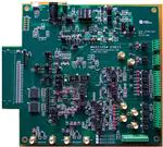


 工商网监
湘ICP备2023018690号
工商网监
湘ICP备2023018690号
