Enpirion® Power Datasheet
ER2120QI 2A Synchronous Buck
Regulator with Integrated MOSFETs
DS-1042
Datasheet
The Altera® Enpirion® ER2120QI is a synchronous buck
controller with internal MOSFETs packaged in a small
4mmx4mm QFN package. The ER2120QI can support a
continuous load of 2A and has a very wide input voltage
range. With the switching MOSFETs integrated into the IC,
the complete regulator footprint can be very small and provide
a much more efficient solution than a linear regulator.
The ER2120QI is capable of stand-alone operation or it can be
used in a master slave combination for multiple outputs that
are derived from the same input rail. Multiple slave channels
(up to six) can be synchronized. This method minimizes the
EMI and beat frequencies effect with multi-channel operation.
The switching PWM controller drives two internal N-Channel
MOSFETs in a synchronous-rectified buck converter topology.
The synchronous buck converter uses voltage-mode control
with fast transient response. The switching regulator provides
a maximum static regulation tolerance of 1% over line, load,
and temperature ranges. The output is user-adjustable by
means of external resistors down to 0.6V.
The output is monitored for undervoltage events. The
switching regulator also has overcurrent protection. Thermal
shutdown is integrated. The ER2120QI features a bi-directional
Enable pin that allows the part to pull the enable pin low
during fault detection.
POK delay for ER2120QI is 1ms typical (at 500kHz switching
frequency).
Features
•
•
•
•
•
•
•
•
•
•
•
•
•
•
•
•
Up to 2A Continuous Output Current
Integrated MOSFETs for Small Regulator Footprint
Adjustable Switching Frequency, 500kHz to 1.2MHz
Tight Output Voltage Regulation, 1% Over-temperature
Wide Input Voltage Range, 5V 10% or 5.5V to 14V
Wide Output Voltage Range, from 0.6V
Simple Single-Loop Voltage-Mode PWM Control Design
Input Voltage Feed-Forward for Constant Modulator Gain
Fast PWM Converter Transient Response
Lossless RDS(ON) High Side and Low Side Overcurrent
Protections
Undervoltage Detection
Integrated Thermal Shutdown Protection
Power-Good Indication
Adjustable Soft-Start
Start-Up with Pre-Bias Output
Pb-free (RoHS Compliant)
Applications
•
•
•
•
•
•
FPGA power
Point of Load Applications
Graphics Cards
ASIC Power Supplies
Embedded Processor and I/O Supplies
DSP Supplies
VIN
4.5V TO 5.5V
POWER GOOD
ENABLE
POK
EN
SYNC
M/S
AVIN
AVINO
SS
PVIN
+
VIN
5.5V TO 14V
POWER GOOD
ENABLE
BOOT
ER2120QI
SW
VOUT
+
PGND
FSW
POK
EN
AVINO
AVIN
SS
PVIN
BOOT
ER2120QI
SYNC
M/S
FSW
March 2014
+
PGND
FB
AGND
FIGURE 1. STAND-ALONE REGULATOR: VIN 5.5V TO 14V
101 Innovation Drive
San Jose, CA 95134
www.altera.com
VOUT
SW
FB
COMP
AGND
+
COMP
FIGURE 2. STAND-ALONE REGULATOR: VIN 4.5V TO 5.5V
© 2014 Altera Corporation. All rights reserved. ALTERA, ARRIA, CYCLONE, ENPIRION, HARDCOPY, MAX, MEGACORE, NIOS,
QUARTUS and STRATIX words and logos are trademarks of Altera Corporation and registered in the U.S. Patent and Trademark Office and in
other countries. All other words and logos identified as trademarks or service marks are the property of their respective holders as described at
www.altera.com/common/legal.html. Altera warrants performance of its semiconductor products to current specifications in accordance with
Altera's standard warranty, but reserves the right to make changes to any products and services at any time without notice. Altera assumes no
responsibility or liability arising out of the application or use of any information, product, or service described herein except as expressly agreed
to in writing by Altera. Altera customers are advised to obtain the latest version of device specifications before relying on any published
information and before placing orders for products or services.
ISO
9001:2008
Registered
Altera Corporation
Subscribe
09615
March 14, 2014
Rev A
�Page 2
Ordering Information
PART
NUMBER
(Note 1)
PART
MARKING
ER2120QI (Notes 1, 3)
2120
EVB-ER2120QI
Evaluation Board
TEMP. RANGE
(°C)
PACKAGE
(Pb-free)
-40 to +85
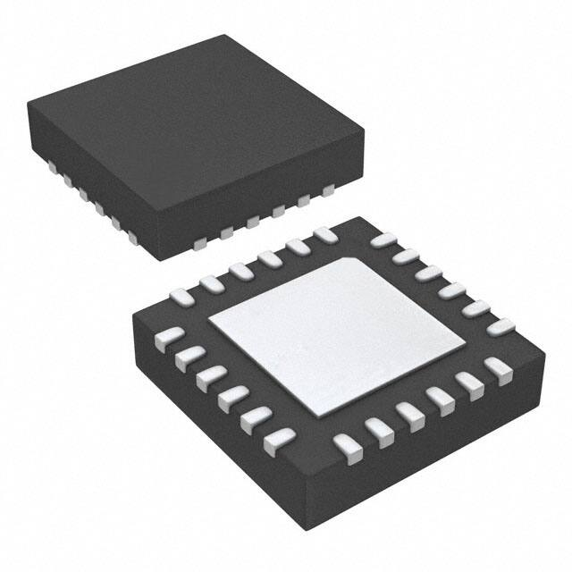
24 Ld 4x4 QFN
PKG. DWG. #
L24.4x4D
NOTES:
1. These Altera Enpirion Pb-free plastic packaged products employ special Pb-free material sets, molding compounds/die attach materials, and 100% matte tin
plate plus anneal (e3 termination finish, which is RoHS compliant and compatible with both SnPb and Pb-free soldering operations). Altera Enpirion Pb-free
products are MSL classified at Pb-free peak reflow temperatures that meet or exceed the Pb-free requirements of IPC/JEDEC J STD-020.
Pin Configuration
AVIN
AVINO
BOOT
PVIN
PVIN
PVIN
ER2120QI
(24 LD QFN)
TOP VIEW
24
23
22
21
20
19
POK
1
18 PVIN
AGND
2
17 SW
EN
3
SYNC
4
M/S
5
14 SW
FSW
6
13 PGND
16 SW
GND
25
7
8
9
10
11
12
COMP
FB
SS
PGND
PGND
PGND
15 SW
*See “Functional Pin Descriptions” beginning on page 13 for pin descriptions.
ER2120QI 2A Synchronous Buck Regulator with Integrated MOSFETs
09615
March 14, 2014
March 2014
Altera Corporation
Rev A
�Page 3
Typical Application Schematics
POWER GOOD
ENABLE
POK
PVIN
+
EN
VIN
5.5V TO 14V
SYNC
BOOT
M/S
AVIN
AVINO
ER2120QI
VOUT
SW
SS
+
PGND
FSW
FB
COMP
AGND
FIGURE 3. STAND-ALONE REGULATOR: VIN 5.5V TO 14V
VIN
4.5V TO 5.5V
POWER GOOD
ENABLE
POK
PVIN
EN
+
AVINO
BOOT
AVIN
SS
ER2120QI
VOUT
SW
+
SYNC
PGND
M/S
FSW
FB
COMP
AGND
FIGURE 4. STAND-ALONE REGULATOR: VIN 4.5V TO 5.5V
March 2014
09615
Altera Corporation
ER2120QI 2A Synchronous Buck Regulator with Integrated MOSFETs
March 14, 2014
Rev A
�Page 4
ER2120QI With Multiple Slaved Channels
VIN
MASTER
AVINO
M/S
SS
FSW
SYNC
RT
EN
PVIN
VOUT1
SW
+
GND
ER2120QI
ENABLE
M/S
PVIN
FSW
5k
RT
SYNC
EN
VOUT2
SW
+
GND
ER2120QI
SLAVE
M/S
PVIN
FSW
5k
RT
SYNC
EN
VOUTN
SW
+
GND
ER2120QI
SLAVE
ER2120QI 2A Synchronous Buck Regulator with Integrated MOSFETs
09615
March 14, 2014
March 2014
Altera Corporation
Rev A
�Page 5
Absolute Maximum Ratings
Thermal Information
PVIN. . . . . . . . . . . . . . . . . . . . . . . . . . . . . . . GND - 0.3V to +16.5V
AVIN. . . . . . . . . . . . . . . . . . . . . . . . . . . . . . . . GND - 0.3V to +6.0V
Absolute Boot Voltage, VBOOT . . . . . . . . . . . . . . . . . . . . . . . . +22.0V
Upper Driver Supply Voltage, VBOOT - VSW . . . . . . . . . . . . . . +6.0V
All other Pins . . . . . . . . . . . . . . . . . . . GND - 0.3V to AVIN + 0.3V
JA (°C/W) JC (°C/W)
Thermal Resistance
QFN Package (Notes 2, 2) . . . . . .
38
2
Maximum Junction Temperature (Plastic Package) . . . . . . . +150°C
Maximum Storage Temperature Range . . . . . . . . . -65°C to +150°C
Pb-free Reflow Profile. . . . . . . . . . . . . . . . . . . . . . . . . . . . . . . . . . —
Recommended Operating Conditions
Supply Voltage on PVIN . . . . . . . . . . . . . . . . . . . . . . . . 5.5V to 14V
Ambient Temperature Range . . . . . . . . . . . . . . . . . . -40°C to +85°C
Junction Temperature Range . . . . . . . . . . . . . . . . . -40°C to +125°C
CAUTION: Do not operate at or near the maximum ratings listed for extended periods of time. Exposure to such conditions may adversely impact
product reliability and result in failures not covered by warranty.
NOTES:
2. JA is measured in free air with the component mounted on a high effective thermal conductivity test board with “direct attach” features.
For JC, the “case temp” location is the center of the exposed metal pad on the package underside.
Electrical Specifications Refer to “Block Diagram” and “Typical Application Schematics”. Operating conditions unless otherwise
noted: VIN = 12V, or VAVIN = 5V ±10%, TA = -40°C to +85°C. Typical are at TA = +25°C. Boldface limits apply over the operating temperature
range,
-40°C to +85°C
PARAMETER
SYMBOL
TEST CONDITIONS
MIN
(Note 3)
MAX
(Note 3)
UNIT
S
5.5
(Note 4)
14
(Note 5)
V
4.5
5.5
V
TYP
VIN SUPPLY
PVIN Input Voltage Range
VIN
VIN tied to VAVIN
Input Operating Supply Current
IQ
VFB = 1.0V
IQ_SBY
EN tied to GND, VIN = 14V
AVIN Voltage
VAVINO
VIN > 5.6V
4.5
Maximum Output Current
IAVINO
VIN = 12V
50
Input Standby Supply Current
7
mA
1.25
2
mA
5.0
5.5
V
SERIES REGULATOR
AVIN Current Limit
VIN = 12V, AVIN shorted to PGND
mA
300
mA
POWER-ON RESET
Rising AVIN POR Threshold
4.2
4.4
4.49
V
Falling AVIN POR Threshold
3.85
4.0
4.10
V
ENABLE
Rising Enable Threshold Voltage
VEN_Rising
2.7
V
Falling Enable Threshold Voltage
VEN_Fall
2.3
V
Enable Sinking Current
IEN
500
µA
kHz
OSCILLATOR
PWM Frequency
fOSC
RT = 96k
400
500
600
RT = 40k
960
1200
1440
FSW pin tied to AVIN
kHz
Ramp Amplitude
VOSC
VIN = 14V
1.0
V
Ramp Amplitude
VOSC
VIN = 5V
0.470
V
Modulator Gain
VVIN/VOSC
By Design
8
-
Maximum Duty Cycle
DMAX
fOSC = 500kHz
88
%
Maximum Duty Cycle
DMAX
fOSC = 1.2MHz
76
%
March 2014
09615
kHz
800
Altera Corporation
ER2120QI 2A Synchronous Buck Regulator with Integrated MOSFETs
March 14, 2014
Rev A
�Page 6
Electrical Specifications Refer to “Block Diagram” and “Typical Application Schematics”. Operating conditions unless otherwise
noted: VIN = 12V, or VAVIN = 5V ±10%, TA = -40°C to +85°C. Typical are at TA = +25°C. Boldface limits apply over the operating temperature
range,
-40°C to +85°C
PARAMETER
SYMBOL
TEST CONDITIONS
MIN
(Note 3)
TYP
MAX
(Note 3)
UNIT
S
REFERENCE VOLTAGE
Reference Voltage
VREF
0.600
System Accuracy
-1.0
FB Pin Bias Current
±80
V
+1.0
%
±200
nA
µA
SOFT-START
Soft-Start Current
ISS
Enable Soft-Start Threshold
20
30
40
0.8
1.0
1.2
Enable Soft-Start Threshold
Hysteresis
12
Enable Soft-Start Voltage High
2.8
3.2
V
mV
3.8
V
ERROR AMPLIFIER
DC Gain
Gain-Bandwidth Product
GBWP
Maximum Output Voltage
Slew Rate
3.9
SR
88
dB
15
MHz
4.4
V
5
V/µs
INTERNAL MOSFETS
Upper MOSFET RDS(ON)
rDS_UPPER
VAVIN = 5V
180
m
Lower MOSFET RDS(ON)
rDS_LOWER
VAVIN = 5V
90
m
POK
POK Threshold
POK Rising Delay (Note 8)
VFB/VREF
tPOK_DELAY
POK Leakage Current
Rising Edge Hysteresis 1%
107
111
115
%
Falling Edge Hysteresis 1%
86
90
93
%
5
µA
0.5
mA
fOSC = 500kHz
1
VPOK = 5.5V
POK Low Voltage
VPOK
POK Sinking Current
IPOK
ms
0.10
V
PROTECTION
Positive Current Limit
Negative Current Limit
Undervoltage Level
IPOC_peak
INOC_peak
IOC from PVIN to SW (Notes 6, 7)
(TA = 0°C to +85°C)
2.1
3.5
4.5
A
IOC from PVIN to SW (Notes 6, 7)
(TA = -40°C to +0°C)
2.0
3.4
4.0
A
IOC from SW to PGND (Notes 6, 7)
(TA = 0°C to +85°C)
2.2
3.0
3.5
A
IOC from SW to PGND (Notes 6, 7)
(TA = -40°C to +85°C)
1.9
2.8
3.7
A
76
80
84
%
VFB/VREF
Thermal Shutdown Setpoint
TSD
150
°C
Thermal Recovery Setpoint
TSR
130
°C
ER2120QI 2A Synchronous Buck Regulator with Integrated MOSFETs
09615
March 14, 2014
March 2014
Altera Corporation
Rev A
�Page 7
Electrical Specifications Refer to “Block Diagram” and “Typical Application Schematics”. Operating conditions unless otherwise
noted: VIN = 12V, or VAVIN = 5V ±10%, TA = -40°C to +85°C. Typical are at TA = +25°C. Boldface limits apply over the operating temperature
range,
-40°C to +85°C
PARAMETER
SYMBOL
MIN
(Note 3)
TEST CONDITIONS
TYP
MAX
(Note 3)
UNIT
S
NOTES:
3. Parameters with MIN and/or MAX limits are 100% tested at +25°C, unless otherwise specified. Temperature limits established by
characterization and are not production tested.
4. Minimum VIN can operate below 5.5V as long as VAVIN is greater than 4.5V.
5. Maximum VIN can be higher than 14V voltage stress across the upper and lower do not exceed 15.5V in all conditions.
6. Circuit requires 150ns minimum on time to detect overcurrent condition.
7. Limits established by characterization and are not production tested.
8. POK Rising Delay is measured from the point where VOUT reaches regulation to the point where POK rises. It does not include the external
soft-start time. The POK Rising Delay specification is measured at 500kHz.
Typical Performance Curves
VIN = 12V, VOUT = 2.5V, IO = 2A, fSW = 500kHz, L = 4.7µH, CIN = 20µF,
100
100
90
90
80
80
EFFICIENCY (%)
EFFICIENCY (%)
COUT = 100µF + 22µF, TA = +25° C, unless otherwise noted.
VOUT = 2.5V
70
VOUT = 1.8V
VOUT = 3.3V
60
50
VOUT = 5.0V
70
VOUT = 3.3V
VOUT = 2.5V
60
VOUT = 1.8V
50
40
0.0
0.5
1.0
1.5
2.0
40
0.0
2.5
0.5
OUTPUT LOAD (A)
FIGURE 5. EFFICIENCY vs LOAD (VIN = 5V)
1.0
1.5
OUTPUT LOAD (A)
2.0
2.5
FIGURE 6. EFFICIENCY vs LOAD (VIN = 12V)
0.6026
1.206
14VIN
1.205
OUTPUT VOLTAGE (V)
OUTPUT VOLTAGE (V)
0.6025
0.6024
0.6023
14VIN
0.6022
0.6021
9VIN
0.6020
0.6019
1
OUTPUT LOAD (A)
09615
1.202
5VIN
1.200
2
FIGURE 7. VOUT REGULATION vs LOAD (VOUT = 0.6V, 500kHz)
March 2014
9VIN
1.203
1.201
5VIN
0
1.204
Altera Corporation
0
1
OUTPUT LOAD (A)
2
FIGURE 8. VOUT REGULATION vs LOAD (VOUT = 1.2V, 500kHz)
ER2120QI 2A Synchronous Buck Regulator with Integrated MOSFETs
March 14, 2014
Rev A
�Page 8
Typical Performance Curves
VIN = 12V, VOUT = 2.5V, IO = 2A, fSW = 500kHz, L = 4.7µH, CIN = 20µF,
COUT = 100µF + 22µF, TA = +25° C, unless otherwise noted. (Continued)
1.520
1.815
1.815
5VIN
1.814
5VIN
OUTPUT VOLTAGE (V)
OUTPUT VOLTAGE (V)
1.518
1.516
1.514
9VIN
14VIN
1.814
1.813
1.813
14VIN
1.812
9VIN
1.812
1.512
1.811
1.811
1.510
0
1
OUTPUT LOAD (A)
1.810
2
FIGURE 9. VOUT REGULATION vs LOAD (VOUT = 1.5V, 500kHz)
0
1
OUTPUT LOAD (A)
2
FIGURE 10. VOUT REGULATION vs LOAD (VOUT = 1.8V, 500kHz)
3.355
2.515
3.354
3.353
OUTPUT VOLTAGE (V)
OUTPUT VOLTAGE (V)
2.513
14VIN
2.511
2.509
5VIN
2.507
9VIN
3.352
5VIN
3.351
14VIN
3.350
3.349
3.348
3.347
9VIN
3.346
2.505
0
1
OUTPUT LOAD (A)
3.345
2
FIGURE 11. VOUT REGULATION vs LOAD (VOUT = 2.5V, 500kHz)
ER2120QI 2A Synchronous Buck Regulator with Integrated MOSFETs
09615
March 14, 2014
0
1
OUTPUT LOAD (A)
2
FIGURE 12. VOUT REGULATION vs LOAD (VOUT = 3.3V, 500kHz)
March 2014
Altera Corporation
Rev A
�Page 9
Typical Performance Curves
VIN = 12V, VOUT = 2.5V, IO = 2A, fSW = 500kHz, L = 4.7µH, CIN = 20µF,
COUT = 100µF + 22µF, TA = +25° C, unless otherwise noted. (Continued)
5.030
2.0
1.8
1.6
POWER DISSIPATION (W)
OUTPUT VOLTAGE (V)
5.028
7VIN
5.026
5.024
5.022
14VIN
0
14VIN
1.2
1.0
0.8
0.6
5VIN
0.4
9VIN
0.2
9VIN
5.020
1.4
1
OUTPUT LOAD (A)
0.0
0
2
FIGURE 13. VOUT REGULATION vs LOAD (VOUT = 5V, 500kHz)
1
OUTPUT LOAD (A)
2
FIGURE 14. POWER DISSIPATION vs LOAD (VOUT = 0.6V, 500kHz)
2.5
2.0
1.8
2.0
POWER DISSIPATION (W)
POWER DISSIPATION (W)
1.6
1.4
1.2
1.0
14VIN
0.8
0.6
5VIN
0.4
14VIN
0.5
5VIN
0
1
OUTPUT LOAD (A)
9VIN
0.0
2
March 2014
Altera Corporation
0
1
2
OUTPUT LOAD (A)
FIGURE 15. POWER DISSIPATION vs LOAD (VOUT = 1.2V, 500kHz)
09615
1.0
9VIN
0.2
0.0
1.5
FIGURE 16. POWER DISSIPATION vs LOAD (VOUT = 1.5V, 500kHz)
ER2120QI 2A Synchronous Buck Regulator with Integrated MOSFETs
March 14, 2014
Rev A
�Page 10
Typical Performance Curves
VIN = 12V, VOUT = 2.5V, IO = 2A, fSW = 500kHz, L = 4.7µH, CIN = 20µF,
2.5
2.5
2.0
2.0
1.5
POWER DISSIPATION (W)
POWER DISSIPATION (W)
COUT = 100µF + 22µF, TA = +25° C, unless otherwise noted. (Continued)
14VIN
1.0
0.5
0.0
5VIN
9VIN
0
1
OUTPUT LOAD (A)
14VIN
1.0
0.5
0.0
2
9VIN
0
1
2
FIGURE 18. POWER DISSIPATION vs LOAD (VOUT = 2.5V, 500kHz)
2.5
2.0
2.0
POWER DISSIPATION (W)
2.5
14VIN
1.5
5VIN
OUTPUT LOAD (A)
FIGURE 17. POWER DISSIPATION vs LOAD (VOUT = 1.8V, 500kHz)
POWER DISSIPATION (W)
1.5
1.0
0.5
14VIN
1.5
1.0
0.5
7VIN
5VIN
9VIN
0.0
0
1
9VIN
0.0
2
0
1
FIGURE 19. POWER DISSIPATION vs LOAD (VOUT = 3.3V, 500kHz)
FIGURE 20. POWER DISSIPATION vs LOAD (VOUT = 5V, 500kHz)
5.5
5.2
5.4
5.1
NO LOAD
5.3
5.0
5.2
AVIN (V)
AVIN
(V)
VCC (V)
2
OUTPUT LOAD (A)
OUTPUT LOAD (A)
4.9
4.8
5.1
5.0
4.9
100mA LOAD
4.8
4.7
4.7
4.6
4.5
4.6
0
50
100
150
IAVIN (mA)
200
250
300
3
4
5
6
7
8
9
10
VIN (V)
11
12
13
14 15
FIGURE 22. VAVIN REGULATION vs VIN
FIGURE 21. VAVIN LOAD REGULATION
ER2120QI 2A Synchronous Buck Regulator with Integrated MOSFETs
09615
4.5
March 14, 2014
March 2014
Altera Corporation
Rev A
�Page 11
Typical Performance Curves
VIN = 12V, VOUT = 2.5V, IO = 2A, fSW = 500kHz, L = 4.7µH, CIN = 20µF,
COUT = 100µF + 22µF, TA = +25° C, unless otherwise noted. (Continued)
SW1
5V/DIV
0.5µs
SW1
5V
5V/DIV
SW2
5V/DIV
VOUT1 RIPPLE
20mV/DIV
VOUT1 RIPPLE
20mV/DIV
IL1
0.5A/DIV
VOUT2 RIPPLE
20mV/DIV
SYNC1
2V/DIV
FIGURE 23. MASTER TO SLAVE OPERATION
FIGURE 24. MASTER OPERATION AT NO LOAD
SW1
10V/DIV
SW1
5V/DIV
VOUT1 RIPPLE
20mV/DIV
VOUT1 RIPPLE
20mV/DIV
IL1
1A/DIV
IL1
1A/DIV
SYNC1
5V/DIV
SYNC1
5V/DIV
FIGURE 25. MASTER OPERATION WITH FULL LOAD
March 2014
09615
Altera Corporation
FIGURE 26. MASTER OPERATION WITH NEGATIVE LOAD
ER2120QI 2A Synchronous Buck Regulator with Integrated MOSFETs
March 14, 2014
Rev A
�Page 12
Typical Performance Curves
VIN = 12V, VOUT = 2.5V, IO = 2A, fSW = 500kHz, L = 4.7µH, CIN = 20µF,
COUT = 100µF + 22µF, TA = +25° C, unless otherwise noted. (Continued)
EN1
5V/DIV
EN1
5V/DIV
VOUT1
0.5V/DIV
VOUT1
1V/DIV
2V PRE-BIASED
IL1
1A/DIV
IL1
2A/DIV
SS1
2V/DIV
FIGURE 27. SOFT-START AT NO LOAD
SS1
2V/DIV
FIGURE 28. START-UP WITH PRE-BIASED
SW1
10V/DIV
EN1
5V/DIV
VOUT1
1V/DIV
VOUT1
1V/DIV
IL1
1A/DIV
IL1
1A/DIV
SS1
2V/DIV
FIGURE 29. SOFT-START AT FULL LOAD
FIGURE 30. POSITIVE OUTPUT SHORT CIRCUIT
ER2120QI 2A Synchronous Buck Regulator with Integrated MOSFETs
09615
POK1
5V/DIV
March 14, 2014
March 2014
Altera Corporation
Rev A
�Page 13
Typical Performance Curves
VIN = 12V, VOUT = 2.5V, IO = 2A, fSW = 500kHz, L = 4.7µH, CIN = 20µF,
COUT = 100µF + 22µF, TA = +25° C, unless otherwise noted. (Continued)
SW1
10V/DIV
VOUT1
2V/DIV
SW1
10V/DIV
VOUT1
2V/DIV
IL1
2A/DIV
IL1
2A/DIV
SS1
2V/DIV
POK1
5V/DIV
FIGURE 31. POSITIVE OUTPUT SHORT CIRCUIT (HICCUP MODE)
SW1
10V/DIV
FIGURE 32. NEGATIVE OUTPUT SHORT CIRCUIT
VOUT1
1V/DIV
SW1
5V/DIV
IL1
1A/DIV
VOUT1 RIPPLE
50mV/DIV
IL1
2A/DIV
IOUT1
2A/DIV
POK1
5V/DIV
FIGURE 33. RECOVER FROM POSITIVE SHORT CIRCUIT
FIGURE 34. LOAD TRANSIENT
Functional Pin Descriptions
POK (Pin 1)
POK is an open drain output that pulls to low if the output goes out of regulation or a fault is detected. POK is equipped with a
fixed delay upon output power-up. The POK Rising Delay specification is measured at 500 kHz from the point where VOUT
reaches regulation to the point where POK rises. This delay is reversely proportional to the switching frequency.
AGND (Pin 2)
The AGND terminal of the ER2120QI provides the return path for the control and monitor portions of the IC.
EN (Pin 3)
The Enable pin is a bi-directional pin. If the voltage on this pin exceeds the enable threshold voltage, the part is enabled. If a fault is
detected, the EN pin is pulled low via internal circuitry for a duration of four soft-start periods. For automatic start-up, use 10k to
100k pull-up resistor connecting to AVIN.
March 2014
09615
Altera Corporation
ER2120QI 2A Synchronous Buck Regulator with Integrated MOSFETs
March 14, 2014
Rev A
�Page 14
SYNC (Pin 4)
SYNC is a bi-directional pin used to synchronize slave devices to the master device. As a master device, this pin outputs the clock
signal to which the slave devices synchronize. As a slave device, this pin is an input to receive the clock signal from the master
device.
If configured as a slave device, the ER2120QI is disabled if there is no clock signal from the master device on the SYNC pin.
Leave this pin unconnected if the IC is used in stand-alone operation.
M/S (Pin 5)
As a slave device, tie a 5k resistor between the M/S pin and ground.
As a master or a stand-alone device, tie the M/S pin directly to the AVIN pin. Do not short the M/S pin to GND.
FSW (Pin 6)
The FSW pin provides oscillator switching frequency adjustment. By placing a resistor (RT) from the FSW pin to GND, the
switching frequency can be programmed as desired between 500kHz and 1.2MHz as shown in Equation 1.
48000
R T k = -----------------------------f OSC kHz
(EQ. 1)
Tying the FSW pin to the AVIN pin forces the switching frequency to 800kHz.
Using resistors with values below 40k (1.2MHz) or with values higher than 97k (500kHz) may damage the ER2120QI.
COMP (Pin 7) and FB (Pin 8)
The switching regulator employs a single voltage control loop. The FB pin is the negative input to the voltage loop error amplifier.
The output voltage is set by an external resistor divider connected to FB. With a properly selected divider, the output voltage can
be set to any voltage between the power rail (reduced by converter losses) and the 0.6V reference. Loop compensation is achieved
by connecting an AC network across the COMP pin and the FB pin. The FB pin is also monitored for undervoltage events.
SS (Pin 9)
Connect a capacitor from the SS pin to ground. This capacitor, along with an internal 30µA current source, sets the soft-start
interval of the converter, tSS, as shown in Equation 2.
C SS F = 50 t SS S
(EQ. 2)
PGND (Pins 10-13)
The PGND pins are used as the ground connection of the power train.
SW (Pins 14-17)
The SW pins are the SW node connections to the inductor. These pins are connected to the source of the control MOSFET and the
drain of the synchronous MOSFET.
PVIN (Pins 18-21)
Connect the input rail to the PVIN pins. These pins are the input to the regulator as well as the source for the internal linear
regulator that supplies the bias for the IC.
It is recommended that the DC voltage applied to the PVIN pins does not exceed 14V. This recommendation allows for transient
spikes and voltage ringing to occur while not exceeding Absolute Maximum Ratings.
BOOT (Pin 22)
The BOOT pin provides ground-referenced bias voltage to the upper MOSFET driver. A bootstrap circuit is used to create a
voltage suitable to drive the internal N-channel MOSFET. The boot diode is included within the ER2120QI.
ER2120QI 2A Synchronous Buck Regulator with Integrated MOSFETs
09615
March 14, 2014
March 2014
Altera Corporation
Rev A
�Page 15
AVINO (Pin 23)
The AVINO pin is the output of the internal linear regulator that supplies the bias and gate voltage for the IC. A minimum 4.7µF
decoupling capacitor is recommended.
AVIN (Pin 24)
The AVIN pin supplies the bias voltage for the IC. This pin should be tied to the AVINO pin through an RC low pass filter. A 10
resistor and 0.1µF capacitor are recommended.
March 2014
09615
Altera Corporation
ER2120QI 2A Synchronous Buck Regulator with Integrated MOSFETs
March 14, 2014
Rev A
�Page 16
Block Diagram
AGND
EN
SYNC
M/S
FSW
PVIN
SERIES
REGULATOR
AVINO
CLOCK
AND
OSCILLATOR
GENERATOR
POR
MONITOR
AVIN
AVINO
BIAS
30A
VOLTAGE
MONITOR
FAULT MONITORING
0.6V
REFERENCE
FB
SS
COMP
POK
AVINO
OC
MONITOR
GATE
DRIVE
AND
ADAPTIVE
SHOOT THRU
PROTECTION
OC
MONITOR
PVIN (x4)
PGND (x4)
BOOT
SW (x4)
Rev A
March 14, 2014
09615
Altera Corporation
March 2014
ER2120QI 2A Synchronous Buck Regulator with Integrated MOSFETs
�Page 17
Functional Description
Initialization
The ER2120QI automatically initializes upon receipt of input power. The Power-On Reset (POR) function continuously monitors
the voltage on the AVIN pin. If the voltage on the EN pin exceeds its rising threshold, then the POR function initiates soft-start
operation after the bias voltage has exceeded the POR threshold.
Stand-alone Operation
The ER2120QI can be configured to function as a stand-alone single channel voltage mode synchronous buck PWM voltage
regulator. The “Typical Application Schematics” on page 3 show the two configurations for stand-alone operation.
The internal series linear regulator requires at least 5.5V to create the proper bias for the IC. If the input voltage is between 5.5V
and 15V, simply connect the PVIN pins to the input rail, and the series linear regulator creates the bias for the IC. The AVIN pin
should be tied to a capacitor for decoupling.
If the input voltage is 5V 10%, then tie the PVIN pins and the AVIN pin to the input rail. The ER2120QI uses the 5V rail as the
bias. A decoupling capacitor should be placed as close as possible to the AVIN pin.
Multi-Channel (Master/Slave) Operation
The ER2120QI can be configured to function in a multi-channel system. “ER2120QI With Multiple Slaved Channels” on page 4
shows a typical configuration for the multi-channel system.
In the multi-channel system, each ER2120QI IC regulates a separate rail while sharing the same input rail. By configuring the
devices in a master/slave configuration, the clocks of each IC can be synchronized.
There can only be one master IC in a multi-channel system. To configure an IC as the master, the M/S pin must be shorted to the
AVIN pin. The SYNC pins of all the ER2120QI controller ICs in the multi-channel system must be tied together. The frequency set
resistor value (RT) used on the master device must be used on every slave device. Each slave device must have a 5kresistor
connecting it from M/S pin to ground.
The master device and all slave devices can have their EN pins tied to an enable “bus.” Since the EN pin is bi-directional, it allows for
options on how each IC is tied to the enable bus. If the EN pin of any ER2120QI is tied directly to the enable bus, then that device is
capable of disabling all the other devices that have their EN pins tied directly to the enable bus. If the EN pin of an ER2120QI is tied to
the enable bus through a diode (anode tied to ER2120QI EN pin, cathode tied to enable bus), then the part does not disable other devices
on the enable bus if it disables itself for any reason.
If the master device is disabled via the EN pin, it continues to send the clock signal from the SYNC pin. This allows slave devices
to continue operating.
Fault Protection
The ER2120QI monitors the output of the regulator for overcurrent and undervoltage events. The ER2120QI also provides protection
from excessive junction temperatures.
OVERCURRENT PROTECTION
The overcurrent function protects the switching converter from a shorted output by monitoring the current flowing through both the
upper and lower MOSFETs.
Upon detection of any overcurrent condition, the upper MOSFET is immediately turned off and is not turned on again until the
next switching cycle. Upon detection of the initial overcurrent condition, the Overcurrent Fault Counter is set to 1, and the
Overcurrent Condition Flag is set from LOW to HIGH. If, on the subsequent cycle, another overcurrent condition is detected, the
OC Fault Counter is incremented. If there are eight sequential OC fault detections, the regulator is shut down under an Overcurrent
Fault Condition, and the EN pin is pulled LOW. An Overcurrent Fault Condition results, with the regulator attempting to restart in
hiccup mode. The delay between restarts is four soft-start periods. At the end of the fourth soft-start wait period, the fault counters
are reset, the EN pin is released, and soft-start is attempted again. If the overcurrent condition goes away prior to the OC Fault
Counter reaching a count of four, the Overcurrent Condition Flag is set back to LOW.
If the Overcurrent Condition Flag is HIGH, the Overcurrent Fault Counter is less than four, and an undervoltage event is detected,
the regulator shuts down immediately.
March 2014
09615
Altera Corporation
ER2120QI 2A Synchronous Buck Regulator with Integrated MOSFETs
March 14, 2014
Rev A
�Page 18
UNDERVOLTAGE PROTECTION
If the voltage detected on the FB pin falls 18% below the internal reference voltage, and if the overcurrent condition flag is LOW,
then the regulator is shut down immediately under an Undervoltage Fault Condition, and the EN pin is pulled LOW. An
Undervoltage Fault Condition results in the regulator attempting to restart in hiccup mode, with the delay between restarts being
four soft-start periods. At the end of the fourth soft-start wait period, the fault counters are reset, the EN pin is released, and softstart is attempted again.
THERMAL PROTECTION
If the ER2120QI IC junction temperature reaches a nominal temperature of +150°C, the regulator is disabled. The ER2120QI does
not re-enable the regulator until the junction temperature drops below +130°C.
SHOOT-THROUGH PROTECTION
A shoot-through condition occurs when both the upper and lower MOSFETs are turned on simultaneously, effectively shorting the
input voltage to ground. To protect from a shoot-through condition, the ER2120QI incorporates specialized circuitry, which
ensures that the complementary MOSFETs are not ON simultaneously.
Application Guidelines
Operating Frequency
The ER2120QI can operate at switching frequencies from 500kHz to 1.2MHz. A resistor tied from the FSW pin to ground is used
to program the switching frequency (Equation 3).
48000
R T k = -----------------------------f OSC kHz
(EQ. 3)
Output Voltage Selection
The output voltage of the regulator can be programmed via an external resistor divider that is used to scale the output voltage
relative to the internal reference voltage and feed it back to the inverting input of the error amplifier (see Figure 36).
The output voltage programming resistor, R4, depends on the value chosen for the feedback resistor and the desired output voltage
of the regulator. The value for the feedback resistor is typically between 1k and 10k.
R 1 0.6V
R 4 = ---------------------------------V OUT – 0.6V
(EQ. 4)
If the output voltage desired is 0.6V, then R4 is left unpopulated.
Output Capacitor Selection
An output capacitor is required to filter the inductor current and supply the load transient current. The filtering requirements are a function
of the switching frequency and the ripple current. The load transient requirements are a function of the slew rate (di/dt) and the magnitude
of the transient load current. These requirements are generally met with a mix of capacitors and careful layout.
High frequency capacitors initially supply the transient and slow the current load rate seen by the bulk capacitors. The bulk filter capacitor
values are generally determined by the ESR (Effective Series Resistance) and voltage rating requirements rather than actual capacitance
requirements.
High frequency decoupling capacitors should be placed as close to the power pins of the load as physically possible. Be careful not to add
inductance in the circuit board wiring that could cancel the usefulness of these low inductance components. Consult with the
manufacturer of the load on specific decoupling requirements.
The shape of the output voltage waveform during a load transient that represents the worst-case loading conditions ultimately determines
the number of output capacitors and their type. When this load transient is applied to the converter, most of the energy required by the
load is initially delivered from the output capacitors. This is due to the finite amount of time required for the inductor current to slew up to
the level of the output current required by the load. This phenomenon results in a temporary dip in the output voltage. At the very edge of
the transient, the Equivalent Series Inductance (ESL) of each capacitor induces a spike that adds on top of the existing voltage drop due to
the Equivalent Series Resistance (ESR).
ER2120QI 2A Synchronous Buck Regulator with Integrated MOSFETs
09615
March 14, 2014
March 2014
Altera Corporation
Rev A
�Page 19
DVHUMP
VOUT
DVESR
DVSAG
DVESL
IOUT
ITRAN
FIGURE 35. TYPICAL TRANSIENT RESPONSE
After the initial spike, attributable to the ESR and ESL of the capacitors, the output voltage experiences sag. This sag is a direct
consequence of the amount of capacitance on the output.
During removal of the same output load, the energy stored in the inductor is dumped into the output capacitors. This energy dumping
creates a temporary hump in the output voltage. This hump, as with the sag, can be attributed to the total amount of capacitance on the
output. Figure 35 shows a typical response to a load transient.
The amplitudes of the different types of voltage excursions can be approximated using Equation 5.
dI tran
V ESL = ESL --------------dt
V ESR = ESR I tran
2
L out I tran
V SAG = -------------------------------------------------C out V in – V out
2
L out I tran
V HUMP = -------------------------------C out V out
(EQ. 5)
where: Itran = Output Load Current Transient, and Cout = Total Output Capacitance.
In a typical converter design, the ESR of the output capacitor bank dominates the transient response. The ESR and ESL typically
are the major contributing factors in determining the output capacitance. The number of output capacitors can be determined by
using Equation 6, which relates the ESR and ESL of the capacitors to the transient load step and the voltage limit (DVo):
ESL dI tran
--------------------------------+ ESR I tran
dt
Number of Capacitors = ----------------------------------------------------------------------V o
(EQ. 6)
If DVSAG or DVHUMP is found to be too large for the output voltage limits, then the amount of capacitance may need to be
increased. In this situation, a trade-off between output inductance and output capacitance may be necessary.
The ESL of the capacitors, which is an important parameter in the previous equations, is not usually listed in databooks.
Practically, it can be approximated using Equation 7 if an Impedance vs Frequency curve is given for a specific capacitor:
1
ESL = ---------------------------------------2
C 2 f res
(EQ. 7)
where fres is the frequency at which the lowest impedance is achieved (resonant frequency).
The ESL of the capacitors becomes a concern when designing circuits that supply power to loads with high rates of change in the
current.
March 2014
09615
Altera Corporation
ER2120QI 2A Synchronous Buck Regulator with Integrated MOSFETs
March 14, 2014
Rev A
�Page 20
Output Inductor Selection
The output inductor is selected to meet the output voltage ripple requirements and to minimize the converter’s response time to the
load transient. The inductor value determines the converter’s ripple current, and the ripple voltage is a function of the ripple
current. The ripple voltage and current are approximated by using Equation 8:
DI =
VIN - VOUT
FSW x L
x
VOUT
DVOUT = DI x ESR
VIN
(EQ. 8)
Increasing the value of inductance reduces the ripple current and voltage. However, the large inductance values reduce the
converter response time to a load transient.
One of the parameters limiting converter response to a load transient is the time required to change the inductor current. Given
a sufficiently fast control loop design, the ER2120QI provides either 0% or 100% duty cycle in response to a load transient. The
response time is the time required to slew the inductor current from an initial current value to the transient current level. During
this interval, the difference between the inductor current and the transient current level must be supplied by the output
capacitor. Minimizing the response time can minimize the output capacitance required.
The response time to a transient is different for the application of load and the removal of load. Equation 9 gives the approximate
response time interval for application and removal of a transient load:
tRISE =
L x ITRAN
VIN - VOUT
tFALL =
L x ITRAN
VOUT
(EQ. 9)
where: ITRAN is the transient load current step, tRISE is the response time to the application of load, and tFALL is the response time to
the removal of load. The worst-case response time can be either at the application or removal of load. Be sure to check both of
these equations at the minimum and maximum output levels for the worst-case response time.
Input Capacitor Selection
Use a mix of input bypass capacitors to control the voltage overshoot across the MOSFETs. Use small ceramic capacitors for highfrequency decoupling, and bulk capacitors to supply the current needed each time the upper MOSFET turns on. Place the small
ceramic capacitors physically close to the MOSFETs and between the drain of the upper MOSFET and the source of the lower
MOSFET.
The important parameters for bulk input capacitance are the voltage rating and the RMS current rating. For reliable operation,
select bulk capacitors with voltage and current ratings above the maximum input voltage and largest RMS current required by the
circuit. Their voltage rating should be at least 1.25x greater than the maximum input voltage, while a voltage rating of 1.5x is a
conservative guideline. For most cases, the RMS current rating requirement for the input capacitor of a buck regulator is
approximately one-half the DC load current.
The maximum RMS current through the input capacitors can be closely approximated using Equation 10:
V OUT
V OUT 1 V IN – V OUT V OUT 2
2
--------------- I OUT
1 – --------------- + ------ ----------------------------- ----------------
V PVIN
V PVIN 12 L f OSC
V PVIN
MAX
(EQ. 10)
For a through-hole design, several electrolytic capacitors may be needed. For surface mount designs, solid tantalum capacitors can
be used, but caution must be exercised with regard to the capacitor surge current rating. These capacitors must be capable of
handling the surge current at power-up. Some capacitor series available from reputable manufacturers are surge current tested.
Feedback Compensation
Figure 36 highlights the voltage-mode control loop for a synchronous-rectified buck converter. The output voltage (VOUT) is
regulated to the reference voltage level. The error amplifier output (VE/A) is compared with the oscillator (OSC) triangular wave to
provide a pulse-width modulated (PWM) wave with an amplitude of VPVIN at the SW node. The PWM wave is smoothed by the
output filter (LO and CO).
The modulator transfer function is the small-signal transfer function of VOUT/VE/A . This function is dominated by a DC gain and
the output filter (LO and CO), with a double pole break frequency at FLC and a zero at FESR . The DC gain of the modulator is simply
the input voltage (VPVIN) divided by the
peak-to-peak oscillator voltage, DVOSC . The ER2120QI incorporates a feed-forward loop that accounts for changes in the input
voltage. This configuration maintains a constant modulator gain.
ER2120QI 2A Synchronous Buck Regulator with Integrated MOSFETs
09615
March 14, 2014
March 2014
Altera Corporation
Rev A
�Page 21
VIN
DRIVER
OSC
PWM
COMPARATOR
LO
-
VOSC
DRIVER
+
SW
VOUT
CO
ESR
(PARASITIC)
ZFB
VE/A
-
ZIN
+
REFERENCE
ERROR
AMP
DETAILED COMPENSATION COMPONENTS
ZFB
C1
C2
C3
R2
R3
R1
COMP
FB
+
ER2120QI
VOUT
ZIN
R4
REFERENCE
R
V OUT = 0.6 1 + ------1-
R 4
FIGURE 36. VOLTAGE-MODE BUCK CONVERTER COMPENSATION
DESIGN AND OUTPUT VOLTAGE SELECTION
Modulator Break Frequency Equations
1
f LC = ------------------------------------------2 x L O x C O
1
f ESR = -------------------------------------------2 x ESR x C O
(EQ. 11)
The compensation network consists of the error amplifier (internal to the ER2120QI) and the impedance networks, ZIN and ZFB.
The goal of the compensation network is to provide a closed loop transfer function with the highest 0dB crossing frequency (f0dB)
and adequate phase margin. Phase margin is the difference between the closed loop phase at f0dB and 180 degrees. Equation 12
relates the compensation network’s poles, zeros, and gain to the components (R1 , R2 , R3 , C1 , C2 and C3) in Figure 36. Use these
guidelines for locating the poles and zeros of the compensation network:
1. Pick Gain (R2/R1) for desired converter bandwidth.
2. Place first zero below filter’s double pole (~75% FLC).
3. Place second zero at filter’s double pole.
4. Place first pole at ESR Zero.
5. Place second pole at half the switching frequency.
6. Check gain against error amplifier’s open-loop gain.
7. Estimate phase margin; repeat if necessary.
March 2014
09615
Altera Corporation
ER2120QI 2A Synchronous Buck Regulator with Integrated MOSFETs
March 14, 2014
Rev A
�Page 22
Compensation Break Frequency Equations
1
f Z1 = -----------------------------------2 x R 2 x C 1
1
f P1 = -------------------------------------------------------- C 1 x C 2
2 x R 2 x ----------------------
C1 + C2
1
f Z2 = ------------------------------------------------------2 x R 1 + R 3 x C 3
1
f P2 = -----------------------------------2 x R 3 x C 3
(EQ. 12)
Figure 37 shows an asymptotic plot of the DC/DC converter gain vs frequency. The actual modulator gain has a high gain peak due
to the high Q factor of the output filter and is not shown in Figure 37. Using the guidelines provided should give a compensation
gain similar to the curve plotted. The open loop error amplifier gain bounds the compensation gain. Check the compensation gain
at FP2 with the capabilities of the error amplifier. The closed loop gain is constructed on the graph of Figure 37 by adding the
modulator gain (in dB) to the compensation gain (in dB). This is equivalent to multiplying the modulator transfer function to the
compensation transfer function and plotting the gain.
The compensation gain uses external impedance networks, ZFB and ZIN, to provide a stable, high bandwidth (BW) overall loop. A
stable control loop has a gain crossing with -20dB/decade slope and a phase margin greater than +45°. Include worst-case
component variations when determining phase margin.
100
fZ1 fZ2
fP1
fP2
80
OPEN LOOP
ERROR AMP GAIN
GAIN (dB)
60
40
20
20LOG
(R2/R1)
20LOG
(VIN/VOSC)
0
-40
-60
COMPENSATION
GAIN
CLOSED LOOP
GAIN
MODULATOR
GAIN
-20
fLC
10
100
1k
fESR
10k
100k
FREQUENCY (Hz)
1M
10M
FIGURE 37. ASYMPTOTIC BODE PLOT OF CONVERTER GAIN
Layout Considerations
Layout is very important in high frequency switching converter design. With power devices switching efficiently between 500kHz
and 1.2MHz, the resulting current transitions from one device to another cause voltage spikes across the interconnecting
impedances and parasitic circuit elements. These voltage spikes can degrade efficiency, radiate noise into the circuit, and lead to
device overvoltage stress. Careful component layout and printed circuit board design minimize these voltage spikes.
As an example, consider the turn-off transition of the control MOSFET. Prior to turn-off, the MOSFET is carrying the full load
current. During turn-off, current stops flowing in the MOSFET and is picked up by the lower MOSFET. Any parasitic inductance
in the switched current path generates a large voltage spike during the switching interval. Careful component selection, tight layout
of the critical components, and short, wide traces minimize the magnitude of voltage spikes.
There are two sets of critical components in the ER2120QI switching converter. The switching components are the most critical
because they switch large amounts of energy and therefore tend to generate large amounts of noise. Next are the small signal
components, which connect to sensitive nodes or supply critical bypass current and signal coupling.
A multi-layer printed circuit board is recommended. Figure 38 shows the connections of the critical components in the converter.
Note that capacitors CIN and COUT could each represent numerous physical capacitors. Dedicate one solid layer (usually a middle
layer of the PC board) for a ground plane, and make all critical component ground connections with vias to this layer. Dedicate
another solid layer as a power plane, and break this plane into smaller islands of common voltage levels. Keep the metal runs from
the SW terminals to the output inductor short. The power plane should support the input power and output power nodes. Use
copper-filled polygons on the top and bottom circuit layers for the phase nodes. Use the remaining printed circuit layers for small
signal wiring. The wiring traces from the GATE pins to the MOSFET gates should be kept short and wide enough to easily handle
the 1A of drive current.
ER2120QI 2A Synchronous Buck Regulator with Integrated MOSFETs
09615
March 14, 2014
March 2014
Altera Corporation
Rev A
�Page 23
In order to dissipate heat generated by the internal VTT LDO, the ground pad, pin 29, should be connected to the internal ground
plane through at least five vias. This allows heat to move away from the IC and also ties the pad to the ground plane through a low
impedance path.
The switching components should be placed close to the ER2120QI first. Minimize the length of connections between the input
capacitors, CIN, and the power switches by placing them nearby. Position both the ceramic and bulk input capacitors as close to the
upper MOSFET drain as possible. Position the output inductor and output capacitors between the upper and lower MOSFETs and
the load. Make the PGND and the output capacitors as short as possible.
The critical small signal components include any bypass capacitors, feedback components, and compensation components. Place
the PWM converter compensation components close to the FB and COMP pins. The feedback resistors should be located as close
as possible to the FB pin, with vias tied straight to the ground plane as required.
VIN
AVINO
5V
PVIN
CIN
CBP1
ER2120QI
L1
RBP
COMP
LOAD
PGND
CBP2
VOUT1
SW
AVIN
COUT1
C2
C1
R2
R1
FB
C3
R4
R3
GND PAD
KEY
ISLAND ON POWER PLANE LAYER
ISLAND ON CIRCUIT AND/OR POWER PLANE LAYER
VIA CONNECTION TO GROUND PLANE
FIGURE 38. PRINTED CIRCUIT BOARD POWER PLANES AND ISLANDS
Document Revision History
The table lists the revision history for this document.
Date
March 2014
March 2014
09615
Version
1.0
Altera Corporation
Changes
Initial release.
ER2120QI 2A Synchronous Buck Regulator with Integrated MOSFETs
March 14, 2014
Rev A
�Page 24
Package Outline Drawing
L24.4x4D
24 LEAD QUAD FLAT NO-LEAD PLASTIC PACKAGE
4.00
4X 2.5
A
20X 0.50
B
19
PIN 1
INDEX AREA
PIN #1 CORNER
(C 0 . 25)
24
1
18
4.00
2 . 50 ± 0 . 15
13
0.15
(4X)
12
7
0.10 M C A B
0 . 07
24X 0 . 23 +- 0
. 05 4
24X 0 . 4 ± 0 . 1
TOP VIEW
BOTTOM VIEW
SEE DETAIL "X"
0.10 C
C
0 . 90 ± 0 . 1
BASE PLANE
( 3 . 8 TYP )
SEATING PLANE
0.08 C
SIDE VIEW
(
2 . 50 )
( 20X 0 . 5 )
C
0 . 2 REF
5
( 24X 0 . 25 )
0 . 00 MIN.
0 . 05 MAX.
( 24X 0 . 6 )
DETAIL "X"
TYPICAL RECOMMENDED LAND PATTERN
NOTES:
1. Dimensions are in millimeters.
Dimensions in ( ) for Reference Only.
2. Dimensioning and tolerancing conform to AMSE Y14.5m-1994.
3. Unless otherwise specified, tolerance : Decimal ± 0.05
4. Dimension b applies to the metallized terminal and is measured
between 0.15mm and 0.30mm from the terminal tip.
5. Tiebar shown (if present) is a non-functional feature.
6. The configuration of the pin #1 identifier is optional, but must be
located within the zone indicated. The pin #1 identifier may be
either a mold or mark feature.
ER2120QI 2A Synchronous Buck Regulator with Integrated MOSFETs
09615
March 14, 2014
March 2014
Altera Corporation
Rev A
�


 工商网监
湘ICP备2023018690号
工商网监
湘ICP备2023018690号
