Automotive Grade
AUIRS211(7,8)S
SINGLE CHANNEL DRIVER
Features
Product Summary
Floating channel designed for bootstrap operation
Fully operational to +600 V
Tolerant to negative transient voltage - dV/dt immune
Gate drive supply range from 10 V to 20 V
Undervoltage lockout
CMOS Schmitt-triggered inputs with pull-down
(AUIRS2117) or pull-up (AUIRS2118)
Output in phase with input (AUIRS2117) or out of
Phase with input (AUIRS2118)
Leadfree, RoHS compliant
Automotive qualified*
Topology
Single High Side
≤ 600 V
VOFFSET
10 V – 20 V
VOUT
Io+ & I o- (typical)
290 mA & 600 mA
140 ns & 140 ns
tON & tOFF (typical)
Package Options
Typical Applications
Direct/Piezo injection
BLDC Motor Drive
MOSFET and IGBT drivers
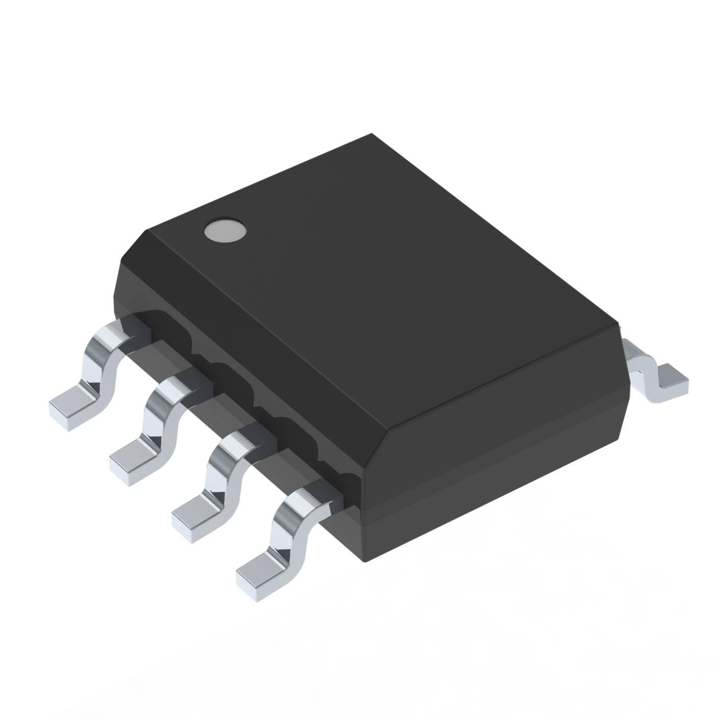
8-Lead SOIC
Typical Connection Diagram
Up to 600 V
Vcc
IN
Vcc
VB
IN
HO
COM
VS
TO
LOAD
AUIRS2117
Up to 600 V
Vcc
IN
(Refer to Lead Assignments for correct pin configuration). This/These
diagram(s) show electrical connections only. Please refer to our
Application Notes and Design Tips for proper circuit board layout.
1
www.irf.com
© 2014 International Rectifier
Vcc
VB
IN
HO
COM
VS
TO
LOAD
AUIRS2118
Submit Datasheet Feedback
July 15, 2014
�AUIRS211(7,8)S
Table of Contents
Page
Description
3
Qualification Information
4
Absolute Maximum Ratings
5
Recommended Operating Conditions
5
Static Electrical Characteristics
6
Dynamic Electrical Characteristics
6
Functional Block Diagram
7
Input/Output Pin Equivalent Circuit Diagram
8
Lead Definitions
9
Lead Assignments
9
Application Information and Additional Details
10-13
Parameter Temperature Trends
13-16
Package Details
17
Tape and Reel Details
18
Part Marking Information
19
Ordering Information
20
2
www.irf.com
© 2014 International Rectifier
Submit Datasheet Feedback
July 15, 2014
�AUIRS211(7,8)S
Description
The AUIRS2117S/AUIRS2118S are high voltage, high speed power MOSFET and IGBT drivers. Proprietary
HVIC and latch immune CMOS technologies enable ruggedized monolithic construction. The logic input is
compatible with standard CMOS outputs. The output drivers feature a high pulse current buffer stage. The
floating channel can be used to drive an N-channel power MOSFET or IGBT in the high- side or low-side
configuration which operates up to 600 V.
Qualification Information
†
Qualification Level
Moisture Sensitivity Level
Machine Model
Human Body Model
ESD
Charged Device Model
IC Latch-Up Test
RoHS Compliant
†
††
Automotive
(per AEC-Q100)
Comments: This family of ICs has passed an Automotive
qualification. IR’s Industrial and Consumer qualification
level is granted by extension of the higher Automotive
level.
††
MSL3 260°C
SOIC8N
(per IPC/JEDEC J-STD-020)
Class M2 (Pass +/-200V)
(per AEC-Q100-003)
Class H1B (Pass +/-1000V)
(per AEC-Q100-002)
Class C4 (Pass +/-1000V)
(per AEC-Q100-011)
Class II, Level A
(per AEC-Q100-004)
Yes
Qualification standards can be found at International Rectifier’s web site http://www.irf.com/
Higher MSL ratings may be available for the specific package types listed here. Please contact your
International Rectifier sales representative for further information.
3
www.irf.com
© 2014 International Rectifier
Submit Datasheet Feedback
July 15, 2014
�AUIRS211(7,8)S
Absolute Maximum Ratings
Absolute Maximum Ratings indicate sustained limits beyond which damage to the device may occur. All voltage
parameters are absolute voltages referenced to COM lead. Stresses beyond those listed under "
Absolute Maximum Ratings" may cause permanent damage to the device. These are stress ratings only; and
functional operation of the device at these or any other condition beyond those indicated in the “Recommended
Operating Conditions” is not implied. Exposure to absolute-maximum-rated conditions for extended periods may
affect device reliability. The thermal resistance and power dissipation ratings are measured under board
mounted and still air conditions. Ambient temperature (T A) is 25°C, unless otherwise specified.
Symbol
VB
Definition
Min.
Max.
-0.3
625
VB - 25
VS - 0.3
-0.3
-0.3
—
VB + 0.3
VB + 0.3
25
VCC + 0.3
50
V/ns
Package power dissipation @ TA ≤ 25°C
—
0.625
W
Thermal resistance, junction to ambient
—
200
°C/W
Junction temperature
Storage temperature
Lead temperature (soldering, 10 seconds)
—
-55
—
150
150
300
°C
High-side floating absolute voltage
VS
VHO
VCC
VIN
dVS/dt
PD
RthJA
TJ
TS
TL
High-side floating supply offset voltage
High-side floating output voltage
Logic supply voltage
Logic input voltage
Allowable offset supply voltage transient (Fig. 2)
Units
V
Recommended Operating Conditions
The input/output logic timing diagram is shown in Fig. 1. For proper operation the device should be used within
the recommended conditions. The VS offset rating is tested with all supplies biased at 15 V differential.
Symbol
VB
VS
VHO
VCC
VIN
TA
Definition
High-side floating supply absolute voltage
High-side floating supply offset voltage
High-side floating output voltage
Logic supply voltage
Logic input voltage
Ambient temperature
Min
VS +10
†
VS
10
0
-40
Max
VS +20
600
VB
20
VCC
125
Units
V
°C
† Logic operational for VS of -5 V to +600 V. Logic state held for VS of -5 V to – VBS.
(Please refer to the Design Tip DT97-3 for more details).
4
www.irf.com
© 2014 International Rectifier
Submit Datasheet Feedback
July 15, 2014
�AUIRS211(7,8)S
Static Electrical Characteristics
Unless otherwise noted, these specifications apply for an operating junction temperature range of -40°C ≤ Tj ≤
125°C with bias conditions of VBIAS (VCC, VBS) = 15 V. The VIL, VIH and IIN parameters are referenced to COM. The
VO and IO parameters are referenced to COM and are applicable to the respective output leads: HO.
Symbol
Definition
Min Typ Max Units
AUIRS2117
AUIRS2118
AUIRS2117
AUIRS2118
VIH
Logic “1” input voltage
9.5
—
—
VIL
Logic “0” input voltage
—
—
6.0
VOH
VOL
ILK
High level output voltage, VBIAS - VO
Low level output voltage, VO†
Offset supply leakage current
—
—
—
0.05
0.02
—
0.2
0.2
50
IQBS
Quiescent VBS supply current
—
50
240
IQCC
Quiescent VCC supply current
—
70
340
AUIRS2117
AUIRS2118
AUIRS2117
Logic “0” input bias current
AUIRS2118
VBS supply undervoltage positive going threshold
VBS supply undervoltage negative going threshold
VCC supply undervoltage positive going threshold
VCC supply undervoltage negative going threshold
—
20
40
—
—
5.0
7.6
7.2
7.6
7.2
8.6
8.2
8.6
8.2
9.6
9.2
9.6
9.2
Output high short circuit pulsed current
200 290
—
IIN+
IINVBSUV+
VBSUVVCCUV+
VCCUVIO+
Logic “1” input bias current
V
IO = 2 mA
VB = VS = 600 V
VIN = 0 V or VCC
µA
Output low short circuit pulsed current
VIN = VCC
VIN = 0 V
VIN = VCC
V
mA
IO-
Test Conditions
420 600
—
VO = 0 V,
VIN = Logic “1”
PW ≤ 10 µs
VO = 15 V,
VIN = Logic “0”
PW ≤ 10 µs
Dynamic Electrical Characteristics
Unless otherwise noted, these specifications apply for an operating junction temperature range of -40°C ≤ Tj ≤
125°C with bias conditions of VBIAS (VCC, VBS) = 15 V, CL = 1000 pF. The dynamic electrical characteristics are
measured using the test circuit shown in Fig. 3.
Symbol
Definition
Min
Typ
Max Units
ton
toff
tr
Turn-on propagation delay
Turn-off propagation delay
Turn-on rise time
—
—
—
140
140
75
225
225
130
tf
Turn-off fall time
—
25
65
ns
Test Conditions
VS = 0 V
VS = 600 V
Note: Please refer to figures in Parameter Temperature Trends section
5
www.irf.com
© 2014 International Rectifier
Submit Datasheet Feedback
July 15, 2014
�AUIRS211(7,8)S
Functional Block Diagram: (AUIRS2117)
AUIRS2117
VB
VCC
UV
DETECT
HV
LEVEL
SHIFTER
PULSE
FILTER
R
Q
R
S
HO
IN
PULSE
GENERATOR
VS
UV
DETECT
COM
Functional Block Diagram: (AUIRS2118)
AUIRS2118
6
www.irf.com
© 2014 International Rectifier
Submit Datasheet Feedback
July 15, 2014
�AUIRS211(7,8)S
Input/Output Pin Equivalent Circuit Diagrams: AUIRS2117S
VB
ESD
Diode
VCC
25V
HO
ESD
Diode
ESD
Diode
IN
RESD
RPD
VS
ESD
Diode
600V
VCC
COM
25V
COM
Input/Output Pin Equivalent Circuit Diagrams: AUIRS2118S
VB
ESD
Diode
VCC
25V
HO
RPU
ESD
Diode
ESD
Diode
IN
RESD
VS
ESD
Diode
600V
VCC
COM
25V
COM
7
www.irf.com
© 2014 International Rectifier
Submit Datasheet Feedback
July 15, 2014
�AUIRS211(7,8)S
Lead Definitions
PIN
Symbol
1
VCC
IN
IN
COM
NC
NC
VS
HO
VB
2
3
4
5
6
7
8
Description
Low-side and logic fixed supply
Logic input for gate driver output (HO), in phase with HO (AUIRS2117)
Logic input for gate driver output (HO), out of phase with HO (AUIRS2118)
Logic ground
No Connection
No Connection
High-side floating supply return
High-side gate drive output
High-side floating supply
Lead Assignments
1
VCC
VB
8
1
VCC
VB
8
2
IN
HO
7
2
IN
HO
7
3
COM
VS
6
3
COM
VS
6
5
4
4
5
8 Lead SOIC
8 Lead SOIC
AUIRS2117S
AUIRS2118S
Part Number
8
www.irf.com
© 2014 International Rectifier
Submit Datasheet Feedback
July 15, 2014
�AUIRS211(7,8)S
Application Information and Additional Details
HV = 10 V to 600 V
VCC = 15 V
IN
10 k F6
(AUIRS2118)
10 µF
0.1
µF
1
2
8
6
7
AUIRS2117
AUIRS2118
3
IN
(AUIRS2117)
+
100 µF
200
µH
0.1
µF
10 k
F6
HO
dVs
dt > 50 V/ns
OUTPUT 10 k F6
MONITOR
AUIRF820
HO
Figure 2: Floating Supply Voltage Transient
Test Circuit
Figure 1: Input/Output Timing Diagram
IN
VCC = 15 V
(AUIRS2118)
10 µF
IN
0.1
µF
1
2
8
6
7
10
µF
0.1
µF
CL
HO
VB
15 V
VS
(O V to 600 V)
10 µF
ton
Figure 3: Switching Time Test Circuit
www.irf.com
50%
50%
toff
tr
90%
HO
9
50%
IN
(AUIRS2117)
AUIRS2117
AUIRS2118
3
50%
© 2014 International Rectifier
10%
tf
90%
10%
Figure 4: Switching Time Waveform
Definition
Submit Datasheet Feedback
July 15, 2014
�AUIRS211(7,8)S
Tolerant to Negative VS Transients
A common problem in today’s high-power switching converters is the transient response of the switch node’s
voltage as the power switches transition on and off quickly while carrying a large current. A typical half bridge
circuit is shown in Figure 5; here we define the power switches and diodes of the inverter.
If the high-side switch (e.g., Q1 in Figures 6 and 7) switches off, while the current is flowing to a load, a current
commutation occurs from high-side switch (Q1) to the diode (D2) in parallel with the low-side switch of the
inverter. At the same instance, the voltage node VS swings from the positive DC bus voltage to the negative
DC bus voltage.
Figure 5: Half Bridge Circuit
Also when the current flows from the load back to the inverter (see Figures 8 and 9), and Q2 switches on, the
current commutation occurs from D1 to Q2. At the same instance, the voltage node V S swings from the positive
DC bus voltage to the negative DC bus voltage.
10
www.irf.com
© 2014 International Rectifier
Submit Datasheet Feedback
July 15, 2014
�AUIRS211(7,8)S
However, in a real inverter circuit, the VS voltage swing does not stop at the level of the negative DC bus,
rather it swings below the level of the negative DC bus. This undershoot voltage is called “negative VS
transient”.
The circuit shown in Figure 10 depicts a half bridge circuit with parasitic elements shown; Figures 11 and 12
show a simplified illustration of the commutation of the current between Q1 and D2. The parasitic inductances
in the power circuit from the die bonding to the PCB tracks are lumped together in LD and LS for each switch.
When the high-side switch is on, VS is below the DC+ voltage by the voltage drops associated with the power
switch and the parasitic elements of the circuit. When the high-side power switch turns off, the load current can
momentarily flow in the low-side freewheeling diode due to the inductive load connected to VS (the load is not
shown in these figures). This current flows from the DC- bus (which is connected to the COM pin of the HVIC)
to the load and a negative voltage between VS and the DC- Bus is induced (i.e., the COM pin of the HVIC is at
a higher potential than the VS pin).
In a typical power circuit, dV/dt is typically designed to be in the range of 1-5 V/ns. The negative VS transient
voltage can exceed this range during some events such as short circuit and over-current shutdown, when di/dt
is greater than in normal operation.
International Rectifier’s HVICs have been designed for the robustness required in many of today’s demanding
applications. An indication of the AUIRS2117(8)s’ robustness can be seen in Figure 13, where there is
represented the IRS2117(8)S Safe Operating Area at VBS=15V based on repetitive negative VS spikes. A
negative VS transient voltage falling in the grey area (outside SOA) may lead to IC permanent damage;
viceversa unwanted functional anomalies or permanent damage to the IC do not appear if negative Vs
transients fall inside SOA.
11
www.irf.com
© 2014 International Rectifier
Submit Datasheet Feedback
July 15, 2014
�AUIRS211(7,8)S
Figure 13: Negative VS transient SOA for AUIRS2117(8)S @ VBS=15V
Even though the AUIRS2117(8)S has shown the ability to handle these large negative VS transient conditions, it
is highly recommended that the circuit designer always limit the negative V S transients as much as possible by
careful PCB layout and component use.
12
www.irf.com
© 2014 International Rectifier
Submit Datasheet Feedback
July 15, 2014
�AUIRS211(7,8)S
Parameter Temperature Trends
Figures 14-28 provide information on the experimental performance of the AUIRS2117(8)S HVIC. The line
plotted in each figure is generated from actual lab data. A large number of individual samples were tested at
three temperatures (-40 ºC, 25 ºC, and 125 ºC) in order to generate the experimental curve.
The line consists of three data points (one data point at each of the tested temperatures) that have been
connected together to illustrate the understood trend. The individual data points on the Typ. curve were
determined by calculating the averaged experimental value of the parameter (for a given temperature).
Turn-off Propagation Delay (ns)
Turn-on Propagation Delay (ns)
220
190
160
M ax.
130 Typ.
M in.
100
-50
-25
0
25
50
75
100
220
190
160
M ax.
130 Typ.
M in.
100
125
-50
-25
0
o
25
50
75
100
125
o
Temperature ( C)
Temperature ( C)
Figure 5A.
Turn-On
Time
Figure 14. Turn-On
Time
vs. Temperature
Figure 15. Turn-Off Time vs. Temperature
vs. Temperature
50
Turn-Off fall Time (ns) -
Torn-On Rise Time (ns)
100
80
M ax.
60
Typ.
M in.
40
M ax.
30
Typ.
20
M in.
10
20
-50
-25
0
25
50
75
100
125
Temperature (oC)
Figure 16. Turn-On Rise Time vs. Temperature
13
40
www.irf.com
© 2014 International Rectifier
-50
-25
0
25
50
75
100
125
o
Temperature ( C)
Figure 17. Turn-Off Fall Time vs. Temperature
Submit Datasheet Feedback
July 15, 2014
�AUIRS211(7,8)S
0.25
Low Level Output Voltage(V)
High Level Output Voltage(V)
0.10
0.08
0.06
M ax.
Typ.
0.04
M in.
0.02
-50
-25
0
25
50
75
100
0.20
0.15
M ax.
0.10
0.05
Typ.
M in.
0.00
-50
125
-25
0
Figure 18. High Level Output Voltage vs. Temperature
75
100
125
Figure 19. Low Level Output Voltage vs. Temperature
50
100
V BS Supply Current (uA)
Offset Supply Leakage Current (uA)
50
Temperature ( C)
Temperature ( C)
35
M ax.
20
5
Typ.
-50
85
70
M ax.
55
Typ.
M in.
M in.
-10
40
-25
0
25
50
75
100
125
-50
-25
0
o
Temperature ( C)
100
125
20
Logic "1" Input Current (uA)
M ax.
100
Typ.
M in.
-50
-25
0
25
50
75
100
125
Temperature (oC)
Figure 22. VCC Supply Current vs. Temperature
14
75
Temperature ( C)
200
50
50
Figure 21. VBS Supply Current vs. Temperature
250
150
25
o
Figure 20. Offset Supply Leakage Current vs.
Temperature
VCC Supply Current (uA)
25
o
o
www.irf.com
© 2014 International Rectifier
18
16
14
M ax.
12
Typ.
10
M in.
-50
-25
0
25
50
75
100
125
o
Temperature ( C)
Figure 23. Logic “1” Input Current vs. Temperature
Submit Datasheet Feedback
July 15, 2014
�Logic "0" Input Current (uA).
-4.00
M ax.
Typ
-6.00
M in.
-8.00
-10.00
-12.00
-50
-25
0
25
50
75
100
125
Temperature (oC)
VCC Supply UV+ Going Threshold (V)
AUIRS211(7,8)S
8.3
8.1
Typ.
7.9
7.7
M in.
7.5
-50
-25
0
25
50
75
100
125
Temperature (oC)
8.4
Typ.
8.2
M in.
8.0
-50
-25
0
25
50
75
100
125
Temperature ( C)
9.0
8.8
8.6
M ax.
8.4
Typ.
8.2
M in.
8.0
-50
-25
0
25
50
75
100
125
o
Temperature ( C)
Figure 26. VCC Undervoltage Threshold (-) vs.
Temperature
VBS Supply UV- Going Threshold (V)
8.6
Figure 25. VCC Undervoltage Threshold (+) vs.
Temperature
VBS Supply UV+ Going Threshold (V)
VCC Supply UV- Going Threshold (V)
M ax
.
M ax.
8.8
o
Figure 24. Logic “0” (2118 “1”) Input Current vs.
Temperature
8.5
9.0
Figure 27. VBS Undervoltage Threshold (+) vs.
Temperature
8.5
M ax.
8.3
8.1
Typ.
7.9
7.7
M in.
7.5
-50
-25
0
25
50
75
100
125
Temperature (oC)
Figure 28. VBS Undervoltage Threshold (-) vs.
Temperature
15
www.irf.com
© 2014 International Rectifier
Submit Datasheet Feedback
July 15, 2014
�AUIRS211(7,8)S
Package Details: SOIC8
16
www.irf.com
© 2014 International Rectifier
Submit Datasheet Feedback
July 15, 2014
�AUIRS211(7,8)S
Tape and Reel Details: SOIC8
LOADED TAPE FEED DIRECTION
A
B
H
D
F
C
NOTE : CONTROLLING
DIMENSION IN MM
E
G
CARRIER TAPE DIMENSION FOR 8SOICN
Metric
Imperial
Code
Min
Max
Min
Max
A
7.90
8.10
0.311
0.318
B
3.90
4.10
0.153
0.161
C
11.70
12.30
0.46
0.484
D
5.45
5.55
0.214
0.218
E
6.30
6.50
0.248
0.255
F
5.10
5.30
0.200
0.208
G
1.50
n/a
0.059
n/a
H
1.50
1.60
0.059
0.062
F
D
C
B
A
E
G
H
REEL DIMENSIONS FOR 8SOICN
Metric
Code
Min
Max
A
329.60
330.25
B
20.95
21.45
C
12.80
13.20
D
1.95
2.45
E
98.00
102.00
F
n/a
18.40
G
14.50
17.10
H
12.40
14.40
17
www.irf.com
Imperial
Min
Max
12.976
13.001
0.824
0.844
0.503
0.519
0.767
0.096
3.858
4.015
n/a
0.724
0.570
0.673
0.488
0.566
© 2014 International Rectifier
Submit Datasheet Feedback
July 15, 2014
�AUIRS211(7,8)S
Part Marking Information
Part number
AS2117
Date code
AYWW ?
Pin 1
Identifier
IR logo
? XXXX
?
MARKING CODE
P
Lead Free Released
Assembly site code
Per SCOP 200-002
Non-Lead Free Released
Part number
AS2118
Date code
AYWW ?
Pin 1
Identifier
MARKING CODE
P
Lead Free Released
Non-Lead Free Released
18
www.irf.com
IR logo
? XXXX
?
© 2014 International Rectifier
Lot Code
(Prod mode –
4 digit SPN code)
Lot Code
(Prod mode –
4 digit SPN code)
Assembly site code
Per SCOP 200-002
Submit Datasheet Feedback
July 15, 2014
�AUIRS211(7,8)S
Ordering Information
Standard Pack
Base Part Number
AUIRS2117S
AUIRS2118S
19
www.irf.com
Package Type
Complete Part Number
Form
Quantity
Tube/Bulk
95
AUIRS2117S
Tape and Reel
2500
AUIRS2117STR
Tube/Bulk
95
AIRS2118S
Tape and Reel
2500
AUIRS2118STR
SOIC8
SOIC8
© 2014 International Rectifier
Submit Datasheet Feedback
July 15, 2014
�AUIRS211(7,8)S
IMPORTANT NOTICE
Unless specifically designated for the automotive market, International Rectifier Corporation and its subsidiaries
(IR) reserve the right to make corrections, modifications, enhancements, improvements, and other changes to
its products and services at any time and to discontinue any product or services without notice. Part numbers
designated with the “AU” prefix follow automotive industry and / or customer specific requirements with regards
to product discontinuance and process change notification. All products are sold subject to IR’s terms and
conditions of sale supplied at the time of order acknowledgment.
IR warrants performance of its hardware products to the specifications applicable at the time of sale in
accordance with IR’s standard warranty. Testing and other quality control techniques are used to the extent IR
deems necessary to support this warranty. Except where mandated by government requirements, testing of all
parameters of each product is not necessarily performed.
IR assumes no liability for applications assistance or customer product design. Customers are responsible for
their products and applications using IR components. To minimize the risks with customer products and
applications, customers should provide adequate design and operating safeguards.
Reproduction of IR information in IR data books or data sheets is permissible only if reproduction is without
alteration and is accompanied by all associated warranties, conditions, limitations, and notices. Reproduction
of this information with alterations is an unfair and deceptive business practice. IR is not responsible or liable
for such altered documentation. Information of third parties may be subject to additional restrictions.
Resale of IR products or serviced with statements different from or beyond the parameters stated by IR for that
product or service voids all express and any implied warranties for the associated IR product or service and is
an unfair and deceptive business practice. IR is not responsible or liable for any such statements.
IR products are not designed, intended, or authorized for use as components in systems intended for surgical
implant into the body, or in other applications intended to support or sustain life, or in any other application in
which the failure of the IR product could create a situation where personal injury or death may occur. Should
Buyer purchase or use IR products for any such unintended or unauthorized application, Buyer shall indemnify
and hold International Rectifier and its officers, employees, subsidiaries, affiliates, and distributors harmless
against all claims, costs, damages, and expenses, and reasonable attorney fees arising out of, directly or
indirectly, any claim of personal injury or death associated with such unintended or unauthorized use, even if
such claim alleges that IR was negligent regarding the design or manufacture of the product.
IR products are neither designed nor intended for use in military/aerospace applications or environments unless
the IR products are specifically designated by IR as military-grade or “enhanced plastic.” Only products
designated by IR as military-grade meet military specifications. Buyers acknowledge and agree that any such
use of IR products which IR has not designated as military-grade is solely at the Buyer’s risk, and that they are
solely responsible for compliance with all legal and regulatory requirements in connection with such use.
IR products are neither designed nor intended for use in automotive applications or environments unless the
specific IR products are designated by IR as compliant with ISO/TS 16949 requirements and bear a part
number including the designation “AU”. Buyers acknowledge and agree that, if they use any non-designated
products in automotive applications, IR will not be responsible for any failure to meet such requirements.
For technical support, please contact IR’s Technical Assistance Center
http://www.irf.com/technical-info/
WORLD HEADQUARTERS:
101 N. Sepulveda Blvd., El Segundo, California 90245
Tel: (310) 252-7105
20
www.irf.com
© 2014 International Rectifier
Submit Datasheet Feedback
July 15, 2014
�AUIRS211(7,8)S
Revision History
Date
Comment
MM/DD/YY
6/17/08
9/26/08
02/10/09
Original document
Converted the datasheet to the new format.
Reviewed and added missing graphs, inserted input/output Pin Equivalent Diagrams
Typ application section and other minor changes
Reviewed electrical spec, updated test temperature, qual info, package info I/O equivalent
diagram page.
Reviewed electrical spec, updated test temperature and plots, add –VS note.
Updated figure numbers and page number table
Changed Ton/off typ to 150ns; Matched Toff delay to be same as Ton delay
Added ESD passing voltage; still need LU test result.
Added latch up test classification
Updated Voh and Vol graphs; changed Ton/off typ. 150 to 140, max. 200 to 225; Vol 0.1 to
0.2; Tf 35 to 25; IN- 5 to 1
Updated typ application section, Max Vs oper cond changed from 200V to 600V.
Removed parameter vs. voltage graphs.
Added Important Notice disclaimer, updated typ ton/off to 140nS & Max. to 225 nS, removed
SOIC8 from PD description, updated VOL max to 0.2A, tf typical to 25nS.
Corrected typical applications on front page from “BLCD” to “BLDC”; updated disclaimer
under Abs. Max. Rating.
Vin low limit corrected from 0.3 to -0.3V in Abs.Max.Ratings;
Removed note II from AEC-Q100 (Page 3);
Updated World Headquarters address (Page 20)
08/03/09
08/11/09
08/12/09
8/14/09
9/23/09
9/23/09
10/16/09
10/27/09
11/5/09
12/8/09
2/2/2010
07/15/2014
21
www.irf.com
© 2014 International Rectifier
Submit Datasheet Feedback
July 15, 2014
�


 工商网监
湘ICP备2023018690号
工商网监
湘ICP备2023018690号
