AN_201604_PL52_018
45 W adapter demo board
Using the new 800 V CoolMOS™ P7 and ICE2QS03G quasi-resonant PWM
controller
Authors:
Jared Huntington
Stefan Preimel
Scope and purpose
The demo board described in this application note provides a test platform for the new 800 V CoolMOS™ P7
series of high voltage MOSFETs. The adapter uses ICE2QS03G, a second generation current mode control quasiresonant flyback controller and an IPA80R450P7 800 V CoolMOS™ P7 series power MOSFET. This application
note is intended for those that have experience with flyback converter designs and will not go in depth about the
overall design process for flyback converters, but will cover specific design aspects for this controller and 800 V
CoolMOS™ P7 in charger and adapter applications. It will also look at the overall benefits that the 800 V
CoolMOS™ P7 presents for switch mode power supplies. For a detailed introduction on flyback converter design
please read Design guide for QR Flyback converter [1].
Intended audience
Power supply design engineers
Table of contents
1
Description.........................................................................................................................................2
2
Quasi-resonant flyback overview.......................................................................................................3
3
ICE2QS03G functional overview.........................................................................................................4
4
4.1
800 V CoolMOS P7 overview .............................................................................................................5
FullPAK vs. DPAK thermal performance .................................................................................................7
5
5.1
5.2
Design considerations........................................................................................................................9
800 V MOSFET ..........................................................................................................................................9
UVLO circuit ...........................................................................................................................................10
6
6.1
6.2
6.3
6.4
6.5
6.6
6.7
Demo board overview ......................................................................................................................12
Demo board pictures.............................................................................................................................12
Demo board specifications ...................................................................................................................12
Demo board features ............................................................................................................................13
Schematic ..............................................................................................................................................14
BOM with Infineon components in bold...............................................................................................15
PCB layout .............................................................................................................................................16
Transformer construction.....................................................................................................................17
7
7.1
7.2
7.3
7.4
Measurements .................................................................................................................................19
Test measurements under different line and load conditions ............................................................19
Normal operation..................................................................................................................................20
Surge testing..........................................................................................................................................22
Thermal performance under typical operating conditions.................................................................23
8
Conclusion .......................................................................................................................................26
9
References .......................................................................................................................................27
™
Application Note
www.infineon.com/p7
Please read the Important Notice and Warnings at the end of this document
Revision 1.0
2016-06-27
�45 W adapter demo board
Using the new 800 V CoolMOS™ P7 and ICE2QS03G quasi-resonant PWM controller
Description
1
Description
This 45 W adapter demo board is intended to be a form, fit and function test platform for charger and adapter
applications to show the operation of the 800 V CoolMOS™ P7 as well as the overall controller design. The
demo board is designed around a quasi-resonant flyback topology for improved switching losses which allows
higher power density designs and lower radiated and conducted emissions. A 45 W universal input isolated
flyback demo board with a 19 V output based on the ICE2QS03G controller and the P7 MOSFET is described in
this application note and test results are presented.
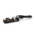
Figure 1
45 W flyback demo board
Application Note
2
Revision 1.0
2016-06-27
�45 W adapter demo board
Using the new 800 V CoolMOS™ P7 and ICE2QS03G quasi-resonant PWM controller
Quasi-resonant flyback overview
2
Quasi-resonant flyback overview
The QR flyback offers improved efficiency and EMI performance over the traditional fixed frequency flyback
converter by reducing switching losses. This is accomplished by controlling the turn on time of the primary
MOSFET (Qpri in Figure 3). In a flyback operating in discontinuous conduction mode (DCM) the energy is first
stored in the primary side when the primary MOSFET Qpri is turned on allowing the primary current to ramp up.
The primary MOSFET (Qpri) turns off and then the energy stored in the transformer transfers into the secondary
side capacitor. The energy that is left in the primary inductance (Lpri) after transferring the energy to the
secondary then resonates with the combined output capacitance of the MOSFET(CDS_parasitic) consisting of the
MOSFET output capacitance (COSS), stray drain source capacitance from the transformer and layout, and any
additional added external drain source capacitance on this node. In a fixed frequency flyback the switch turn on
happens regardless of the VDS voltage from the MOSFET drain to source. If switching occurs at a higher VDS (Figure
2) this corresponds to more switching losses (EOSS losses). The QR flyback waits to turn on Qpri until the VDS
voltage reaches the minimum possible voltage shown in Figure 2 and then turns on the MOSFET.
_
= 0.5
Since the turn on switching losses are a function of V2 (as shown above), this drastically reduces the overall
system switching losses. This has the added benefit of lowering the amount of switched energy which helps
reduce switching noise from the converter, resulting in lower radiated and conducted emissions.
800 V CoolMOS™ P7 technology helps improve performance in a QR flyback by allowing an increase in the
reflected voltage. This increase in reflected voltage increases the energy stored in the magnetizing inductance
during the DCM period which allows switching at an even lower VDS voltage allowing even lower switching losses.
The 800 V CoolMOS™ P7 also has a lower gate charge (QG) and output capacitance (COSS) which help to further
reduce the switching losses of the MOSFET.
MOSFET Turn ON
MOSFET Turn ON
Figure 2
Fixed frequency flyback primary MOSFET drain source waveform (left) vs. a quasi-resonant flyback
primary MOSFET drain source waveform (right).
Figure 3
Simplified flyback schematic
Application Note
3
Revision 1.0
2016-06-27
�45 W adapter demo board
Using the new 800 V CoolMOS™ P7 and ICE2QS03G quasi-resonant PWM controller
ICE2QS03G functional overview
3
ICE2QS03G functional overview
The PWM controller ICE2QS03G is a second generation quasi-resonant flyback controller IC developed by
Infineon Technologies. The typical applications include TV-sets, DVD-players, set-top boxes, netbook adapters,
home audio, and printer applications. This controller implements switching at the lowest ringing voltage and
also includes pulse skipping at light loads for maximum efficiency across a wide range of loads.
Figure 4
ICE2QS03G pinout
Table 1
ICE2QS03G pin description
Pin
Name
Description
1
Zero Crossing (ZC)
Detects the minimum trough (valley) voltage for turn on for the primary
switch turn on time
2
Feedback (FB)
Voltage feedback for output regulation
3
Current Sense (CS)
Primary side current sense for short circuit protection and current
mode control
4
Gate drive output (GATE)
MOSFET gate driver pin
5
High Voltage (HV)
Connects to the bus voltage for the initial startup through the high
voltage startup cell
6
No Connect (NC)
No connection
7
Power supply (VCC)
Positive IC for the power supply
8
Ground (GND)
Controller ground
Application Note
4
Revision 1.0
2016-06-27
�45 W adapter demo board
Using the new 800 V CoolMOS™ P7 and ICE2QS03G quasi-resonant PWM controller
800 V CoolMOS™ P7 overview
™
4
800 V CoolMOS P7 overview
The 800 V P7 family of MOSFETs provides several advantages for flyback converters. The 800 V CoolMOS™ P7
offers a cost reduction for the same RDS(on) device when compared to the C3 series with an improvement in
performance. The switching losses of the devices are lowered due to reduced device parasitic elements such as
COSS and QG. These improvements diminish as the MOSFET drain source voltage during turn on gets lower. The
greatest reduction in switching losses is seen at higher drain source switching voltages and at low output powers
due to the improved output parasitic elements (COSS). The reduction in overall switching losses of the device
allows moving to a higher RDS(ON) to further reduce the BOM cost or allow increasing the power density of the
power supply design.
PSpice models of the P7 800 V MOSFETs are provided on the Infineon website. These models have been fitted
with measurements of the devices and provide a high level of accuracy. Below, Figure 5 shows the difference
between the Infineon 45 W adapter measured waveforms and the simulated waveforms. These models can be
used to better understand the loss mechanisms that are responsible for power dissipation in the primary
MOSFET of the flyback converter and help optimize designs.
Figure 5
Simulated switching vs. measured switching at 230 VAC operation.
Application Note
5
Revision 1.0
2016-06-27
�45 W adapter demo board
Using the new 800 V CoolMOS™ P7 and ICE2QS03G quasi-resonant PWM controller
800 V CoolMOS™ P7 overview
Using the P7 PSpice models for the 45 W adapter, we can look at the losses occurring in the MOSFET of the 45 W
adapter flyback converter. The figure below shows the breakdown of the MOSFET turn on losses, turn off
losses, and conduction losses. As shown in Figure 6, the switching losses of the MOSFET are a more significant
loss contributor at high line. The figure below shows the breakdown of MOSFET turn on losses, turn off losses,
and conduction losses at high line. At low line the conduction losses (RDS(ON)) dominate and the improvement in
COSS does not make such a large improvement. The IPA80R1K4P7 MOSFET offers lower switching losses which
give a total power savings of 15.6 mW at high line over the original C3 series SPA06N80C3 - with a large
reduction in cost.
160
140
Power Loss (mW)
120
100
80
60
Gate
40
Turn-Off
Conduction
20
Turn-On
0
SPA11N80C3 High line
IPA80R1K4P7 High line
MOSFET and Line Voltage
Figure 6
Switching losses of SPA11N80C3 vs. IPA80R450P7 at 230 VAC input
0,1
0,0
-0,1
5
10
15
20
25
30
35
40
45
Efficiency [%]
-0,2
-0,3
SPA11N80C3
Comp. 1
Comp. 2
IPA80R450P7
-0,4
-0,5
-0,6
-0,7
-0,8
-0,9
Figure 7
Pout [W]
IPA80R450P7 set as the efficiency reference measured in the 45 W adapter in comparison with the
SPA11N80C3 and a competitor’s equivalent component at 230 VAC.
Application Note
6
Revision 1.0
2016-06-27
�45 W adapter demo board
Using the new 800 V CoolMOS™ P7 and ICE2QS03G quasi-resonant PWM controller
800 V CoolMOS™ P7 overview
It can be seen in Figure 7 that the IPA80R450P7 has improved performance when compared to the C3 series of
MOSFETs and two of our competitors latest generation of MOSFETs. At light loads the switching losses are
dominant and it can be seen that the P7 switching performance is much better.
*Simulations and modeling done by Stefano De Filippis
4.1
FullPAK vs. DPAK thermal performance
The DPAK MOSFET package is ideal for low cost applications such as charger and adapters. The thermal
performance is slightly lower than the TO-220 FullPAK (TO-220FP), but it has a lower package cost allowing for
overall BOM savings. The DPAK also has a smaller form factor allowing for higher power density designs and the
SMD placement to be used. In the Infineon 45 W adapter allows a TO-220FP or a DPAK footprint. The two
packages were tested on the same board under full load (45 W) at 120 VAC and 230 VAC in a 25°C ambient to show
the thermal performance difference between the two packages.
Table 2
FullPAK vs. DPAK thermal performance (25°C ambient)
Test conditions
IPD80R450P7
IPA80R450P7
DPAK case temp. rise(°C) FullPAK case temp. rise(°C)
DPAK temp. increase from
FullPAK(°C)
45 W, 120 VAC, 60 Hz,
56.8°C
27.7°C
29.1°C
45 W, 230 VAC, 50 Hz
51.8°C
25.9°C
25.9°C
In the infrared thermal images below, the primary MOSFET Q1 is called out in the black boxes. It can be seen that
the temperature of the DPAK is 29.1°C higher than the FullPAK at 120 VAC. Most of this temperature difference is
due to the fact that the MOSFET (when placed on the bottom side of the printed circuit board) receives some
heating from the surrounding components (the snubber and transformer). Figure 10 shows the DPAK footprint
temperature rise while the power supply is operating using the FullPAK. This increases the package temperature
in addition to the difference in package thermal resistance leading to a higher temperature. The hottest
components on the board are the snubber network resistors, R22 and R23, shown below in Figure 8. Table 3
takes the DPAK thermal rise and removes the PCB temperature rise of the footprint with the FullPAK in place.
The DPAK temperature is then overcorrected due to some heating of the PCB from the FullPAK causing a higher
footprint temperature.
Table 3
FullPAK vs. DPAK thermal performance normalized for PCB rise (25 °C ambient)
IPD80R450P7
DPAK case
temp. rise(°C)
IPD80R450P7
DPAK footprint
temp. rise(°C)
DPAK case temp.
increase from PCB
temp. (°C)
DPAK temp.
increase from
FullPAK (°C)
45 W, 120 VAC, 60 Hz
56.8°C
30.1°C
26.7°C
-1.0°C
45 W, 230 VAC, 50 Hz
51.8°C
29.5°C
22.3°C
-3.6°C
Test conditions
A 50°C ambient would push the total DPAK temperature up to 106.8°C in this specific design. Depending on the
required ambient operating conditions the DPAK package in this application would require a larger copper area
or lower output power in order to have enough thermal margins under worst case conditions.
The DPAK package can be used to give space, cost, and assembly savings, but the additional heating of
surrounding components and reduced thermal performance needs to be considered when switching from a
FullPAK to a DPAK package.
Application Note
7
Revision 1.0
2016-06-27
�45 W adapter demo board
Using the new 800 V CoolMOS™ P7 and ICE2QS03G quasi-resonant PWM controller
800 V CoolMOS™ P7 overview
Q1
Figure 8
45 W adapter bottom using DPAK at 45 W load and 120 VAC. Q1 shown above in the black box is the
flyback converter primary MOSFET. Note the MOSFET Q1 is receiving some heating from the
surrounding components which contributes to the higher DPAK temperature.
Q1
Figure 9
45 W adapter top using FullPAK at 45 W load and 120 VAC. Q1 shown above in the black box is the
flyback converter primary MOSFET.
Q1
Figure 10
45 W adapter bottom using FullPAK at 45 W load and 100 VAC. The DPAK footprint is shown and the
local PCB temperature rise can be seen which further increases the DPAK temperature.
Application Note
8
Revision 1.0
2016-06-27
�45 W adapter demo board
Using the new 800 V CoolMOS™ P7 and ICE2QS03G quasi-resonant PWM controller
Design considerations
5
Design considerations
5.1
800 V MOSFET
The 800 V CoolMOS™ P7 provides several benefits for charger and adapter applications. An 800 V breakdown
voltage allows a higher combination of bus voltage, reflected voltage, and snubber voltage than can be achieved
with a 600 V or 650 V device. By allowing a higher reflected voltage and snubber voltage the system power losses
can be reduced while maintaining higher breakdown voltage margins.
Figure 11
MOSFET VDS during turn off in the Infineon 45 W adapter
In this specific design the reflected voltage was increased from the Infineon 35 W adaptor which used a 600 V
device. This section will compare the Infineon 35 W adapter design using a 600 V MOSFET with the Infineon 45 W
adapter using an 800 V MOSFET to show the difference in performance between the two designs.
The reflected voltage determines the trough (valley) voltage during DCM ringing where the switch turns on in the
QR flyback converter. By allowing a higher reflected voltage there is a resulting lower trough in the ringing
waveform. This allows the converter to switch at a lower VDS voltage and reduce the system's switching losses
especially at high line (265 VAC) operation.
_
= 0.5
Table 4
=
_
+
Parameter
Symbol
600 V design
800 V P7 design
Transformer primary turns
NP
66 turns
87 turns
Transformer secondary turns
NS
11 turns
8 turns
Output voltage
Voutput
19 V
19 V
Diode forward voltage
Vforward
0.55 V
0.4 V
Transformer reflected voltage
Vreflected
117 V
211 V
Application Note
9
Revision 1.0
2016-06-27
�45 W adapter demo board
Using the new 800 V CoolMOS™ P7 and ICE2QS03G quasi-resonant PWM controller
Design considerations
The primary side resistor, capacitor, and diode (RCD) snubber network resistor power dissipation was reduced
allowing the snubber voltage to reach a higher level and lowering the amount of energy that is dissipated in the
snubber resistor. This especially comes into effect at very light load operation.
=
Table 5
+2
=
−
Parameter
Symbol
600 V design
800 V P7 design
Leakage inductance
Lleakage
25 µH
25 µH
Peak primary current under load at high line
Ipri
0.43 A
0.48 A
Snubber resistor
Rsnubber
54 kΩ
300 kΩ
Switching period
Ts
28.6 µs
28.6 µs
Snubber voltage
Vsnubber
40.1 V
127 V
Increasing the reflected voltage and lowering the amount of energy that is dissipated in the snubber lowers the
overall system losses and would not be possible with a 600 V MOSFET as shown in Table 5. Even with increasing
the reflected voltage by 94 V and increasing the snubber voltage by 30.4 V we still have an increase in margin
from the MOSFET breakdown voltage. In this new design the margin has increased from 12% to 15% even with
increasing the VDS voltages. This allows for the design of flyback converters running from higher input bus
voltages or those that need margin for abnormal conditions such as surge.
Table 6
Parameter
Symbol
600 V design
800 V P7 design
Primary bus voltage @265 VAC
Vbus
373 V
373 V
Reflected voltage
Vreflected
117 V
211 V
Snubber voltage
Vsnubber
40.1 V
70.5 V
Drain source voltage maximum
VDS_max
526 V
622 V
Margin from breakdown voltage
VDS_margin
12 %
15 %
5.2
UVLO circuit
The Under Voltage Lock Out (UVLO) circuit provides a mechanism to shut down the power supply when the AC
line input voltage is lower than the specified voltage range. The UVLO event is detected by sensing the voltage
level at U2’s (TL431) REF pin (VREF_typ = 2.5 V) through the voltage divider resistors (R12, R13, R14, and R17 in
Figure 12) from the bulk capacitor C1. Q2 acts as a switch to enter or leave UVLO mode by controlling the FB pin
voltage. Q3, together with R17, acts as voltage hysteresis for the UVLO circuit and U2 (TL431) as a comparator.
The system enters the UVLO mode by controlling the FB pin voltage of U1 to 0 V (when the voltage input level
goes back to input voltage range), VREF increases to 2.5 V (then switches Q2 and Q3 off) and Vcc hits 18 V, the UVLO
mode is released. The calculation for the UVLO circuit is shown below:
VREF= 2.5 V
R12 = 4.99 MΩ R13 = 4.99 MΩ R14 = 330 kΩ R17 = 681 kΩ
_
Application Note
=
( 12 + 13 + 14)
14
10
Revision 1.0
2016-06-27
�45 W adapter demo board
Using the new 800 V CoolMOS™ P7 and ICE2QS03G quasi-resonant PWM controller
Design considerations
14 17
+ 12 + 13
14 + 17
14 17
14 + 17
_
=
_
= 77.8
= 114.3
_
The 'enter UVLO' threshold is set at 77.8
to allow for the BUS capacitance voltage to droop under 90 VAC at
full load operation with some margin to avoid false triggering.
Figure 12
Power supply status vs. AC input voltage showing the hysteretic behavior of the UVLO circuit.
Application Note
11
Revision 1.0
2016-06-27
�45 W adapter demo board
Using the new 800 V CoolMOS™ P7 and ICE2QS03G quasi-resonant PWM controller
Demo board overview
6
Demo board overview
6.1
Demo board pictures
Q1 IPA80R450P7
Figure 13
Top side of 45 W IFX adapter with a TO220 FullPAK populated
Q2, Q3 –
2N7002
IC1 – ICE2QS03G
Figure 14
Bottom side of 45 W IFX adapter highlighting Infineon components. The Q1 DPAK is not populated
on the bottom side since the board is populated with a FullPAK device.
6.2
Demo board specifications
Table 7
Section
Parameter
Specification
Input ratings
Input voltage
90 VAC – 265 VAC
Input frequency
47 Hz – 63 Hz
Input current at 100 VAC, 45 W
0.82 A maximum
Power factor
0.55 @100 VAC
0.37 @265 VAC
Peak efficiency 230 VAC, 45 W
Peak efficiency 120 VAC, 45 W
91.4%
89.3%
Surge
2 kV IEC61000-4-5
Application Note
12
Revision 1.0
2016-06-27
�45 W adapter demo board
Using the new 800 V CoolMOS™ P7 and ICE2QS03G quasi-resonant PWM controller
Demo board overview
Section
Parameter
Specification
Output ratings
Nominal output voltage
19.0 V
Tolerance
2%
Output current
2.4 A
Output power
45 W
Line regulation
0.5%
Load regulation
0.5%
Output ripple
100 mVPP
Quiescent power draw
42 mW @100 VAC
94 mW @265 VAC
Switching frequency
25 – 60 kHz
Mechanical
Dimensions
Length: 10.0 cm (3.94 in.)
Width: 3.7 cm (1.46 in.)
Height: 2.6 cm (1.02 in.)
Environmental
Ambient operating temperature
-25°C to 50°C
6.3
Demo board features
• Fold back point protection - For a quasi-resonant flyback converter, the maximum possible output power is
•
•
•
•
•
increased when a constant current limit value is used across the entire mains input voltage range. This is
usually not desired as this will increase the cost of the transformer and output diode in the case of output
over power conditions. The internal fold back protection is implemented to adjust the VCS voltage limit
according to the bus voltage. Here, the input line voltage is sensed using the current flowing out of the ZC pin,
during the MOSFET on-time. As the result, the maximum current limit adjusts with the AC line voltage.
VCC over voltage and under voltage protection - During normal operation, the Vcc voltage is continuously
monitored. When the Vcc voltage increases to VVCC OVP or Vcc voltage falls below the under voltage lock out
level VVCC off, the IC will enter into auto restart mode.
Over load/open loop protection - In the case of an open control loop, the feedback voltage is pulled up with
an internal block. After a fixed blanking time, the IC enters into auto restart mode. In case of a secondary
short-circuit or overload, the regulation voltage VFB will also be pulled up, the same protection is applied and
the IC will auto restart.
Adjustable output overvoltage protection - During the off-time of the power switch, the voltage at the zerocrossing pin, ZC, is monitored for output overvoltage detection. If the voltage is higher than the preset
threshold 3.7 V for a preset period of 100 μs, the IC is latched off.
Auto restart for over temperature protection - The IC has a built-in over temperature protection function.
When the controller’s temperature reaches 140 °C, the IC will shut down the switch and enters into auto
restart. This can protect the power MOSFET from overheating.
Short winding protection - The source current of the MOSFET is sensed via external resistors, R15 and R16. If
the voltage at the current sensing pin is higher than the preset threshold VCSSW of 1.68 V during the on-time
of the power switch, the IC is latched off. This constitutes a short winding protection. To avoid an accidental
latch off, a spike blanking time of 190 ns is integrated in the output of internal comparator.
Application Note
13
Revision 1.0
2016-06-27
�45 W adapter demo board
Using the new 800 V CoolMOS™ P7 and ICE2QS03G quasi-resonant PWM controller
Demo board overview
6.4
Figure 15
Schematic
45 W adapter schematic
Application Note
14
Revision 1.0
2016-06-27
�45 W adapter demo board
Using the new 800 V CoolMOS™ P7 and ICE2QS03G quasi-resonant PWM controller
Demo board overview
6.5
BOM with Infineon components in bold
Table 8
Reference
Description
Part number
Manufacturer
C1
Electrolytic capacitor, 82 uF, 20%, 400 V
EKXG401ELL820MM25S
United Chemi-Con
C2
Electrolytic capacitor, 470 uF, 20%, 25 V
EKZE250ELL471MJ16S
United Chemi-Con
C3
Electrolytic capacitor, 100 uF, 20%, 25 V
EEU-FR1E101
Panasonic
C4
Capacitor ceramic, 22 nF, X7R, 50 V,
CAP0805W
VJ0805Y223KNAAO
Vishay
C5, C20
Capacitor ceramic, 100 nF, X7R, 50 V,
CAP0805W
C2012X7R2A104K125AA
TDK
C6
C_ELKO, 47uF, 20%, 25V, C_Aluminium
Elektrolyt 5 mm
UPM1E470MED
Nichicon
C7
Foil capacitor, 330 nF X2, 20%, 310 VAC,
C_Foil 15 mm - V2
R463I33305002K
Kemet
C10
Capacitor ceramic, 1nF, NP0, 50 V,
CAP0805W
CGA4C2C0G1H102J060AA
TDK
C11
Capacitor Y2, 2.2 nF, Y2, 300 V, CAP-DISC 7.5
mm
AY2222M35Y5US63L7
Vishay
C13
Capacitor ceramic, 4.7 nF, NPO, 630 V,
CAP1206W
C1206C472JBGACTU
Kemet
C15
Capacitor ceramic, 220 nF, X7R, 25 V,
CAP0805W
C2012X7R1H224K125AA
TDK
C16
Capacitor ceramic, 100pF, NP0, 100 V,
CAP0805W
CGA4C2C0G2A101J060AA
TDK
C17, C21,
C22
Capacitor ceramic, 2.2 uF, X7R, 25 V,
CAP1206W
C3216X7R1E225K160AA
TDK
C18, C19
220pF/250 VAC, 220pF, 250 Vac, C075045X100
VY2221K29Y5SS63V0
Vishay
C24
Capacitor ceramic, 100 pF, NPO, 630 V,
CAP1206W
CGA5C4C0G2J101J060AA
TDK
CON1
ST-04A, IEC C6 AC Connector, ST-A04
6160.0003
Schurter
D1
Diode, US1K-E3/61T, 600V, SMA
US1K-E3/61T
Vishay
D2
Diode, NTST30100SG, 100V, TO220_standing
NTST30100SG
OnSemi
D3
2KBP06M, 2KBP06M, 600V, KBPM
2KBP06M-E4/51
Vishay
D4
Diode, BAS21-03W, 200V, SOD323
BAS21HT1G
OnSemi
F1
T2, 2 A, 250 Vac, Fuse small
40012000440
Littelfuse
H1
Heatsink, TO-220 Heatsink
577202B00000G
Aavid thermalloy
H2
Hardware, Screw, M3, 8 mm
M38 PRSTMCZ100-
DURATOOL
H3
Hardware, Nut, A2, M3
M3- HFA2-S100-
DURATOOL
H4
Hardware, insulator, Insert, 0.15 mm, 19 x 13
mm
SPK10-0.006-00-54
Bergquist
H5
Hardware, insulator, washer, TO220
insulating washer
7721-7PPSG
AAVID
THERMALLOY
Application Note
15
Revision 1.0
2016-06-27
�45 W adapter demo board
Using the new 800 V CoolMOS™ P7 and ICE2QS03G quasi-resonant PWM controller
Demo board overview
Reference
Description
Part number
Manufacturer
H6
Cable assembly
172-4202
Memory Protection
Devices, Inc.
IC1
QR PWM controller
ICE2QS03G
Infineon
IC12
VOL617A-2, VOL617A-2, LSOP 4pin
VOL617A-2X001T
Vishay
L1
Choke, 1.0 uH, 20%, INDUCTOR 4 u7 4,2 A
7447462010
Wurth
L2
Inductance, 10 mH, Inductor common mode
small
744821110
Wurth
Q1
NMOS, IPA80R450P7, 800V, TO220FP
IPA80R450P7
Infineon
Q2, Q3
NMOS, 2N7002, 60V, SOT23
2N7002
Infineon
R1
Resistor, 0R, 1%, RES0805R
CRCW08050000Z0EA
Vishay
R2
Resistor, 39k2, 1%, RES0805R
ERJ6ENF3922V
Panasonic
R3
Resistor, 4k99, 1%, RES0805R
CRCW08054K99FKEA
Vishay
R4
Resistor, 33k2, 1%, RES0805R
CRCW080533K2FKEA
Vishay
R5
Resistor, 100k, 1%, RES0805R
CRCW0805100KFKEA
Vishay
R6, R8, R11
Resistor, 10k, 1%, RES0805R
CRCW080510K0FKEA
Vishay
R15, R7
Resistor, 1R, 1%, RES1206W
CRCW12061R00FKEA
Vishay
R10
Resistor, 2k, 1%, RES0805R
CRCW08052K00FKEA
Vishay
R12, R13
Resistor, 4.99M, 1%, RES1206W
CRCW12064M99FKEB
Vishay
R14
Resistor, 330k, 1%, RES0805R
CRCW0805330KFKEA
Vishay
R16
Resistor, 1R5, 1%, RES1206W
CRCW12061R50JNEAIF
Vishay
R17
Resistor, 681k, 1%, RES0805R
CRCW0805681KFKEA
Vishay
R18
Resistor, 51k1, 1%, RES0805R
ERJ6ENF5112V
Panasonic
R19, R24
Resistor, 200k, 1%, RES0805R
CRCW0805200KFKEA
Vishay
R22, R23
Resistor, 150k, 1%, RES1206W
CRCW1206150KFKEA
Vishay
R25
Resistor, 10R, 1%, RES1206W
CRCW120610R0FKEA
Vishay
R27
Resistor, 27R, 1%, RES1206W
CRCW120627R0FKEA
Vishay
6.6
Figure 16
PCB layout
Board layout top
Application Note
16
Revision 1.0
2016-06-27
�45 W adapter demo board
Using the new 800 V CoolMOS™ P7 and ICE2QS03G quasi-resonant PWM controller
Demo board overview
Figure 17
Board layout bottom
The PCB was designed using Altium Designer 16. Schematic and board files are available on request.
6.7
Transformer construction
The transformer for the 45 W adapter was built by I.C.E. Transformers: http://www.icetransformers.com/
Table 9
Transformer specification
Manufacturer
I.C.E. Transformers
Core size
RM10
Core material
3C95
Bobbin
8 pin RM10 vertical
Primary inductance
1500 µH measured from pin 1 to pin 3 @10 kHz
Leakage inductance
< 25 µH measured from pin 1 to pin 3 with all other pins shorted @10 kHz
*100% of components are Hi-Pot tested to 4.2 kV primary to secondary for 1 minute
Figure 18
Transformer windings stackup
Application Note
17
Revision 1.0
2016-06-27
�45 W adapter demo board
Using the new 800 V CoolMOS™ P7 and ICE2QS03G quasi-resonant PWM controller
Demo board overview
1.
2.
3.
4.
5.
6.
7.
S- in red tube, S+ in black tube
S- length 25 mm, solder length 5 mm
S+ length 30 mm, solder length 5 mm
Cut pin 4, pin 2, core clip PCB mount pins, and secondary pins.
Add a flux band of 8mm copper foil with 2 layers of tape and 3mm of cuffing on each side. Add around the
core with the tape side facing out. Using ɸ0.35 mm solder to pin 5.
Vacuum varnish the entire assembly.
Cut off core clamp pins
Table 10
Transformer windings stackup
Name
Start
Stop
Turns
Wire
Layer
Method
P1
1
2
58
1 x ɸ0.35 mm
primary
tight
S1
S-
S+
13
2 x ɸ0.5 mm triple insulated
secondary
tight
P2
2
3
29
1 x ɸ0.35 mm
primary
tight
P3
5
6
10
1 x ɸ0.15 mm, with margin tape
auxiliary
evenly spaced
2
tape
T1
Application Note
18
Revision 1.0
2016-06-27
�45 W adapter demo board
Using the new 800 V CoolMOS™ P7 and ICE2QS03G quasi-resonant PWM controller
Measurements
7
Measurements
7.1
Test measurements under different line and load conditions
92,0
89,9
90,0
89,0
87,0
91,3
91,3
91,2
91,0
91,1
90,6
89,6
89,2
88,7
88,4
88,0
Efficiency (%)
91,1 91,2
90,9
90,5
91,0
86,6
86,0
Infineon 35W Adapter,
230VAC 50Hz, IPD60R600P6
85,0
84,0
Infineon 45W Adapter,
230VAC 50Hz, IPD80R450P7
83,2
83,0
82,0
81,0
80,0
0
Figure 19
5
10
15
20
25
Output Power (W)
30
35
40
45
45 W adapter efficiency at 230 VAC using IPA80R450P7 when compared to Infineon 35 W adapter
using IPD60R600P6
92,0
90,6
91,0
90,0
89,3
89,0
89,8
90,7
90,4 90,3
90,3
89,1
89,1
90,2
90,2
89,8
89,5
89,7
88,5
88,0
Efficiency (%)
90,8
87,0
Infineon 35W Adapter,
120VAC 60Hz, IPD60R600P6
86,0
85,0
Infineon 45W Adapter,
120VAC 60Hz, IPD80R450P7
84,0
83,0
82,0
81,0
80,7
80,0
0
Figure 20
5
10
15
20
25
Output Power (W)
30
35
40
45
45 W Adapter efficiency at 120 VAC using IPA80R450P7 when compared to Infineon 35 W adapter
using IPD60R600P6
Application Note
19
Revision 1.0
2016-06-27
�45 W adapter demo board
Using the new 800 V CoolMOS™ P7 and ICE2QS03G quasi-resonant PWM controller
Measurements
7.2
Figure 21
Normal operation
Low line (100 VAC), no load, The ICE2QS03G is operating in burst mode to minimize the idle power
consumption. The burst mode pulse train shown above occurs every 33.8 ms with the main switch
inactive in the period between pulse trains to lower light load power consumption.
CH1 (Yellow):
Q1 VDS
CH2 (Cyan):
Q1 IDS
CH3 (Magenta): Q1 VGS
Figure 22
High line (265 VAC), no load, The ICE2QS03G is operating in burst mode to minimize idle power
consumption. The burst mode pulse train shown above occurs every 33.8 ms.
CH1 (Yellow):
Q1 VDS
CH2 (Cyan):
Q1 IDS
CH3 (Magenta): Q1 VGS
Application Note
20
Revision 1.0
2016-06-27
�45 W adapter demo board
Using the new 800 V CoolMOS™ P7 and ICE2QS03G quasi-resonant PWM controller
Measurements
Figure 23
Low line (100VAC), Full load (45 W) showing normal full load operation of the adapter. This is the
worst case peak current that the primary MOSFET Q1 will encounter during normal operation.
CH1 (Yellow):
Q1 VDS
CH2 (Cyan):
Q1 IDS
CH3 (Magenta): Q1 VGS
Figure 24
High line (265 VAC), Full load (45 W) showing normal full load operation of the adapter. This is the
worst case peak drain source voltage that the MOSFET will see under normal operating conditions.
CH1 (Yellow):
Q1 VDS
CH2 (Cyan):
Q1 IDS
CH3 (Magenta): Q1 VGS
Application Note
21
Revision 1.0
2016-06-27
�45 W adapter demo board
Using the new 800 V CoolMOS™ P7 and ICE2QS03G quasi-resonant PWM controller
Measurements
7.3
Surge testing
In order for the power supply to be robust enough for abnormal line conditions such as lightning strikes or
failures of other electronics on the line, it needs to survive surge testing. The 45 W power supply was tested to
the 2 kV EN61000 surge conditions and still had 96 V of margin under worst case conditions for the MOSFET VDS.
Table 11
EN61000 surge requirements
Level
Surge voltage L-N (kV)
Surge voltage L-PE, N-PE (kV)
Class 1 protected environment
0.25
0.5
Class 2 electrical cables are separated
0.5
1.0
1.0
2.0
2.0
4.0
Class 3 electrical cables run in parallel
Class 4 outdoor
Figure 25
IEC61000 2 kV surge test was performed on the adapter while operating under full load (45 W). The
highest voltage that was reached across the Q1 VDS was 704 V. The surge event can be seen on CH1
when the VBUS rapidly rises. The bus capacitor (C1) and line filter values are critical for determining
the peak surge voltage.
CH1 (Yellow):
VC1, VBUS
CH2 (Cyan):
CH3 (Magenta):
CH4 (Green):
Application Note
Q1 VDS
Q1 VGS
Q1 IDS
22
Revision 1.0
2016-06-27
�45 W adapter demo board
Using the new 800 V CoolMOS™ P7 and ICE2QS03G quasi-resonant PWM controller
Measurements
7.4
Thermal performance under typical operating conditions
Q1
Figure 26
100 VAC input, full load, top side. The line filter and bridge rectifier are hottest at this point due to
higher AC input currents.
Figure 27
100 VAC input, full load, bottom side.
Q1
Figure 28
120 VAC input, full load, top side. The line filter and bridge rectifier are hotter at this point due to the
higher primary side current.
Application Note
23
Revision 1.0
2016-06-27
�45 W adapter demo board
Using the new 800 V CoolMOS™ P7 and ICE2QS03G quasi-resonant PWM controller
Measurements
Figure 29
120 VAC input, full load, bottom side.
Q1
Figure 30
230 VAC input, full load, top side. The primary MOSFET (Q1) is cooler at 230 VAC because conduction
losses become less dominant with lower primary side peak currents.
Figure 31
230 VAC input, full load, bottom side.
Application Note
24
Revision 1.0
2016-06-27
�45 W adapter demo board
Using the new 800 V CoolMOS™ P7 and ICE2QS03G quasi-resonant PWM controller
Measurements
Q1
Figure 32
265 VAC input, full load, top side. The MOSFET is cooler at 230 VAC because conduction losses become
less dominant with the lower primary peak currents.
Figure 33
265 VAC input, full load, bottom side.
Application Note
25
Revision 1.0
2016-06-27
�45 W adapter demo board
Using the new 800 V CoolMOS™ P7 and ICE2QS03G quasi-resonant PWM controller
Conclusion
8
Conclusion
The 800 V P7 series of CoolMOS™ MOSFETs offer an improvement in switching loss performance over the 800 V
C3 MOSFETs. By switching from a 600 V to an 800 V device the performance of the converter can be further
improved in flyback topologies by allowing a higher reflected voltage and snubber voltage, thus further reducing
the converter losses while still allowing for an increased MOSFET drain source voltage margin. This allow for
designs that improve overall system efficiency while reducing overall BOM cost. In addition, the CoolMOS™ P7
offers a new best-in-class RDS(ON). In DPAK a RDS(ON) of 280 mΩ is available, over 50% lower than the nearest 800 V
MOSFET competitor. This new benchmark enables higher power density designs, BOM savings, and lower
assembly costs.
Application Note
26
Revision 1.0
2016-06-27
�45 W adapter demo board
Using the new 800 V CoolMOS™ P7 and ICE2QS03G quasi-resonant PWM controller
References
9
References
[1] Design Guide for QR Flyback Converter
[2] IPA80R450P7 data sheet, 800 V CoolMOS™ P7 Power Transistor
[3] ICE2QS03G data sheet, Infineon Technologies AG
[4] 2N7002 data sheet, Infineon Technologies AG
[5] ICE2QS03G design guide. [ANPS0027]
[6] Converter Design Using the Quasi-Resonant PWM Controller ICE2QS03, Infineon Technologies AG, 2006.
[ANPS0003]
[7] Design tips for flyback converters using the Quasi-Resonant PWM controller ICE2QS01, Infineon
Technologies, 2006. [ANPS0005]
[8] Determine the switching frequency of Quasi-Resonant Flyback converters designed with ICE2QS01, Infineon
Technologies, 2006. [ANPS0004]
[9] 36W Evaluation Board with Quasi-Resonant PWM Controller ICE2QS03G, 2011. [AN-PS0040]
Revision history
Major changes since the last revision
Page or reference
Application Note
Description of change
27
Revision 1.0
2016-06-27
�Trademarks of Infineon Technologies AG
AURIX™, C166™, CanPAK™, CIPOS™, CoolGaN™, CoolMOS™, CoolSET™, CoolSiC™, CORECONTROL™, CROSSAVE™, DAVE™, DI-POL™, DrBlade™, EasyPIM™,
EconoBRIDGE™, EconoDUAL™, EconoPACK™, EconoPIM™, EiceDRIVER™, eupec™, FCOS™, HITFET™, HybridPACK™, Infineon™, ISOFACE™, IsoPACK™,
i-Wafer™, MIPAQ™, ModSTACK™, my-d™, NovalithIC™, OmniTune™, OPTIGA™, OptiMOS™, ORIGA™, POWERCODE™, PRIMARION™, PrimePACK™,
PrimeSTACK™, PROFET™, PRO-SIL™, RASIC™, REAL3™, ReverSave™, SatRIC™, SIEGET™, SIPMOS™, SmartLEWIS™, SOLID FLASH™, SPOC™, TEMPFET™,
thinQ!™, TRENCHSTOP™, TriCore™.
Trademarks updated August 2015
Other Trademarks
All referenced product or service names and trademarks are the property of their respective owners.
Edition 2016-06-27
Published by
Infineon Technologies AG
81726 München, Germany
© 2016 Infineon Technologies AG.
All Rights Reserved.
Do you have a question about this
document?
Email: erratum@infineon.com
Document reference
ifx1
IMPORTANT NOTICE
The information given in this document shall in no
event be regarded as a guarantee of conditions or
characteristics (“Beschaffenheitsgarantie”) .
With respect to any examples, hints or any typical
values stated herein and/or any information
regarding the application of the product, Infineon
Technologies hereby disclaims any and all
warranties and liabilities of any kind, including
without limitation warranties of non-infringement
of intellectual property rights of any third party.
In addition, any information given in this document
is subject to customer’s compliance with its
obligations stated in this document and any
applicable legal requirements, norms and
standards concerning customer’s products and any
use of the product of Infineon Technologies in
customer’s applications.
The data contained in this document is exclusively
intended for technically trained staff. It is the
responsibility of customer’s technical departments
to evaluate the suitability of the product for the
intended application and the completeness of the
product information given in this document with
respect to such application.
For further information on the product, technology,
delivery terms and conditions and prices please
contact your nearest Infineon Technologies office
(www.infineon.com).
WARNINGS
Due to technical requirements products may
contain dangerous substances. For information on
the types in question please contact your nearest
Infineon Technologies office.
Except as otherwise explicitly approved by Infineon
Technologies in a written document signed by
authorized
representatives
of
Infineon
Technologies, Infineon Technologies’ products may
not be used in any applications where a failure of
the product or any consequences of the use thereof
can reasonably be expected to result in personal
injury.
�


 工商网监
湘ICP备2023018690号
工商网监
湘ICP备2023018690号
