IMC099T/IMC101T/IMC102T
iMOTION™ IMC100
High performance motor control IC series
IMC100
Quality Requirement Category: Industry
Feature list
•
•
•
•
•
•
•
•
•
•
•
Motion Control Engine (MCE) as ready-to-use solution for variable speed drives
Field oriented control (FOC) for permanent magnet synchronous motor (PMSM)
Space vector PWM with sinusoidal commutation and integrated protection features
Current sensing via single or leg shunt
Sensorless operation
Optional support for hall sensors (analog or digital)
Optional boost or totem pole PFC control integrated
Flexible host interface options for motor control commands: UART, PWM or analog input signal
Support for IEC/UL 60335 (‘Class B’)
Integrated scripting engine for application flexibility
Multiple package options
Applications
•
•
•
•
Refrigerators
Home appliances
Pumps, fans
...any other PMSM drive
Ordering Information
Product Type
Application
Package
IMC099T-T038
single motor, no scripting, no class B
TSSOP-38
IMC101T-T038
single motor
TSSOP-38
IMC101T-Q048
QFN-48
IMC101T-F048
LQFP-48
IMC101T-F064
LQFP-64
IMC102T-F048
IMC102T-F064
Datasheet
www.infineon.com
single motor + PFC (boost, totem pole)
LQFP-48
LQFP-64
Please read the Important Notice and Warnings at the end of this document
1.6
2020-06-22
�iMOTION™ IMC100
High performance motor control IC series
Description
Description
iMOTION™ IMC100 is a family of highly integrated ICs for the control of variable speed drives. By integrating both
the required hardware and software to perform control of a permanent magnet synchronous motor (PMSM)
they provide the shortest time to market for any motor system at the lowest system and development cost.
The integrated script engine allows to add application flexibility without interfering with the motor and PFC
control algorithm.
Power Factor
Correction
boost/ totem pole
Power
Supply
Gate Driver
3-Phase
Inverter
UART
iMOTION™
analog
IMC100
Status LED
Temp Sense
Datasheet
M
Position
Current Sensing
single / leg shunt
Position Sensing
sensorless / hall
2
1.6
2020-06-22
�iMOTION™ IMC100
High performance motor control IC series
Table of contents
Table of contents
Feature list . . . . . . . . . . . . . . . . . . . . . . . . . . . . . . . . . . . . . . . . . . . . . . . . . . . . . . . . . . . . . . . . . . . . . . . . . . . . . 1
Applications . . . . . . . . . . . . . . . . . . . . . . . . . . . . . . . . . . . . . . . . . . . . . . . . . . . . . . . . . . . . . . . . . . . . . . . . . . . .1
Description . . . . . . . . . . . . . . . . . . . . . . . . . . . . . . . . . . . . . . . . . . . . . . . . . . . . . . . . . . . . . . . . . . . . . . . . . . . . .2
Table of contents . . . . . . . . . . . . . . . . . . . . . . . . . . . . . . . . . . . . . . . . . . . . . . . . . . . . . . . . . . . . . . . . . . . . . . . 3
About this document . . . . . . . . . . . . . . . . . . . . . . . . . . . . . . . . . . . . . . . . . . . . . . . . . . . . . . . . . . . . . . . . . . . 4
1
Block Diagram Reference . . . . . . . . . . . . . . . . . . . . . . . . . . . . . . . . . . . . . . . . . . . . . . . . . . . . . . . . . . . . . . . 5
2
2.1
2.2
2.3
2.4
Pin Configuration . . . . . . . . . . . . . . . . . . . . . . . . . . . . . . . . . . . . . . . . . . . . . . . . . . . . . . . . . . . . . . . . . . . . . . .6
Pin Configuration IMC099T/ IMC101T . . . . . . . . . . . . . . . . . . . . . . . . . . . . . . . . . . . . . . . . . . . . . . . . . . . . . . 6
Pin Configuration Drawing IMC099T/ IMC101T . . . . . . . . . . . . . . . . . . . . . . . . . . . . . . . . . . . . . . . . . . . . . . 9
Pin Configuration IMC102T . . . . . . . . . . . . . . . . . . . . . . . . . . . . . . . . . . . . . . . . . . . . . . . . . . . . . . . . . . . . . . 13
Pin Configuration Drawing IMC102T . . . . . . . . . . . . . . . . . . . . . . . . . . . . . . . . . . . . . . . . . . . . . . . . . . . . . . 16
3
3.1
3.2
3.3
3.4
Functional description . . . . . . . . . . . . . . . . . . . . . . . . . . . . . . . . . . . . . . . . . . . . . . . . . . . . . . . . . . . . . . . . . 18
Application schematic motor control single shunt . . . . . . . . . . . . . . . . . . . . . . . . . . . . . . . . . . . . . . . . . 19
Application schematic motor control leg shunt . . . . . . . . . . . . . . . . . . . . . . . . . . . . . . . . . . . . . . . . . . . . 20
Application schematic motor control plus boost PFC . . . . . . . . . . . . . . . . . . . . . . . . . . . . . . . . . . . . . . .21
Application schematic motor control plus totem pole PFC . . . . . . . . . . . . . . . . . . . . . . . . . . . . . . . . . . 22
4
4.1
4.1.1
4.1.2
4.1.3
4.1.4
4.2
4.2.1
4.2.2
4.2.3
4.2.4
4.3
4.3.1
4.3.2
4.3.3
4.4
4.4.1
4.4.2
4.4.3
4.5
4.5.1
Electrical characteristics and parameters . . . . . . . . . . . . . . . . . . . . . . . . . . . . . . . . . . . . . . . . . . . . . . . 23
General Parameters . . . . . . . . . . . . . . . . . . . . . . . . . . . . . . . . . . . . . . . . . . . . . . . . . . . . . . . . . . . . . . . . . . . . .23
Parameter Interpretation . . . . . . . . . . . . . . . . . . . . . . . . . . . . . . . . . . . . . . . . . . . . . . . . . . . . . . . . . . . . . . 23
Absolute Maximum Ratings . . . . . . . . . . . . . . . . . . . . . . . . . . . . . . . . . . . . . . . . . . . . . . . . . . . . . . . . . . . . 23
Pin Reliability in Overload . . . . . . . . . . . . . . . . . . . . . . . . . . . . . . . . . . . . . . . . . . . . . . . . . . . . . . . . . . . . . 24
Operating Conditions . . . . . . . . . . . . . . . . . . . . . . . . . . . . . . . . . . . . . . . . . . . . . . . . . . . . . . . . . . . . . . . . . 26
DC Parameters . . . . . . . . . . . . . . . . . . . . . . . . . . . . . . . . . . . . . . . . . . . . . . . . . . . . . . . . . . . . . . . . . . . . . . . . . 27
Input/Output Characteristics . . . . . . . . . . . . . . . . . . . . . . . . . . . . . . . . . . . . . . . . . . . . . . . . . . . . . . . . . . 27
Analog to Digital Converter (ADC) . . . . . . . . . . . . . . . . . . . . . . . . . . . . . . . . . . . . . . . . . . . . . . . . . . . . . . .29
Power Supply Current . . . . . . . . . . . . . . . . . . . . . . . . . . . . . . . . . . . . . . . . . . . . . . . . . . . . . . . . . . . . . . . . . 30
Flash Memory Parameters . . . . . . . . . . . . . . . . . . . . . . . . . . . . . . . . . . . . . . . . . . . . . . . . . . . . . . . . . . . . . 30
AC Parameters . . . . . . . . . . . . . . . . . . . . . . . . . . . . . . . . . . . . . . . . . . . . . . . . . . . . . . . . . . . . . . . . . . . . . . . . . 31
Testing Waveforms . . . . . . . . . . . . . . . . . . . . . . . . . . . . . . . . . . . . . . . . . . . . . . . . . . . . . . . . . . . . . . . . . . . .31
Power-Up and Supply Threshold Characteristics . . . . . . . . . . . . . . . . . . . . . . . . . . . . . . . . . . . . . . . . 32
On-Chip Oscillator Characteristics . . . . . . . . . . . . . . . . . . . . . . . . . . . . . . . . . . . . . . . . . . . . . . . . . . . . . . 34
Motor Control Parameters . . . . . . . . . . . . . . . . . . . . . . . . . . . . . . . . . . . . . . . . . . . . . . . . . . . . . . . . . . . . . . . 36
PWM Characteristics . . . . . . . . . . . . . . . . . . . . . . . . . . . . . . . . . . . . . . . . . . . . . . . . . . . . . . . . . . . . . . . . . . 36
Current Sensing . . . . . . . . . . . . . . . . . . . . . . . . . . . . . . . . . . . . . . . . . . . . . . . . . . . . . . . . . . . . . . . . . . . . . . 36
Fault Timing . . . . . . . . . . . . . . . . . . . . . . . . . . . . . . . . . . . . . . . . . . . . . . . . . . . . . . . . . . . . . . . . . . . . . . . . . 37
Power Factor Correction (PFC) parameters . . . . . . . . . . . . . . . . . . . . . . . . . . . . . . . . . . . . . . . . . . . . . . . . 38
Boost PFC characteristics . . . . . . . . . . . . . . . . . . . . . . . . . . . . . . . . . . . . . . . . . . . . . . . . . . . . . . . . . . . . . . 38
Datasheet
3
1.6
2020-06-22
�iMOTION™ IMC100
High performance motor control IC series
About this document
4.5.2
4.5.3
4.5.4
4.6
4.6.1
4.6.1.1
4.6.2
4.6.3
4.6.4
4.6.5
4.6.6
4.6.7
4.7
Totem Pole PFC characteristics . . . . . . . . . . . . . . . . . . . . . . . . . . . . . . . . . . . . . . . . . . . . . . . . . . . . . . . . .38
PFC Current Sensing . . . . . . . . . . . . . . . . . . . . . . . . . . . . . . . . . . . . . . . . . . . . . . . . . . . . . . . . . . . . . . . . . . 38
PFC Fault Timing . . . . . . . . . . . . . . . . . . . . . . . . . . . . . . . . . . . . . . . . . . . . . . . . . . . . . . . . . . . . . . . . . . . . . 39
Control Interface Parameters . . . . . . . . . . . . . . . . . . . . . . . . . . . . . . . . . . . . . . . . . . . . . . . . . . . . . . . . . . . . 40
Serial Interface Parameters . . . . . . . . . . . . . . . . . . . . . . . . . . . . . . . . . . . . . . . . . . . . . . . . . . . . . . . . . . . . 40
UART Interface . . . . . . . . . . . . . . . . . . . . . . . . . . . . . . . . . . . . . . . . . . . . . . . . . . . . . . . . . . . . . . . . . . . . . 40
Analog Speed Input . . . . . . . . . . . . . . . . . . . . . . . . . . . . . . . . . . . . . . . . . . . . . . . . . . . . . . . . . . . . . . . . . . . 41
Frequency Input . . . . . . . . . . . . . . . . . . . . . . . . . . . . . . . . . . . . . . . . . . . . . . . . . . . . . . . . . . . . . . . . . . . . . . 42
Duty Cycle Input . . . . . . . . . . . . . . . . . . . . . . . . . . . . . . . . . . . . . . . . . . . . . . . . . . . . . . . . . . . . . . . . . . . . . . 43
Over Temperature Input . . . . . . . . . . . . . . . . . . . . . . . . . . . . . . . . . . . . . . . . . . . . . . . . . . . . . . . . . . . . . . . 44
Pulse Output . . . . . . . . . . . . . . . . . . . . . . . . . . . . . . . . . . . . . . . . . . . . . . . . . . . . . . . . . . . . . . . . . . . . . . . . . 44
LED Output . . . . . . . . . . . . . . . . . . . . . . . . . . . . . . . . . . . . . . . . . . . . . . . . . . . . . . . . . . . . . . . . . . . . . . . . . . 44
Quality declaration . . . . . . . . . . . . . . . . . . . . . . . . . . . . . . . . . . . . . . . . . . . . . . . . . . . . . . . . . . . . . . . . . . . . . 45
5
5.1
5.2
5.2.1
5.2.2
5.2.3
5.2.4
5.3
5.4
Device and Package specification . . . . . . . . . . . . . . . . . . . . . . . . . . . . . . . . . . . . . . . . . . . . . . . . . . . . . . .46
SBSL and Chip-IDs . . . . . . . . . . . . . . . . . . . . . . . . . . . . . . . . . . . . . . . . . . . . . . . . . . . . . . . . . . . . . . . . . . . . . . 46
Package Outlines . . . . . . . . . . . . . . . . . . . . . . . . . . . . . . . . . . . . . . . . . . . . . . . . . . . . . . . . . . . . . . . . . . . . . . . 47
Package Outline PG-TSSOP-38-9 . . . . . . . . . . . . . . . . . . . . . . . . . . . . . . . . . . . . . . . . . . . . . . . . . . . . . . . .47
Package Outline PG-VQFN-48-73 . . . . . . . . . . . . . . . . . . . . . . . . . . . . . . . . . . . . . . . . . . . . . . . . . . . . . . . 48
Package Outline PG-LQFP-48-10 . . . . . . . . . . . . . . . . . . . . . . . . . . . . . . . . . . . . . . . . . . . . . . . . . . . . . . . .49
Package Outline PG-LQFP-64-26 . . . . . . . . . . . . . . . . . . . . . . . . . . . . . . . . . . . . . . . . . . . . . . . . . . . . . . . .50
Thermal Considerations . . . . . . . . . . . . . . . . . . . . . . . . . . . . . . . . . . . . . . . . . . . . . . . . . . . . . . . . . . . . . . . . .51
Part marking . . . . . . . . . . . . . . . . . . . . . . . . . . . . . . . . . . . . . . . . . . . . . . . . . . . . . . . . . . . . . . . . . . . . . . . . . . . 52
6
References . . . . . . . . . . . . . . . . . . . . . . . . . . . . . . . . . . . . . . . . . . . . . . . . . . . . . . . . . . . . . . . . . . . . . . . . . . . . 53
Revision history . . . . . . . . . . . . . . . . . . . . . . . . . . . . . . . . . . . . . . . . . . . . . . . . . . . . . . . . . . . . . . . . . . . . . . . 53
Disclaimer . . . . . . . . . . . . . . . . . . . . . . . . . . . . . . . . . . . . . . . . . . . . . . . . . . . . . . . . . . . . . . . . . . . . . . . . . . . . 54
About this document
Scope and purpose
This Datasheet describes the mechanical, electrical and functional characteristics of the iMOTION™ IMC100
series of motor control ICs. If no specific device is given the characteristics are valid for all devices within the
iMOTION™ IMC100 series.
For a detailed description of the functionality and configuration options please refer to the reference manual of
the Motion Control Engine.
Intended audience
The Datasheet is targeting developers implementing a variable speed drive.
Datasheet
4
1.6
2020-06-22
�iMOTION™ IMC100
High performance motor control IC series
Block Diagram Reference
1
Block Diagram Reference
The block diagram below gives an overview on the available functional units in the iMOTION™ IMC100 family.
Not all units are required in all applications and some modules might share pins in smaller packages. Please
refer to the pin configuration for the individual packages and the application schematic examples given.
Motion Control Engine
Motor Control
Interface
Parameter
Table
Calculation
Engine
FOC Block
Totem-Pole PFC
Angle Estimator
Boost PFC
Parameter
Selection
Interrupt
Controller
Motion Control
Sequencer
Space Vector
PWM
Control
Interface
Safety
Monitor
Fault Handling
Current Sense
Logic
Script
Engine
Program
RAM
Task0
Task1
Data
RAM
UART
PROG
Flash
Memory
UART
COM
Enable/
Disable
Digital
filter
OR
Enable/
Disable
Comparator
Programmable
Gain
12bit
A/D
&
MUX
Programmable
Gain
DAC
Reference
Voltage
Temperature
sensing
GPIO
PORT
Clock monitoring
optional
96 MHz
Oscillator
32 kHz
Oscillator
Oscillator Watchdog
Watchdog
Timer
RESET
Voltage
supervision
3.3V – 5.0V
Figure 1
Datasheet
Analog
Comparator
Hall
digital
analog
Encoder
EVR
Block diagram
5
1.6
2020-06-22
�iMOTION™ IMC100
High performance motor control IC series
Pin Configuration
2
Pin Configuration
The following tables give the pin configurations of the individual devices of the IMC100 series in the available
packages.
The pin type is specified as follows:
•
I - digital input
•
O - digital output
•
AIN - analog input
The pin function given below refers to the standard software configuration. Different software might configure
pins differently. Some of the input pins can be configured to have pull up or pull down resistor and some output
pins can be configured to push-pull or open drain. This is described in the reference manual of the respective
software.
Pins can serve multiple functions and have to be configured accordingly. Please also refer to the respective pin
configuration drawings in this data sheet and the description in the MCE software manual.
Pins that do not have any signal assigned are reserved for future use. These pins should be left unconnected
and neither be connected to ground nor to the positive supply.
Note:
All required reference voltages are generated by an internal DAC, therefor the pins like REFU, REFV,
REFW and PFCREF only require a blocking capacitor.
2.1
Note:
Pin Configuration IMC099T/ IMC101T
IMC099T-T038 does not support scripting. Therefore the scripting pins given below for the TSSOP-38
package only apply to the IMC101T-T038.
Table 1
Signal
Pin list
Type
LQFP-64 VQFN-48 LQFP-48 TSSOP-38 Description
VDD
Power
2, 24, 25, 18, 19,
35, 50
27, 38
21, 28,
38
10, 26
Supply Voltage
VSS
Power
1, 23, 49
17, 37
20, 37
9, 25
Ground
PWMUL
O
29
21
22
11
PWM output phase U low side
PWMUH
O
30
22
23
12
PWM output phase U high side
PWMVL
O
31
23
24
13
PWM output phase V low side
PWMVH
O
32
24
25
14
PWM output phase V high side
PWMWL
O
33
25
26
15
PWM output phase W low side
PWMWH
O
34
26
27
16
PWM output phase W high side
GK
I
36
28
29
18
Motor gate kill input
VDC
AIN
14
8
11
2
DC bus sensing input
ISS/IU
AIN
18
12
15
6
Current sense input single shunt / phase
U
IV
AIN
15
9
12
3
Current sense input phase V / analog
input
Supply
Motor control
Datasheet
6
1.6
2020-06-22
�iMOTION™ IMC100
High performance motor control IC series
Pin Configuration
Table 1
Pin list (continued)
Signal
Type
LQFP-64 VQFN-48 LQFP-48 TSSOP-38 Description
IW
AIN
11
5
8
37
Current sense input phase W / analog
input
REFU
AIN
17
11
14
5
Itrip phase U reference / analog input
REFV
AIN
16
10
13
4
Itrip phase V reference / analog input
REFW
AIN
10
4
7
36
Itrip phase W reference / analog input
Hall sensor inputs
AHALL1+
AIN
10
4
7
36
Analog hall 1 positive input
AHALL1-
AIN
11
5
8
37
Analog hall 1 negative input
AHALL2+
AIN
16
10
13
4
Analog hall 2 positive input
AHALL2-
AIN
15
9
12
3
Analog hall 2 negative input
HALL1
I
26
44
47
1
Digital hall input 1
HALL2
I
27
45
48
38
Digital hall input 2
HALL3
I
28
46
1
8
Digital hall input 3
DIR
I
52
40
40
28
Direction input
DUTYFREQ1)
I
55
43
43
31
Duty/Frequency input
VSP
AIN
9
3
6
35
Analog speed reference input
PGOUT
O
42
30
34
21
Pulse output
PARAM
AIN
20
14
17
8
Parameter table selection, analog
PAR0
I
3
33
2
22
Parameter page select 0
PAR1
I
4
34
3
23
Parameter page select 1
PAR2
I
5
35
4
24
Parameter page select 2
PAR3
I
6
36
5
27
Parameter page select 3
NTC
AIN
13
7
10
7
External thermistor input
LED
O
41
29
35
17
Status LED
Interface
Communication
RX0
I
57
45
45
33
Serial port 0, device programming,
receive input
TX0
O
58
46
46
34
Serial port 0, device programming,
transmit output
RX1
I
63
47
30
20
Serial port 1, user communication,
receive input
TX1
O
64
48
31
19
Serial port 1, user communication,
transmit output
AIN
9
3
6
35
Analog input 0
Scripting
AIN0
1
Function not available when used with Hall sensor mode (i.e. AHALL1+/- and AHALL2+/- or HALL1/2/3 are
used)
Datasheet
7
1.6
2020-06-22
�iMOTION™ IMC100
High performance motor control IC series
Pin Configuration
Table 1
Pin list (continued)
Signal
Type
LQFP-64 VQFN-48 LQFP-48 TSSOP-38 Description
AIN1
AIN
10
4
7
36
Analog input 1
AIN2
AIN
11
5
8
37
Analog input 2
AIN3
AIN
12
6
9
38
Analog input 3
AIN4
AIN
13
7
10
1
Analog input 4
AIN7
AIN
16
10
13
4
Analog input 7
AIN8
AIN
17
11
14
5
Analog input 8
AIN10
AIN
19
13
16
7
Analog input 5
AIN11
AIN
20
14
17
8
Analog input 6
GPIO2
IO
3
33
2
22
Digital input/output 2
GPIO3
IO
4
34
3
23
Digital input/output 3
GPIO4
IO
5
35
4
24
Digital input/output 4
GPIO5
IO
6
36
5
27
Digital input/output 5
GPIO6
IO
52
40
40
28
Digital input/output 6
GPIO7
IO
7
1
1
29
Digital input/output 7
GPIO8
IO
8
2
32
30
Digital input/output 8
GPIO9
IO
26
20
33
32
Digital input/output 9
GPIO10
IO
27
31
36
Digital input/output 10
GPIO11
IO
28
32
39
Digital input/output 11
GPIO12
IO
37
39
41
Digital input/output 12
GPIO13
IO
38
41
42
Digital input/output 13
GPIO14
IO
39
42
44
Digital input/output 14
GPIO15
IO
40
44
47
Digital input/output 15
GPIO16
IO
43
15
48
Digital input/output 16
GPIO17
IO
44
16
18
Digital input/output 17
GPIO18
IO
45
19
Digital input/output 18
GPIO19
IO
46
Digital input/output 19
GPIO20
IO
47
Digital input/output 20
GPIO21
IO
48
Digital input/output 21
GPIO22
IO
51
Digital input/output 22
GPIO23
IO
53
Digital input/output 23
GPIO24
IO
54
Digital input/output 24
GPIO25
IO
56
Digital input/output 25
GPIO26
IO
59
Digital input/output 26
GPIO27
IO
60
Digital input/output 27
GPIO28
IO
61
Digital input/output 28
GPIO29
IO
62
Digital input/output 29
Datasheet
8
1.6
2020-06-22
�iMOTION™ IMC100
High performance motor control IC series
Pin Configuration
2.2
Pin Configuration Drawing IMC099T/ IMC101T
The following drawings give the position of the functional pins for the available packages.
Note:
Figure 2
IMC099T-T038 does not support scripting. Therefore the scripting pins given in the drawing below for
the TSSOP-38 package only apply to the IMC101T-T038.
HALL1/AIN4
1
38
HALL2/AIN3
VDC
2
37
IW/AHALL1-/AIN2
IV/AHALL2-
3
36
REFW/AHALL1+/AIN1
REFV/AHALL2+/AIN7
4
35
VSP/AIN0
REFU/AIN8
5
34
TX0
ISS/IU
6
33
RX0
NTC/AIN10
7
32
GPIO9
PARAM/HALL3/AIN11
8
31
DUTYFREQ 1)
VSS
9
30
GPIO8
VDD
10
29
GPIO7
PWMUL
11
28
DIR/GPIO6
PWMUH
12
27
PAR3/GPIO5
PWMVL
13
26
VDD
PWMVH
14
25
VSS
PWMWL
15
24
PAR2/GPIO4
PWMWH
16
23
PAR1/GPIO3
LED
17
22
PAR0/GPIO2
GK
18
21
PGOUT
TX1
19
20
RX1
Top View
IMC101T
T038
IMC099T-T038, IMC101T-T038
Pins that do not have any signal assigned are reserved for future use. These pins should be left unconnected
and neither be connected to ground nor to the positive supply.
Datasheet
9
1.6
2020-06-22
�iMOTION™ IMC100
High performance motor control IC series
HALL3/TX0
HALL2/RX0
HALL1/GPIO15
DUTYFREQ 1)
GPIO14
GPIO13
DIR/GPIO6
GPIO12
VDD
VSS
46
45
44
43
42
41
40
39
38
37
PAR2/GPIO4
3
34
PAR1/GPIO3
REFW/AHALL1+/AIN1
4
33
PAR0/GPIO2
IW/AHALL1-/AIN2
5
32
GPIO11
AIN3
6
31
GPIO10
NTC/AIN4
7
30
PGOUT
VDC
8
29
LED
IV/AHALL2-
9
28
GK
REFV/AHALL2+/AIN7
10
27
VDD
REFU/AIN8
11
26
PWMWH
ISS/IU
12
25
PWMWL
Figure 3
16
17
18
19
20
21
22
23
24
VSS
VDD
VDD
GPIO9
PWMUL
PWMUH
PWMVL
PWMVH
IMC101T
Q048
GPIO17
VSP/AIN0
RX1
35
Top View
15
2
47
PAR3/GPIO5
GPIO16
GPIO8
TX1
36
14
1
13
GPIO7
48
Pin Configuration
IMC101T-Q048
Pins that do not have any signal assigned are reserved for future use. These pins should be left unconnected
and neither be connected to ground nor to the positive supply.
Datasheet
10
1.6
2020-06-22
�iMOTION™ IMC100
High performance motor control IC series
TX0
RX0
GPIO14
DUTYFREQ 1)
GPIO13
GPIO12
DIR/GPIO6
GPIO11
VDD
VSS
46
45
44
43
42
41
40
39
38
37
LED
3
34
PGOUT
PAR2/GPIO4
4
33
GPIO9
PAR3/GPIO5
5
32
GPIO8
VSP/AIN0
6
31
TX1
REFW/AHALL1+/AIN1
7
30
RX1
IW/AHALL1-/AIN2
8
29
GK
AIN3
9
28
VDD
NTC/AIN4
10
27
PWMWH
VDC
11
26
PWMWL
IV/AHALL2-
12
25
PWMVH
15
16
17
18
19
20
21
22
23
24
IU/ISS
AIN10
PARAM/AIN11
GPIO17
GPIO18
VSS
VDD
PWMUL
PWMUH
PWMVL
IMC101T
F048
14
PAR1/GPIO3
HALL1/GPIO15
35
Top View
REFU/AIN8
2
13
PAR0/GPIO2
47
GPIO10
REFV/AHALL2+/AIN7
1
HALL2/GPIO16
36
Figure 4
HALL3/GPIO7
48
Pin Configuration
IMC101T-F048
Pins that do not have any signal assigned are reserved for future use. These pins should be left unconnected
and neither be connected to ground nor to the positive supply.
Datasheet
11
1.6
2020-06-22
�iMOTION™ IMC100
High performance motor control IC series
VSS
1
VDD
2
PAR0/GPIO2
3
PAR1/GPIO3
TX1
RX1
GPIO29
GPIO28
GPIO27
GPIO26
TX0
RX0
GPIO25
DUTYFREQ 1)
GPIO24
GPIO23
DIR/GPIO6
GPIO22
VDD
VSS
64
63
62
61
60
59
58
57
56
55
54
53
52
51
50
49
Pin Configuration
48
GPIO21
47
GPIO20
46
GPIO19
4
45
GPIO18
PAR2/GPIO4
5
44
GPIO17
PAR3/GPIO5
6
43
GPIO16
GPIO7
7
42
PGOUT
GPIO8
8
41
LED
VSP/AIN0
9
40
GPIO15
REFW/AHALL1+/AIN1
10
39
GPIO14
IW/AHALL1-/AIN2
11
38
GPIO13
AIN3
12
37
GPIO12
NTC/AIN4
13
36
GK
VDC
14
35
VDD
IV/AHALL2-
15
34
PWMWH
REFV/AHALL2+/AIN7
16
33
PWMWL
Figure 5
Top View
25
26
27
28
29
30
31
32
HALL1/GPIO9
HALL2/GPIO10
HALL3/GPIO11
PWMUL
PWMUH
PWMVL
PWMVH
22
-
VDD
21
-
24
20
PARAM/AIN11
VDD
19
AIN10
23
18
ISS/IU
VSS
17
REFU/AIN8
IMC101T
F064
IMC101T-F064
Pins that do not have any signal assigned are reserved for future use. These pins should be left unconnected
and neither be connected to ground nor to the positive supply.
Datasheet
12
1.6
2020-06-22
�iMOTION™ IMC100
High performance motor control IC series
Pin Configuration
2.3
Pin Configuration IMC102T
Table 2
Pin list Motion Control Engine
Signal
Type
LQFP-64
LQFP-48
Description
VDD
Power
2, 24, 25,
35, 50
21, 28, 38
Supply Voltage
VSS
Power
1, 23, 49
20, 37
Ground
PWMUL
O
29
22
PWM output phase U low side
PWMUH
O
30
23
PWM output phase U high side
PWMVL
O
31
24
PWM output phase V low side
PWMVH
O
32
25
PWM output phase V high side
PWMWL
O
33
26
PWM output phase W low side
PWMWH
O
34
27
PWM output phase W high side
GK
I
36
29
Motor gate kill input
VDC
AIN
14
11
DC bus sensing input
ISS/IU
AIN
18
15
Current sense input single shunt / phase U
IV
AIN
15
12
Current sense input phase V / analog input
IW
AIN
11
8
Current sense input phase W / analog input
REFU
AIN
17
14
Itrip phase U reference / analog input
REFV
AIN
16
13
Itrip phase V reference / analog input
REFW
AIN
10
7
Itrip phase W reference / analog input
AHALL1+
AIN
10
7
Analog hall 1 positive input
AHALL1-
AIN
11
8
Analog hall 1 negative input
AHALL2+
AIN
16
13
Analog hall 2 positive input
AHALL2-
AIN
15
12
Analog hall 2 negative input
HALL1
I
26
47
Digital hall input 1
HALL2
I
27
48
Digital hall input 2
HALL3
I
28
1
Digital hall input 3
Supply
Motor control
Hall sensor inputs
Power factor correction
PFCG0
O
44
33
PFC gate drive 0
PFCG1
O
43
32
PFC gate drive 1 (totem pole only - high side
switch)
PFCI
AIN
12
9
PFC current sensing
PFCREF
AIN
21
18
Itrip PFC reference input
PFCITRIP
AIN
22
19
Itrip PFC input
VAC1
AIN
20
17
VAC sense input line 1
Datasheet
13
1.6
2020-06-22
�iMOTION™ IMC100
High performance motor control IC series
Pin Configuration
Table 2
Pin list Motion Control Engine (continued)
Signal
Type
LQFP-64
LQFP-48
Description
VAC2
AIN
19
16
VAC sense input line 2
DIR
I
52
40
Direction input
DUTYFREQ2)
I
55
43
Duty/Frequency input
VSP
AIN
9
6
Analog speed reference input
PGOUT
O
42
34
Pulse output
PAR0
I
3
2
Parameter page select 0
PAR1
I
4
3
Parameter page select 1
PAR2
I
5
4
Parameter page select 2
PAR3
I
6
5
Parameter page select 3
NTC
AIN
13
10
External thermistor input
LED
O
41
35
Status LED
RX0
I
57
45
Serial port 0, device programming, receive input
TX0
O
58
46
Serial port 0, device programming, transmit output
RX1
I
63
30
Serial port 1, user communication, receive input
TX1
O
64
31
Serial port 1, user communication, transmit output
AIN0
AIN
9
6
Analog input 0
AIN1
AIN
10
7
Analog input 1
AIN2
AIN
11
8
Analog input 2
AIN4
AIN
13
10
Analog input 4
AIN7
AIN
16
13
Analog input 7
AIN8
AIN
17
14
Analog input 8
GPIO2
IO
3
2
Digital input/output 2
GPIO3
IO
4
3
Digital input/output 3
GPIO4
IO
5
4
Digital input/output 4
GPIO5
IO
6
5
Digital input/output 5
GPIO6
IO
52
-
Digital input/output 6
GPIO7
IO
7
1
Digital input/output 7
GPIO8
IO
8
-
Digital input/output 8
GPIO9
IO
26
-
Digital input/output 9
GPIO10
IO
27
36
Digital input/output 10
GPIO11
IO
28
39
Digital input/output 11
Interface
Communication
Scripting pins
2
Function not available when used with Hall sensor mode (i.e. AHALL1+/- and AHALL2+/- or HALL1/2/3 are
used)
Datasheet
14
1.6
2020-06-22
�iMOTION™ IMC100
High performance motor control IC series
Pin Configuration
Table 2
Pin list Motion Control Engine (continued)
Signal
Type
LQFP-64
LQFP-48
Description
GPIO12
IO
37
41
Digital input/output 12
GPIO13
IO
38
42
Digital input/output 13
GPIO14
IO
39
44
Digital input/output 14
GPIO15
IO
40
47
Digital input/output 15
GPIO18
IO
45
48
Digital input/output 18
GPIO19
IO
46
Digital input/output 19
GPIO20
IO
47
Digital input/output 20
GPIO21
IO
48
Digital input/output 21
GPIO22
IO
51
Digital input/output 22
GPIO23
IO
53
Digital input/output 23
GPIO24
IO
54
Digital input/output 24
GPIO25
IO
56
Digital input/output 25
GPIO26
IO
59
Digital input/output 26
GPIO27
IO
60
Digital input/output 27
GPIO28
IO
61
Digital input/output 28
GPIO29
IO
62
Digital input/output 29
Datasheet
15
1.6
2020-06-22
�iMOTION™ IMC100
High performance motor control IC series
Pin Configuration
2.4
Pin Configuration Drawing IMC102T
TX0
RX0
GPIO14
DUTYFREQ 2)
GPIO13
GPIO12
DIR/GPIO6
GPIO11
VDD
VSS
46
45
44
43
42
41
40
39
38
37
LED
3
34
PGOUT
PAR2/GPIO4
4
33
PFCG0
PAR3/GPIO5
5
32
PFCG1
VSP/AIN0
6
31
TX1
REFW/AHALL1+/AIN1
7
30
RX1
IW/AHALL1-/AIN2
8
29
GK
PFCI
9
28
VDD
NTC/AIN4
10
27
PWMWH
VDC
11
26
PWMWL
IV/AHALL2-
12
25
PWMVH
17
18
19
20
21
22
23
24
PFCREF
PFCITRIP
VSS
VDD
PWMUL
PWMUH
PWMVL
16
VAC2
VAC1
15
ISS/IU
IMC102T
F048
14
PAR1/GPIO3
HALL1/GPIO15
35
Top View
REFU/AIN8
2
13
PAR0/GPIO2
47
GPIO10
REFV/AHALL2+/AIN7
1
HALL2/GPIO16
36
Figure 6
HALL3/GPIO7
48
The following drawings give the position of the functional pins for the available packages.
IMC102T-F048
Pins that do not have any signal assigned are reserved for future use. These pins should be left unconnected
and neither be connected to ground nor to the positive supply.
Datasheet
16
1.6
2020-06-22
�iMOTION™ IMC100
High performance motor control IC series
GPIO28
GPIO27
GPIO26
TX0
RX0
GPIO25
DUTYFREQ 2)
GPIO24
GPIO23
DIR/GPIO6
GPIO22
VDD
VSS
61
60
59
58
57
56
55
54
53
52
51
50
49
GPIO19
4
45
GPIO18
PAR2/GPIO4
5
44
PFCG0
PAR3/GPIO5
6
43
PFCG1
GPIO7
7
42
PGOUT
GPIO8
8
41
LED
VSP/AIN0
9
40
GPIO15
REFW/AHALL1+/AIN1
10
39
GPIO14
IW/AHALL1-/AIN2
11
38
GPIO13
PFCI
12
37
GPIO12
NTC/AIN4
13
36
GK
VDC
14
35
VDD
IV/AHALL2-
15
34
PWMWH
REFV/AHALL2+/AIN7
16
33
PWMWL
20
21
22
23
24
25
26
27
28
29
30
31
32
VAC1
PFCREF
PFCITRIP
VSS
VDD
VDD
HALL1/GPIO9
HALL2/GPIO10
HALL3/GPIO11
PWMUL
PWMUH
PWMVL
PWMVH
IMC102T
F064
19
PAR1/GPIO3
GPIO29
46
VAC2
3
62
GPIO20
18
PAR0/GPIO2
RXD1
47
Top View
ISS/IU
2
17
VDD
63
GPIO21
REFU/AIN8
1
TXD1
48
Figure 7
VSS
64
Pin Configuration
IMC102T-F064
Pins that do not have any signal assigned are reserved for future use. These pins should be left unconnected
and neither be connected to ground nor to the positive supply.
Datasheet
17
1.6
2020-06-22
�iMOTION™ IMC100
High performance motor control IC series
Functional description
3
Functional description
iMOTION™ IMC100 is a series of highly integrated ICs for the control of a Permanent Magnet Synchronous Motor
(PMSM). IMC101 devices provide control of a single motor while the IMC102 devices control the motor and
additionally a boost or totem pole power factor correction (PFC).
The IMC100 series is based on Infineon’s Motion Control Engine (MCE) and integrate all hardware and software
functions required to implement a closed loop sensorless or optionally sensor based control algorithm for
permanent magnet motors. IMC100 devices do not require any software programming and can be configured
for a wide range of motor control inverters.
The IMC100 series takes advantage of a new hardware platform that is based on a comprehensive set of
innovative analog and motor control peripherals. The high level of integration both in terms of hardware
modules and software algorithms results in a minimum number of external components required for the
implementation of the inverter control.
Infineon’s patented and field proven Motion Control Engine (MCE) implements field oriented control (FOC) using
single or leg shunt current feedback and uses space vector pulse width modulation (PWM) with sinusoidal
signals to achieve highest energy efficiency. In addition to the motor control algorithm it also integrates
multiple configurable protection features like over- and under-voltage, over current, rotor lock etc. to protect
both the power stage as well as the motor during application tuning or in case of malfunction.
The second generation of the MCE further improves the performance of the sensorless control algorithm and
adds functionality like optional sensor support for applications that require accurate rotor positioning, two
types of ready-to-use PFC algorithms as well as more and flexible and faster host interface options.
The IMC100 series is offered in several device and package variants for applications from single motor control to
motor control plus PFC. All devices can be used in applications requiring functional safety according to IEC
60335 (‘Class B’).
There are multiple versions of the MCE software offered by Infineon and made available for download from the
Infineon web site.
By using a special secure boot loader algorithm in combination with type specific chip IDs it is assured that
these MCE software versions can only be installed onto the matching hardware derivatives, i.e. IMC100 variants
for which the software has been tested and released for. Infineon as well as third parties provides tools to
program these software images. For details please refer to the iMOTION™ programming manual.
The MCE integrates a script engine providing additional flexibility. The script engine can make use of analog and
digital IOs for reading sensors or driving signals. The respective IOs are given in the pin lists referencing the
name in the script to the physical pin of the package.
This data sheet provides all electrical, mechanical, thermal and quality parameters. A detailed description of
the features, functionality and configuration of the Motion Control Engine (MCE) including scripting can be
found in the respective reference manual of the MCE.
The application schematics in the following chapters show some examples of different use cases for the IMC100
devices. The combination of the different configuration options like leg vs. single shunt, sensorless or sensored
operation, boost or totem pole PFC etc. is not limited to the examples shown here but can be chosen according
to the individual application requirements.
Datasheet
18
1.6
2020-06-22
�iMOTION™ IMC100
High performance motor control IC series
Functional description
3.1
Application schematic motor control single shunt
Figure 8 gives the schematic diagram for a motor control system using the IMC101 in sensorless operation and
single shunt mode. As an option analog hall elements can be used to improve low speed performance.
~
VDD
PAR0/GPIO2
Motor Parameter
Selection/
Programmable IO
4
digital
analog
3.3V – 5.0V
PWMUH
PAR1/GPIO3
PAR2/GPIO4
PWMUL
PAR3/GPIO5
PWMVH
6
PWMVL
PARAM/HALL3/AIN11 (TSSOP38) or
PARAM/AIN11 (LQFP48, QFN48, LQFP64)
PWMWH
PWMWL
VDC
DUTYFREQ
Preconfigured/
Programmable
IO
Host Interface
SW Update
Host Interface
UART
DIR/GPIO6
GK
PGOUT
LED
VDD
GPIO7,8,9
AIN3
REFU/AIN8
RX0
TX0
NTC/AIN10 (TSSOP38)
or
NTC/AIN4(QFN48,LQFP48,LQFP64)
RX1
Programmable
Analog Input
IFX High Voltage
Gate Drive IC
Temperature
sensing
ISS/IU
TX1
REFW/AHALL1+/AIN1
IW/AHALL1-/AIN2
REFV/AHALL2+/AIN7
IV/AHALL2-
Motor
Analog Hall
Element
(optional)
VSS
Figure 8
Datasheet
IMC101 in single shunt configuration
19
1.6
2020-06-22
�iMOTION™ IMC100
High performance motor control IC series
Functional description
3.2
Application schematic motor control leg shunt
Figure 9 gives the schematic diagram for a motor control system using the IMC101 in sensorless operation and
leg shunt mode. An NTC can be used for temperature sensing at the power stage.
~
VDD
PAR0/GPIO2
Motor Parameter
Selection/
Programmable IO
4
digital
analog
3.3V – 5.0V
PWMUH
PAR1/GPIO3
PAR2/GPIO4
PWMUL
PAR3/GPIO5
PWMVH
6
PWMVL
PARAM//HALL3/AIN11 (TSSOP38) or
PARAM/AIN11 (LQFP48,LQFP64,QFN48)
PWMWH
PWMWL
VSP/AIN0
Preconfigured/
Programmable
IO
VDC
DUTYFREQ
DIR/GPIO6
VDD
GK
PGOUT
LED
GPIO7,8,9
Host Interface
SW Update
Host Interface
UART
VDD
IFX High Voltage
Gate Drive IC
NTC/AIN10 (TSSOP38)
or
NTC/AIN4(QFN48,LQFP48,LQFP64)
ISS/IU
RX0
TX0
REFU/AIN8
VDD
Temperature
sensing
IV
RX1
REFV/AHALL3+/AIN7
TX1
VDD
IW
REFW/AHALL3-/AIN1
AIN3 (LQFP48,LQFP64,QFN48)or HALL2/AIN3 (TSSOP38)
REFW/AHALL1+/AIN1
IW/AHALL1-/AIN2
VSS
Figure 9
Datasheet
Programmable
Analog Input
Motor
VSP/AIN0
IMC101 in leg shunt configuration
20
1.6
2020-06-22
�iMOTION™ IMC100
High performance motor control IC series
Functional description
3.3
Application schematic motor control plus boost PFC
Figure 10 gives the schematic diagram for a motor control system with boost PFC using the IMC102 in
sensorless operation and single shunt mode. An NTC can be used for temperature sensing at the power stage.
~
VDD
Motor Parameter
Selection/
Programmable IO
PAR0/GPIO2
4
digital
3.3V – 5.0V
PFCG0
PAR1/GPIO3
PAR2/GPIO4
PWMUH
PAR3/GPIO5
PWMUL
6
PWMVH
PWMVL
DUTYFREQ
PWMWH
DIR/GPIO6
Preconfigured/
Programmable
IO
PWMWL
HALL1/GPIO9
HALL2/GPIO10
GK
HALL3/GPIO11
VDD
PGOUT
VDC
LED
GPIO7,8,12,13,14,15,18,19,
20,21,22,23,24,25,26,27,28,29
Host Interface
SW Update
Host Interface
UART
Gate Driver
VDD
PFCI
PFCREF
3 phase
Gate Driver
VDD
RX0
TX0
ISS/IU
VDD
REFU/AIN8
RX1
TX1
NTC/AIN4
Temperature
sensing
VAC1
VAC2
Motor
REFV/AHALL2+/AIN7
REFW/AHALL1+/AIN1
IW/AHALL1-/AIN2
VSP/AIN0
VSS
Figure 10
Datasheet
Programmable
Analog Input
IMC102 in single shunt configuration with boost PFC control
21
1.6
2020-06-22
�iMOTION™ IMC100
High performance motor control IC series
Functional description
3.4
Application schematic motor control plus totem pole PFC
Figure 11 gives the schematic diagram for a motor control system with totem pole PFC using the IMC102 in
sensorless operation and single shunt mode.
~
VDD
Motor Parameter
Selection/
Programmable IO
PAR0/GPIO2
4
digital
2
PFCG0
3.3V – 5.0V
PFCG1
PAR1/GPIO3
PAR2/GPIO4
PWMUH
PAR3/GPIO5
PWMUL
6
PWMVH
PWMVL
DUTYFREQ
PWMWH
DIR/GPIO6
Preconfigured/
Programmable
IO
PWMWL
HALL1/GPIO9
HALL2/GPIO10
GK
HALL3/GPIO11
VDD
PGOUT
VDC
LED
GPIO7,8,12,13,14,15,18,19,
20,21,22,23,24,25,26,27,28,29
PFCI
VDD
VDD
3 phase
Gate Driver
PFCREF
Host Interface
SW Update
Host Interface
UART
Gate Driver
RX0
TX0
ISS/IU
VDD
REFU
RX1
TX1
NTC/AIN4
Temperature
sensing
VAC1
VAC2
Motor
REFV/AHALL2+/AIN7
REFW/AHALL1+1/AIN1
IW/AHALL1-/AIN2
VSS
Figure 11
Datasheet
VSP/AIN0
Programmable
Analog Input
IMC102 in single shunt configuration with totem pole PFC
22
1.6
2020-06-22
�iMOTION™ IMC100
High performance motor control IC series
Electrical characteristics and parameters
4
Electrical characteristics and parameters
4.1
General Parameters
4.1.1
Parameter Interpretation
The parameters listed in this section represent partly the characteristics of the IMC100 and partly its
requirements on the system. To aid interpreting the parameters easily when evaluating them for a design, they
are indicated by the abbreviations in the “Symbol” column:
•
CC
Such parameters indicate Controller Characteristics, which are distinctive feature of the IMC100 and must
be regarded for a system design.
•
SR
Such parameters indicate System Requirements, which must be provided by the application system in
which the IMC100 is designed in.
4.1.2
Absolute Maximum Ratings
Stresses above the values listed under “Absolute Maximum Ratings” may cause permanent damage to the
device. This is a stress rating only and functional operation of the device at these or any other conditions above
those indicated in the operational sections of this specification is not implied. Exposure to absolute maximum
rating conditions may affect device reliability.
Table 3
Absolute Maximum Rating Parameters
Parameter
Symbol
Values
Min.
Typ.
Unit
Note or Test
Condition
Max.
Ambient temperature
TA
SR
-40
–
105
°C
–
Junction temperature
TJ
SR
-40
–
115
°C
–
Storage temperature
TST
SR
-55
–
125
°C
–
Voltage on power supply pin with
respect to VSS
VDD SR
-0.3
–
6
V
–
Voltage on pins with respect to VSS
VIN
SR
-0.3
–
VDD + 0.3
V
Input current on any pin during
overload condition
IIN
SR
-10
–
10
mA
–
Absolute maximum sum of all input
currents during overload condition
ΣIIN SR
-50
–
+50
mA
–
Datasheet
23
1.6
2020-06-22
�iMOTION™ IMC100
High performance motor control IC series
Electrical characteristics and parameters
4.1.3
Pin Reliability in Overload
When receiving signals from higher voltage devices, low-voltage devices experience overload currents and
voltages that go beyond their own IO power supplies specification.
Table 4 defines overload conditions that will not cause any negative reliability impact if all the following
conditions are met:
•
full operation life-time is not exceeded
•
Operating Conditions are met for
- pad supply levels (VDD)
- temperature
If a pin current is outside of the Operating Conditions but within the overload conditions, then the parameters
of this pin as stated in the Operating Conditions can no longer be guaranteed. Operation is still possible in most
cases but with relaxed parameters.
Note:
An overload condition on one or more pins does not require a reset.
Note:
A series resistor at the pin to limit the current to the maximum permitted overload current is sufficient
to handle failure situations like short to battery.
Table 4
Overload Parameters
Parameter
Symbol
Values
Min.
Unit
Typ.
Max.
Input current on analog port pins IOVA SR
during overload condition
-3
–
3
mA
Input current on any port pin
during overload condition
-5
–
5
mA
–
–
25
mA
IOV SR
Absolute sum of all input currents IOVS SR
during overload condition
Note or Test Condition
Figure 12 shows the path of the input currents during overload via the ESD protection structures. The diodes
against VDD and ground are a simplified representation of these ESD protection structures.
Datasheet
24
1.6
2020-06-22
�iMOTION™ IMC100
High performance motor control IC series
Electrical characteristics and parameters
VDDP VDDP
Pn.y
IOVx
GND
ESD
Figure 12
GND
Pad
Input Overload Current via ESD structures
Table 5 and Table 6 list input voltages that can be reached under overload conditions. Note that the absolute
maximum input voltages as defined in the Absolute Maximum Ratings must not be exceeded during overload.
Table 5
PN-Junction Characterisitics for positive Overload
Pad Type
IOV = 5 mA
Standard, High-current,
AN/DIG_IN
VIN = VDD +(0.3 ... 0.5) V
VAIN = VDD + 0.5 V
VAREF = VDD + 0.5 V
Table 6
PN-Junction Characterisitics for negative Overload
Pad Type
IOV = 5 mA
Standard, High-current,
AN/DIG_IN
VIN = VSS - (0.3 … 0.5) V
VAIN = VSS - 0.5 V
VAREF = VSS - 0.5 V
Datasheet
25
1.6
2020-06-22
�iMOTION™ IMC100
High performance motor control IC series
Electrical characteristics and parameters
4.1.4
Operating Conditions
The following operating conditions must not be exceeded in order to ensure correct operation and reliability of
the IMC100. All parameters specified in the following tables refer to these operating conditions, unless noted
otherwise.
Table 7
Recommended Operating Conditions
Parameter
Symbol
Values
Min.
Unit
Typ.
Max.
Ambient Temperature
TA SR
-40
–
105
°C
Junction temperature
TJ SR
-40
–
115
°C
Positive DC Bus Input Voltage
VDCP SR
12
-
400
V
Gate Driver High Side Floating
Supply Voltage
VB1,2,3 SR VS + 5 -
VS + 18
V
Gate Driver Low Side Supply
Voltage
VCC SR
12
-
16.5
Digital supply voltage3)
VDD SR
3.0
3.3
5.5
V
Voltage regulator input voltage
VCC1 SR
5.5
–
40
V
Pulse width for gate driver ON or
OFF
Ta SR
1
–
-
µs
3
Note or Test Condition
Internal voltage
regulator disabled
See also the Supply Monitoring thresholds Power-Up and Supply Threshold Characteristics .
Datasheet
26
1.6
2020-06-22
�iMOTION™ IMC100
High performance motor control IC series
Electrical characteristics and parameters
4.2
DC Parameters
4.2.1
Input/Output Characteristics
The table below provides the characteristics of the input/output pins of the controller.
Note:
These parameters are not subject to production test, but verified by design and/or characterization.
Note:
Unless otherwise stated, input DC and AC characteristics, including peripheral timings, assume that
the input pads operate with the standard hysteresis.
Table 8
Input/Output Characteristics (Operating Conditions apply)
Parameter
Symbol
Limit Values
Min.
Max.
Unit
Test Conditions
Input low voltage on port pins
(Standard Hysteresis)
VILPS
SR
–
0.19 × VDD V
CMOS Mode
Input high voltage on port pins
(Standard Hysteresis)
VIHPS
SR
0.7 × VDD
–
V
CMOS Mode
Input low voltage on port pins
(Large Hysteresis, scripting pins
only)
VILPL
SR
–
0.08 × VDD V
CMOS Mode
Input high voltage on port pins
(Large Hysteresis, scripting pins
only)
VIHPL
SR
0.85 × VDD –
V
CMOS Mode
Output low voltage on port pins
VOLP
CC
–
1.0
V
IOL = 11 mA ( V)
IOL = 7 mA (3.3 V)
–
0.4
V
IOL = 5 mA (5 V)
IOL = 3.5 mA (3.3 V)
–
1.0
V
IOL = 50 mA (5 V)
IOL = 25 mA (3.3 V)
–
0.32
V
IOL = 10 mA (5 V)
–
0.4
V
IOL = 5 mA (3.3 V)
VDD - 1.0
–
V
IOH = -10 mA (5 V)
IOH = -7 mA (3.3 V)
VDD - 0.4
–
V
IOH = -4.5 mA (5 V)
IOH = -2.5 mA (3.3 V)
VDD - 0.32
–
V
IOH = -6 mA (5 V)
VDD - 1.0
–
V
IOH = -8 mA (3.3 V)
VDD - 0.4
–
V
IOH = -4 mA (3.3 V)
Output low voltage on PWM
outputs
Output high voltage on port pins
Output high voltage on PWM
outputs
Datasheet
VOLP1
VOHP
VOHP1
CC
CC
CC
27
1.6
2020-06-22
�iMOTION™ IMC100
High performance motor control IC series
Electrical characteristics and parameters
Table 8
Input/Output Characteristics (Operating Conditions apply) (continued)
Parameter
Rise/fall time on PWM outputs4)
Rise/fall time on standard pad
Symbol
Limit Values
tHCPR,
tHCPF
CC
tR, tF
CC
Unit
Test Conditions
Min.
Max.
–
9
ns
50 pF @ 5 V
–
12
ns
50 pF @ 3.3 V
–
12
ns
50 pF @ 5 V
–
15
ns
50 pF @ 3.3 V.
Pin capacitance
(digital inputs/outputs)
CIO
CC
–
10
pF
Pull-up/-down resistor on port
pins
(if enabled in software)
RPUP
CC
20
50
kΩ
VIN = VSS
Input leakage current 5)
IOZP
CC
-1
1
µA
0 < VIN < VDD,
TA 105°C
Maximum current per pin
standard pin
IMP
SR
-10
11
mA
–
Maximum current per PWM
outputs pins
IMP1A
SR
-10
50
mA
–
Maximum current into VDD / out
of VSS
IMVDD /
IMVSS
SR
–
260
mA
4
5
Rise/Fall time parameters are taken with 10% - 90% of supply.
An additional error current (IINJ) will flow if an overload current flows through an adjacent pin.
Datasheet
28
1.6
2020-06-22
�iMOTION™ IMC100
High performance motor control IC series
Electrical characteristics and parameters
4.2.2
Analog to Digital Converter (ADC)
The following table shows the Analog to Digital Converter (ADC) characteristics. This specification applies to all
analog input including the analog Hall sensor interface input (AHALLx+/AHALLx-, where x=1,2) as given in the
pin configuration list.
Note:
These parameters are not subject to production test, but verified by design and/or characterization.
Table 9
ADC Characteristics (Operating Conditions apply)6)
Parameter
Symbol
Values
Min.
Unit
Typ.
Max.
Supply voltage range
VDD SR
3.0
–
5.5
V
Analog input voltage range
VAIN SR
VSS0.05
–
VDD+ 0.05
V
Conversion time
tC12 CC
–
1.0
1.6
μs
Total capacitance of an analog
input
CAINT CC
–
–
10
pF
Total capacitance of the reference CAREFT CC –
input
–
10
pF
Sample time
tsample CC –
200
–
ns
RMS noise
ENRMS CC –
1.5
–
LSB12
DNL error
EADNL CC –
±2.0
–
LSB12
INL error
EAINL CC
–
±4.0
–
LSB12
Gain error
EAGAIN CC –
±0.5
–
%
Offset error
EAOFF CC
±8.0
–
mV
6
–
Note or Test Condition
VDD = 3.3V
All parameters are defined for the full supply range if not stated otherwise.
Datasheet
29
1.6
2020-06-22
�iMOTION™ IMC100
High performance motor control IC series
Electrical characteristics and parameters
4.2.3
Power Supply Current
The total power supply current defined below consists of a leakage and a switching component.
Application relevant values are typically lower than those given in the following tables, and depend on the
customer's system operating conditions (e.g. thermal connection or used application configurations).
Note:
These parameters are not subject to production test, but verified by design and/or characterization.
Table 10
Power Supply parameter table; VDDP = 5V
Parameter
Symbol
Values
Min.
Unit
Typ.
Max.
Active mode current
motor control only
IDDPWM
CC
−
10
20
mA
Active mode current
motor control plus PFC
IDDPFC CC −
14
20
mA
Deep Sleep mode current7)
IDDPDS CC −
0.27
−
mA
Wake-up time from Sleep to
Active mode
tSSA CC
−
6
−
cycles
Wake-up time from Deep Sleep to tDSA CC
Active mode
−
290
−
μsec
4.2.4
Note:
These parameters are not subject to production test, but verified by design and/or characterization.
Flash Memory Parameters
Parameter
Symbol
Values
Min.
Typ.
Unit
Note or Test Condition
years
Max. 100 erase /
program cycles
Sum of page and sector
erase cycles
Max.
Data Retention Time
tRET CC
Erase Cycles8)
NECYC CC
5*104
cycles
Total Erase Cycles
NTECYC CC
2*106
cycles
8
product with PFC only
Flash Memory Parameters
Table 11
7
Note or Test Condition
10
CPU in sleep, peripherals clock disabled, Flash is powered down and code executed from RAM after wakeup.
Sum of page erase and sector erase cycles a page sees.
Datasheet
30
1.6
2020-06-22
�iMOTION™ IMC100
High performance motor control IC series
Electrical characteristics and parameters
4.3
AC Parameters
4.3.1
Testing Waveforms
VDDP
VSS
90%
90%
10%
10%
tR
Figure 13
tF
Rise/Fall Time Parameters
VDDP
VDDP / 2
Test Points
VDDP / 2
VSS
Figure 14
Testing Waveform, Output Delay
VLOAD + 0.1V
VLOAD - 0.1V
Figure 15
Datasheet
Timing
Reference
Points
VOH - 0.1V
VOL + 0.1V
Testing Waveform, Output High Impedance
31
1.6
2020-06-22
�iMOTION™ IMC100
High performance motor control IC series
Electrical characteristics and parameters
4.3.2
Power-Up and Supply Threshold Characteristics
This chapter provides the characteristics of the supply threshold for the controller.
The guard band between the lowest valid operating voltage and the brownout reset threshold provides a
margin for noise immunity and hysteresis. The electrical parameters may be violated while VDD is outside its
operating range.
The brownout detection triggers a reset within the defined range. The prewarning detection can be used to
trigger an early warning and issue corrective and/or fail-safe actions in case of a critical supply voltage drop.
Note:
These parameters are not subject to production test, but verified by design and/or characterization.
Note:
Operating Conditions apply.
Table 12
Power-Up and Supply Threshold Parameters
Parameter
Symbol
Values
Min.
Unit
Typ.
Note or Test Condition
Max.
VDD ramp-up time
tRAMPUP SR
VDD/
SVDDrise
–
107
μs
VDD slew rate
SVDDOP SR
0
–
0.1
V/μs
Slope during normal
operation
SVDD10 SR
0
–
10
V/μs
Slope during fast
transient within +/-10%
of VDD
SVDDrise SR
0
–
10
V/μs
Slope during power-on
or restart after
brownout event
SVDDfall9) SR
0
–
0.25
V/μs
Slope during supply
falling out of the +/-10%
limits10)
VDDPW CC
2.1
2.25
2.4
V
ANAVDEL.VDEL_SELECT
= 00B
2.85
3
3.15
V
ANAVDEL.VDEL_SELECT
= 01B
4.2
4.4
4.6
V
ANAVDEL.VDEL_SELECT
= 10B
VDD brownout reset voltage VDDBO CC
1.55
1.62
1.75
V
calibrated, before user
code starts running
VDD voltage to ensure
defined pad states
–
1.0
–
V
VDD prewarning voltage
9
10
VDDA CC
A capacitor of at least 100 nF has to be added between VDD and VSS to fulfill the requirement as stated for
this parameter.
Valid for a 100 nF buffer capacitor connected to supply pin where current from capacitor is forwarded only
to the chip. A larger capacitor value has to be chosen if the power source sink a current.
Datasheet
32
1.6
2020-06-22
�iMOTION™ IMC100
High performance motor control IC series
Electrical characteristics and parameters
Table 12
Power-Up and Supply Threshold Parameters (continued)
Parameter
Symbol
Values
Min.
Typ.
Unit
Note or Test Condition
Max.
Start-up time from poweron reset
tSSW CC
−
260
–
μs
Time to the first user
code instruction11)
Start-up time to PWM on
tPWMON CC
5.2
-
360
ms
Time to PWM enabled
5.0V
}
VDDP
Figure 16
11
VDDPPW
VDDPBO
Supply Threshold Parameters
This values does not include the ramp-up time. During startup firmware execution, MCLK is running at 48
MHz and the clocks to peripheral as specified in register CGATSTAT0 are gated.
Datasheet
33
1.6
2020-06-22
�iMOTION™ IMC100
High performance motor control IC series
Electrical characteristics and parameters
4.3.3
On-Chip Oscillator Characteristics
Table 13 provides the characteristics of the 96 MHz digital controlled oscillator DCO1. The DCO1 is used as the
time base during normal operation.
Note:
These parameters are not subject to production test, but verified by design and/or characterization.
Table 13
96 MHz DCO1 Characteristics
Parameter
Symbol
Limit Values
Min.
Typ.
Max.
Unit
Test Conditions
Nominal frequency
fNOM CC
-
96
-
MHz
under nominal
conditions after
trimming
Accuracy with adjustment based
on XTAL as reference
ΔfLTX CC
-0.3
-
+0.3
%
with respect to
fNOM(typ),
TA from -40 °C to 105 °C
Accuracy with adjustment
algorithm 12) based on
temperature sensor
ΔfLTTS CC -0.6
–
+0.6
%
with respect to
fNOM(typ),
TA from 0°C to 105°C
-1.9
–
+1.0
%
with respect to
fNOM(typ),
TA from -25 °C to 105°C
-2.6
–
+1.3
%
with respect to
fNOM(typ),
TA from -40° C to 105 °C
-1.7
–
+3.4
%
with respect to
fNOM(typ),
TA from 0 ° C to 85 °C
-3.9
–
+4.0
%
with respect to
fNOM(typ),
TA from -40° C to 105 °C
Accuracy
ΔfLT CC
Table 14 provides the characteristics of the 32 kHz digital controlled oscillator DCO2. The DCO2 is only used
internally as a secondary clock source for the internal watchdog and as a fallback in case of failure of DCO1.
Table 14
Parameter
Nominal frequency
12
13
32 kHz DCO2 Characteristics
Symbol
fNOM CC
Limit Values
Min.
Typ.
Max.
32.5
32.75
33
Unit
Test Conditions
kHz
under nominal
conditions13) after
trimming
MCE version newer or equal to V1.03.00, clock adjustment algorithm for improved accuracy enabled
The deviation is relative to the factory trimmed frequency at nominal VDDC and TA = + 25°C.
Datasheet
34
1.6
2020-06-22
�iMOTION™ IMC100
High performance motor control IC series
Electrical characteristics and parameters
Table 14
32 kHz DCO2 Characteristics (continued)
Parameter
Symbol
Limit Values
Min.
Typ.
Max.
Unit
Test Conditions
Short term frequency deviation
(over VDDC)
ΔfST CC
-1
–
+1
%
with respect to
fNOM(typ), at 25°C
Accuracy
ΔfLT CC
-1.7
–
+3.4
%
with respect to
fNOM(typ),
TA from 0 ° C to 85 °C
-3.9
–
+4.0
%
with respect to
fNOM(typ),
TA from -40° C to 105 °C
Datasheet
35
1.6
2020-06-22
�iMOTION™ IMC100
High performance motor control IC series
Electrical characteristics and parameters
4.4
Motor Control Parameters
The following parameters are defined in the iMOTION™ Motion Control Engine (MCE) software.
4.4.1
PWM Characteristics
Table 15
Electrical characteristics
Parameter
Symbol
Values
Min.
Motor PWM Frequency
fPWM
4.4.2
Current Sensing
Table 16
Motor Current Sensing
Parameter
5
Typ.
16
Symbol
IPWM
Configurable analog gain
Itrip input range
IPWMTRIP
Itrip offset
Input capacitance
Datasheet
CREF
Max.
40
Unit
Typ.
Max.
VSS-0.05
-
-
1/ 3/ 6/ 12 -
VSS-0.05
-
VDD+0.05
V
-
±8
-
mV
-
-
10
pF
36
Note or test
condition
kHz
Values
Min.
Input range
Unit
VDD+0.05
Note or test
condition
V
REFU, REFV, REFW
capacitor
1.6
2020-06-22
�iMOTION™ IMC100
High performance motor control IC series
Electrical characteristics and parameters
4.4.3
Fault Timing
Figure 17
Fault timing
Table 17
Gatekill timing
Parameter
Symbol
Values
Min.
Unit
Typ.
Max.
Note or test
condition
GK pulse width
twGK
1
-
-
μs
GK input to PWM shutoff
tGK
-
1.3
-
μs
Motor Fault reset timing
tRESET
-
1.84
-
ms
fault reset
command via
UART to PWM
reactivation
Itrip to PWM shutoff
tPWMOFF
-
1.0
-
μs
single shunt
Itrip to PWM shutoff
tPWMOFF
-
1.0
-
μs
leg shunt
Datasheet
37
1.6
2020-06-22
�iMOTION™ IMC100
High performance motor control IC series
Electrical characteristics and parameters
4.5
Power Factor Correction (PFC) parameters
The parameters specified for the power factor correction only refer to products with integrated PFC control
algorithms.
4.5.1
Boost PFC characteristics
Table 18
Electrical characteristics
Parameter
Symbol
Values
Min.
PFC frequency
fPFC
-
Typ.
20
4.5.2
Totem Pole PFC characteristics
Table 19
Electrical characteristics
Parameter
Symbol
PFC frequency
4.5.3
fPFC
-
50
Typ.
20
Note or test
condition
kHz
Motor PWM
frequency within
specified range
Unit
Note or test
condition
kHz
Motor PWM
frequency within
specified range
Max.
Values
Min.
Unit
Max.
50
PFC Current Sensing
The current sensing specification applies to both PFC algorithms, boost mode and totem pole.
Table 20
PFC Current Sensing
Parameter
Symbol
Values
Min.
Input range
IPFC
Configurable analog gain
PFC Itrip input range
IPFCTRIP
Itrip offset
Input capacitance
Datasheet
CREF
Typ.
Unit
Note or test
condition
V
VDD= 3.3 or 5.0 V
Max.
VSS- 0.05
-
-
1/ 3/ 6/ 12 -
VSS-0.05
-
VDD+ 0.05
V
VDD= 3.3 or 5.0 V
-
±3
-
mV
Input voltage
difference > 200mV
-
-
10
pF
PFCREF capacitor
38
VDD+ 0.05
1.6
2020-06-22
�iMOTION™ IMC100
High performance motor control IC series
Electrical characteristics and parameters
4.5.4
PFC Fault Timing
Table 21
PFC Fault timing
Parameter
Symbol
Values
Min.
Unit
Typ.
Max.
Itrip to PFC PWM shutoff
tPFCOFF
-
1.18
-
μs
PFC fault reset timing
tRESET
-
1.0
-
ms
Datasheet
39
Note or test
condition
fault reset
command via
UART to PWM
reactivation
1.6
2020-06-22
�iMOTION™ IMC100
High performance motor control IC series
Electrical characteristics and parameters
4.6
Control Interface Parameters
The following tables specify the interfaces that can be used to control the motor drive in the application.
4.6.1
Serial Interface Parameters
The IMC100 series provides the following communication interfaces.
Note:
These parameters are not subject to production test, but verified by design and/or characterization.
4.6.1.1
UART Interface
The UART interface is configured as given below.
Note:
Operating Conditions apply.
Table 22
Electrical characteristics
Parameter
Symbol
Values
Min.
Unit
Typ.
Max.
UART baud rate
1200
57600
-
UART mode
-
8-N-1
-
UART sampling filter period 14) TUARTFIL
-
1/16
-
Note or test
condition
Bps
data-parity-stop
bit
TBAUD
TBAUD
TXD
Start Bit
Data and Parity Bit
Stop Bit
RXD
TUARTFIL
Figure 18
14
UART timing
Each bit including start and stop bit is sampled three times at center of a bit at an interval of 1/16 TBAUD. If
three sampled values do not agree, then UART noise error is generated.
Datasheet
40
1.6
2020-06-22
�iMOTION™ IMC100
High performance motor control IC series
Electrical characteristics and parameters
4.6.2
Analog Speed Input
motor speed
RPM max
motor stop
RPM min
VSP
VSP MAX
VSP START
VSP STOP
Figure 19
VSP analog control mode
Table 23
Analog Speed Control Voltage (VSP)
Parameter
Symbol
Values
Min.
Typ.
Unit
Note or test
condition
Max.
Motor start voltage
VSPSTART
-
1.2
-
V
Configured
VSPSTART=1.0V
Motor stop voltage
VSPSTOP
-
1.0
-
V
Configured
VSPSTOP=1.0V
Motor max voltage
VSPMAX
-
4.9
4.95
V
VDD=5.0V
VSP active to PWM start
tSTART
-
44
-
ms
VSP inactive to PWM stop
tSTOP
-
16
-
ms
Datasheet
41
1.6
2020-06-22
�iMOTION™ IMC100
High performance motor control IC series
Electrical characteristics and parameters
4.6.3
Frequency Input
In frequency input control mode, the motor operations like motor start, motor stop and speed change are
controlled by applying a square wave frequency signal on a digital input pin.
motor speed
RPM max
motor stop
RPM min
f CTRL
f MAX
f START
f STOP
Figure 20
Frequency input control mode
Table 24
Frequency Control Mode
Parameter
Symbol
Values
Min.
Typ.
Unit
Note or test
condition
fSTART > fSTOP
Max.
Motor start frequency
fSTART
-
100
360
Hz
Motor stop frequency
fSTOP
-
50
-
Hz
Motor max speed frequency
fMAX
-
-
1000
Hz
Frequency input duty cycle
TDUTY
10
-
90
%
Datasheet
42
1.6
2020-06-22
�iMOTION™ IMC100
High performance motor control IC series
Electrical characteristics and parameters
4.6.4
Duty Cycle Input
In duty cycle input control mode, the motor operations like motor start, stop and speed change are controlled
by varying the duty cycle of a rectangular wave signal on a digital input pin.
motor speed
RPM max
motor stop
RPM min
T CTRL
T MAX
T START
T STOP
Figure 21
Duty cycle input control mode
Table 25
Duty Cycle Control Mode
Parameter
Symbol
Values
Min.
Unit
Typ.
Max.
Input signal frequency
fDUTY
5
1000
20000
Hz
Motor start duty cycle
TSTART
-
10
-
%
Motor stop duty cycle
TSTOP
-
5
-
%
Motor max duty cycle
TMAX
-
95
-
%
Datasheet
43
Note or test
condition
TSTART > TSTOP
1.6
2020-06-22
�iMOTION™ IMC100
High performance motor control IC series
Electrical characteristics and parameters
4.6.5
Over Temperature Input
The over temperature input can be used to continuously monitor an external temperature sensor like an NTC.
Table 26
Over Temperature Input
Parameter
Symbol
Values
Min.
Over Temperature Input
Threshold
VOT
Over Temperature to PWM
shutdown
tOT
4.6.6
0.1
Typ.
Unit
Note or test
condition
VDD=3.3V,
Configurable
parameter e.g. via
MCEDesigner,
default=1.0V
Max.
1.0
3.0
V
1.0
2.1
ms
Pulse Output
The IMC100 series can generate a square wave pulse output in sync with the motor rotation which can be used
to monitor the motor speed. The number of pulses to be generated for a full rotation can be configured.
Table 27
Pulse Output
Parameter
Symbol
Values
Min.
Unit
Typ.
Max.
Pulses per Rotation
PPR
4
-
24
Pulse duty cycle
tPPR
-
50
-
4.6.7
Note or test
condition
%
LED Output
The IMC100 series provides an output that can be connected to an LED to give a visual indication of the status of
the motor drive.
Table 28
LED Output
Parameter
Symbol
Values
Min.
Unit
Typ.
Max.
Fault to LED delay
tLEDFAULT
-
53
-
ms
Fault reset to LED delay
tLEDRESET
-
1.84
-
ms
LED blinking frequency
fLED
1
1000
Hz
LED blinking duty cycle
tLED
5
95
%
Datasheet
44
Note or test
condition
1.6
2020-06-22
�iMOTION™ IMC100
High performance motor control IC series
Electrical characteristics and parameters
4.7
Quality declaration
Table 29
Quality Parameters
Parameter
Symbol
Limit Values
Unit
Notes
Min.
Max.
VHBM SR
−
2000
V
Conforming to ANSI/
ESDA/JEDEC JS-001
ESD susceptibility according to
VCDM SR
Charged Device Model (CDM) pins
−
500
V
Conforming to ANSI/
ESDA/JEDEC JS-002
Moisture sensitivity level
MSL CC
−
3
−
JEDEC J-STD-020D
Soldering temperature
TSDR SR
−
260
°C
Profile according to
JEDEC J-STD-020D
ESD susceptibility according to
Human Body Model (HBM)
Datasheet
45
1.6
2020-06-22
�iMOTION™ IMC100
High performance motor control IC series
Device and Package specification
5
Device and Package specification
5.1
SBSL and Chip-IDs
The table below gives the IDs for the individual devices in the IMC100 family. Depending upon the mode either
the SBSL-ID (secure boot loader) or the Chip-ID should be used to identify the device. For details refer to the
Reference Manual or the iMOTION™ Programming Manual.
Table 30
SBSL-IDs and Chip-IDs
Product Type
Package
Chip-ID
SBSL-ID
IMC099T-T038
TSSOP-38
0x10990005
02af86dbe4df1c3471cd41bfae101928
IMC101T-T038
TSSOP-38
0x11010005
02270f1fccdf57c333d31abd78f960b0
IMC101T-Q048
QFN-48
0x11010008
0244e4486f613c04e6539585aec5d311
IMC101T-F048
LQFP-48
0x11010006
023443609d83afdd5bbda261eb9469b4
IMC101T-F064
LQFP-64
0x1101000B
02a5cdc6d93bbfba0e3617fd7be5df07
IMC102T-F048
LQFP-48
0x11020006
02fc84949a9e41a3043571111137bffb
IMC102T-F064
LQFP-64
0x1102000B
0289426daa14293ab31828d8341ad4ef
Datasheet
46
1.6
2020-06-22
�iMOTION™ IMC100
High performance motor control IC series
Device and Package specification
5.2
Package Outlines
All dimensions in mm.
You can find complete information about Infineon packages, packing and marking in our Infineon Internet Page
“Packages”: www.infineon.com/packages
5.2.1
Package Outline PG-TSSOP-38-9
Figure 22
PG-TSSOP-38-9
Datasheet
47
1.6
2020-06-22
�iMOTION™ IMC100
High performance motor control IC series
Device and Package specification
5.2.2
Package Outline PG-VQFN-48-73
Figure 23
PG-VQFN-48-73
Datasheet
48
1.6
2020-06-22
�iMOTION™ IMC100
High performance motor control IC series
Device and Package specification
5.2.3
Package Outline PG-LQFP-48-10
Figure 24
PG-LQFP-48-10
Datasheet
49
1.6
2020-06-22
�iMOTION™ IMC100
High performance motor control IC series
Device and Package specification
5.2.4
Package Outline PG-LQFP-64-26
Figure 25
PG-LQFP-64-26
Datasheet
50
1.6
2020-06-22
�iMOTION™ IMC100
High performance motor control IC series
Device and Package specification
5.3
Thermal Considerations
Table 31
Thermal Characteristics of the Packages
Parameter
Symbol
Limit Values
Min.
Max.
Unit
Package Types
Exposed Die Pad Dimensions
Ex × Ey
CC
-
4.2 × 4.2
mm
PG-VQFN-48-73
Thermal resistance JunctionAmbient15)
RΘJA CC
-
86.0
K/W
PG-TSSOP-38-9
-
44.9
K/W
PG-VQFN-48-73
-
t.b.d.
K/W
PG-LQFP-48-10
66.7
K/W
PG-LQFP-64-26
Note:
For electrical reasons, it is required to connect the exposed pad to the board ground VSSP,
independent of EMC and thermal requirements.
When operating the IMC100 in a system, the total heat generated in the chip must be dissipated to the ambient
environment to prevent overheating and the resulting thermal damage.
The maximum heat that can be dissipated depends on the package and its integration into the target board.
The “Thermal resistance RΘJA” quantifies these parameters. The power dissipation must be limited so that the
average junction temperature does not exceed 115°C.
The difference between junction temperature and ambient temperature is determined by
ΔT = (PINT + PIOSTAT + PIODYN) × RΘJA
The internal power consumption is defined as
PINT = VDD × IDDP (switching current and leakage current).
The static external power consumption caused by the output drivers is defined as
PIOSTAT = Σ((VDD - VOH) × IOH) + Σ(VOLIOL)
The dynamic external power consumption caused by the output drivers (PIODYN) depends on the capacitive load
connected to the respective pins and their switching frequencies.
If the total power dissipation for a given system configuration exceeds the defined limit, countermeasures must
be taken to ensure proper system operation:
• Reduce VDD, if possible in the system
•
Reduce the system frequency
•
Reduce the number of output pins
•
Reduce the load on active output drivers
15
Device mounted on a 4-layer JEDEC board (JESD 51-5); exposed pad of VQFN soldered.
Datasheet
51
1.6
2020-06-22
�iMOTION™ IMC100
High performance motor control IC series
Device and Package specification
5.4
Part marking
Manufacturer
IMC101T
T038
XXXXX
Figure 26
Datasheet
Part number
Lot number
or -code
IMC102T
Q048
XXXXX
Part marking
52
1.6
2020-06-22
�iMOTION™ IMC100
High performance motor control IC series
References
6
References
Revision history
Document
version
Date of
release
Description of changes
1.0
2018-02-09
•
Initial version
1.1
2018-02-20
•
Corrected RX1, TX1 in QFN-48, QFP-48 and LQFP-64
1.2
2018-07-24
•
•
•
•
Added pins for scripting engine
Added SBSL-IDs and Chip-IDs
Added input voltage specification
Several minor corrections
1.3
2019-02-14
•
Added the IMC099T-T038
1.4
2019-07-09
•
•
•
•
Added IMC102T-F048, IMC102T-F048
Corrected position of hall pins
Corrected min/max pin input voltage
Added GPIO16/GPIO17/GPIO18 to QFN-48 and QFP-48
1.5
2020-04-15
•
•
•
Added clarification on DUTYFREQ vs. Hall sensor availability
Added DCO accuracy with calibration
Increased max motor PWM to 40 kHz
1.6
2020-06-18
•
•
Added GPIO6, GPIO7 to pin table for LQFP-48
Corrected pin drawing for IMC101F-F048
Datasheet
53
1.6
2020-06-22
�Trademarks
All referenced product or service names and trademarks are the property of their respective owners.
Edition 2020-06-22
Published by
Infineon Technologies AG
81726 Munich, Germany
© 2020 Infineon Technologies AG
All Rights Reserved.
Do you have a question about any
aspect of this document?
Email: erratum@infineon.com
Document reference
IFX-utn1491921304081
IMPORTANT NOTICE
The information given in this document shall in no
event be regarded as a guarantee of conditions or
characteristics (“Beschaffenheitsgarantie”) .
With respect to any examples, hints or any typical values
stated herein and/or any information regarding the
application of the product, Infineon Technologies
hereby disclaims any and all warranties and liabilities of
any kind, including without limitation warranties of
non-infringement of intellectual property rights of any
third party.
In addition, any information given in this document is
subject to customer’s compliance with its obligations
stated in this document and any applicable legal
requirements, norms and standards concerning
customer’s products and any use of the product of
Infineon Technologies in customer’s applications.
The data contained in this document is exclusively
intended for technically trained staff. It is the
responsibility of customer’s technical departments to
evaluate the suitability of the product for the intended
application and the completeness of the product
information given in this document with respect to such
application.
WARNINGS
Due to technical requirements products may contain
dangerous substances. For information on the types
in question please contact your nearest Infineon
Technologies office.
Except as otherwise explicitly approved by Infineon
Technologies in a written document signed by
authorized representatives of Infineon Technologies,
Infineon Technologies’ products may not be used in
any applications where a failure of the product or
any consequences of the use thereof can reasonably
be expected to result in personal injury.
�
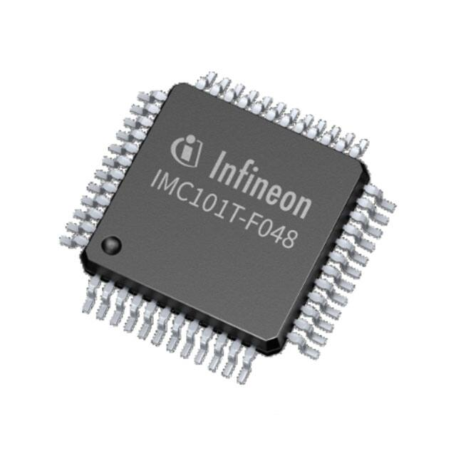


 工商网监
湘ICP备2023018690号
工商网监
湘ICP备2023018690号
