IR3086APbF
DATA SHEET
XPHASETM PHASE IC WITH OVP, FAULT AND OVERTEMP DETECT
DESCRIPTION
TM
The IR3086A Phase IC combined with an IR XPhase Control IC provides a full featured and flexible way
to implement power solutions for the latest high performance CPUs and ASICs. The “Control” IC provides
overall system control and interfaces with any number of “Phase” ICs which each drive and monitor a single
TM
phase of a multiphase converter. The XPhase architecture results in a power supply that is smaller, less
expensive, and easier to design while providing higher efficiency than conventional approaches.
FEATURES
•
•
•
•
•
•
•
•
•
•
•
•
•
2.5A Average Gate Drive Current
Loss-Less Inductor Current Sense
Internal Inductor DCR Temperature Compensation
Programmable Phase Delay
Programmable Feed-Forward Voltage Mode PWM Ramp
Sub 100ns Minimum Pulse Width supports 1MHz per-phase operation
Current Sense Amplifier drives a single wire Average Current Share Bus
Current Share Amplifier reduces PWM Ramp slope to ensure sharing between phases
TM
Body Braking disables Synchronous MOSFET for improved transient response and prevents negative
output voltage at converter turn-off
OVP comparator with 150ns response
Phase Fault Detection
Programmable Phase Over-Temperature Detection
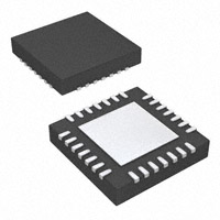
Small thermally enhanced 20L MLPQ package
APPLICATION CIRCUIT
VGATE
12V
PHASE FAULT
RCS-
VRHOT
CCS+
DAC
CCS-
RPHASE3
EA
Page 1 of 33
CSCOMP
16
CSIN+
18
17
CSIN-
DACIN
CBST
CIN
GATEH
PGND
GATEL
15
14
L
13
VO
12
CO
11
VCC
LGND
VCCL
10
6
SCOMP
RPHASE2
ISHARE
9
VRHOT
PWMRMP
5
ISHARE
HOTSET
EAIN
4
DBST
VCCH
IR3086A
PHASE
IC
RMPIN-
8
3
RMPIN+
CPWMRMP
2
RAMP
PHSFLT
20
BIASIN
RPHASE1
5 Wire Analog Bus
From Control IC
19
BIAS
1
RCS+
20k
7
RBIASIN
CVCCL
RVCC
RPWMRMP
CVCC
May 13, 2009
�IR3086APbF
ORDERING INFORMATION
Device
Order Quantity
IR3086AMTRPBF
3000 per reel
* IR3086AMPBF
100 piece strips
* Samples only
ABSOLUTE MAXIMUM RATINGS
o
Operating Junction Temperature……………..150 C
o
o
Storage Temperature Range………………….-65 C to 150 C
ESD Rating………………………………………HBM Class 1C JEDEC standard
PIN #
PIN NAME
VMAX
VMIN
ISOURCE
ISINK
1
2
3
4
5
6
RMPIN+
RMPINHOTSET
VRHOT
ISHARE
SCOMP
20V
20V
20V
20V
20V
20V
-0.3V
-0.3V
-0.3V
-0.3V
-0.3V
-0.3V
1mA
1mA
1mA
1mA
5mA
1mA
1mA
1mA
1mA
30mA
5mA
1mA
7
8
9
10
11
EAIN
PWMRMP
LGND
VCC
VCCL
20V
20V
n/a
24V
27V
-0.3V
-0.3V
n/a
-0.3V
-0.3V
1mA
1mA
50mA
n/a
n/a
1mA
20mA
n/a
50mA
3A for 100ns,
200mA DC
12
GATEL
27V
-0.3V DC, -2V for
100ns
3A for 100ns,
200mA DC
3A for 100ns,
200mA DC
13
PGND
0.3V
-0.3V
n/a
14
GATEH
27V
-0.3V DC, -2V for
100ns
3A for 100ns,
200mA DC
3A for 100ns,
200mA DC
15
VCCH
27V
-0.3V
n/a
16
17
CSIN+
CSIN-
20V
20V
-0.3V
-0.3V
1mA
1mA
3A for 100ns,
200mA DC
1mA
1mA
18
19
20
PHSFLT
DACIN
BIASIN
20V
20V
20V
-0.3V
-0.3V
-0.3V
1mA
1mA
1mA
20mA
1mA
1mA
Page 2 of 33
3A for 100ns,
200mA DC
May 13, 2009
�IR3086APbF
ELECTRICAL SPECIFICATIONS
Unless otherwise specified, these specifications apply over: 8.4V ≤ VCC ≤ 14V, 6V ≤ VCCH ≤ 25V, 6V ≤
o
o
VCCL ≤ 14V, 5.9V ≤ V(BIASIN) ≤ 7.1V, 0.8V ≤ V(DACIN) ≤ 1.6V, and 0 C ≤ TJ ≤ 125 C, CGATEH = 3.3nF,
CGATEL = 6.8nF
PARAMETER
Gate Drivers
GATEH Rise Time
GATEH Fall Time
GATEL Rise Time
GATEL Fall Time
GATEL low to GATEH high
delay
GATEH low to GATEL high
delay
Disable Pull-Down Current
Current Sense Amplifier
CSIN+ Bias Current
CSIN- Bias Current
Input Offset Voltage
TEST CONDITION
VCCH = 12V, Measure 2V to 9V
transition time
VCCH = 12V, Measure 9V to 2V
transition time
VCCL = 12V, Measure 2V to 9V
transition time
VCCL = 12V, Measure 9V to 2V
transition time
VCCH = VCCL = 12V, Measure the time
from GATEL falling to 1V to GATEH
rising to 1V
VCCH = VCCL = 12V, Measure the time
from GATEH falling to 1V to GATEL
rising to 1V
Force GATEH or GATEL = 2V with
BIASIN = 0V
CSIN+ = CSIN- = DACIN. Measure input
referred offset from DACIN
o
Gain at TJ = 25 C
o
Gain at TJ = 125 C
Slew Rate
Differential Input Range
Common Mode Input Range
o
Rout at TJ = 25 C
o
Rout at TJ = 125 C
Ramp Comparator
Input Offset Voltage
Hysteresis
RMPIN+, RMPIN- Bias Current
Propagation Delay
Percentage of Common Mode
Input Voltage Range
Page 3 of 33
MIN
TYP
MAX
UNIT
22
50
ns
22
50
ns
50
75
ns
50
75
ns
10
25
50
ns
10
25
50
ns
15
25
40
µA
-0.5
-1
-3
-0.25
-0.4
0.5
0
0
5
µA
µA
mV
32
27
34
29
12.5
36
31
V/V
V/V
Current Sense Amplifier output is an
internal node. Slew rate at the ISHARE
pin will be set by the internal 10kΩ
resistor and any stray external
capacitance
Note 1
VCCH = 12V. Measure time from
RMPIN input (50mV overdrive) to
GATEL transition to
V(DACIN) (200mV overdrive) to GATEL
transition to > BIAS VOLTAGE
VOUT SENSE+
>> PHASE TIMING
VID2
> PWM CONTROL
VID4
>> VID VOLTAGE
CURRENT SHARE
IR3086A
PHASE IC
VOUT+
0.1uF
COUT
VOUT-
PHASE HOT
CCS
RCS
VOUT SENSE-
PHASE FAULT
CURRENT SHARE
IR3086A
PHASE IC
0.1uF
PHASE HOT
CCS
RCS
ADDITIONAL PHASES
CONTROL BUS
INPUT/OUTPUT
Figure 1. System Block Diagram
Page 6 of 33
May 13, 2009
�IR3086APbF
PWM Control Method
TM
The PWM block diagram of the XPhase architecture is shown in Figure 2. Feed-forward voltage mode control with
trailing edge modulation is used. A high-gain wide-bandwidth voltage type error amplifier in the Control IC is used
for the voltage control loop. An external RC circuit connected to the input voltage and ground is used to program the
slope of the PWM ramp and to provide the feed-forward control at each phase. The PWM ramp slope will change
with the input voltage and automatically compensate for changes in the input voltage. The input voltage can change
due to variations in the silver box output voltage or due to the wire and PCB-trace voltage drop related to changes
in load current.
VIN
CONTROL IC
RAMP GENERATOR
VPEAK
RAMPIN+
RMPOUT
RPHS1
PWM
LATCH
CLOCK
PULSE
GENERATOR
+
RAMPIN-
VVALLEY
-
EAIN
-
-
+
CPWMRMP
EAOUT
SCOMP
X
0.91
-
SHARE
ADJUST
ERROR
AMPLIFIER
CSCOMP
+
+
-
ERROR
AMP
RVFB
CURRENT
SENSE
AMPLIFIER
+
ISHARE
FB
10K
20mV
IROSC
RDRP
VDRP
AMP
CSIN+
+
IFB
VOSNS-
VDAC
BODY
BRAKING
COMPARATOR
+
RAMP
DISCHARGE
CLAMP
VOSNS-
-
GATEL
ENABLE
PWMRMP
+
RPWMRMP
VOUT
COUT
R
GND
RPHS2
VDAC
VBIAS
REGULATOR
VOSNS+
RESET
DOMINANT
+
VBIAS
+
GATEH
S
PWM
COMPARATOR
X34
CCS
RCS
CCS
RCS
-
50%
DUTY
CYCLE
PHASE IC
SYSTEM
REFERENCE
VOLTAGE
BIASIN
CSIN-
DACIN
VDRP
+
-
IIN
PWM
LATCH
CLOCK
PULSE
GENERATOR
+
RAMPIN+
RPHS1
PHASE IC
SYSTEM
REFERENCE
VOLTAGE
BIASIN
-
RAMPIN-
GATEH
S
PWM
COMPARATOR
-
EAIN
RESET
DOMINANT
R
GATEL
+
RPHS2
ENABLE
PWMRMP
+
RPWMRMP
-
X
0.91
-
+
SHARE
ADJUST
ERROR
AMPLIFIER
+
ISHARE
10K
20mV
CURRENT
SENSE
AMPLIFIER
-
CSIN+
+
X34
-
CSCOMP
-
CPWMRMP
BODY
BRAKING
COMPARATOR
+
RAMP
DISCHARGE
CLAMP
SCOMP
CSIN-
DACIN
Figure 2. PWM Block Diagram
Frequency and Phase Timing Control
An oscillator with programmable frequency is located in the Control IC. The output of the oscillator is a 50% duty
cycle triangle waveform with peak and valley voltages of approximately 5V and 1V respectively. This signal is used
to program both the switching frequency and phase timing of the Phase ICs. The Phase IC is programmed by
resistor divider RPHS1 and RPHS2 connected between the VBIAS reference voltage and the Phase IC LGND pin. A
comparator in the Phase ICs detects the crossing of the oscillator waveform over the voltage generated by the
resistor divider and triggers a clock pulse that starts the PWM cycle. The peak and valley voltages track the VBIAS
voltage reducing potential Phase IC timing errors. Figure 3 shows the Phase timing for an 8 phase converter. Note
that both slopes of the triangle waveform can be used for phase timing by swapping the RMPIN+ and RMPIN– pins,
as shown in Figure 2.
Page 7 of 33
May 13, 2009
�IR3086APbF
50% RAMP
DUTY CYCLE
RAMP (FROM
CONTROL IC)
SLOPE = 80mV / % DC
VPEAK (5.0V)
VPHASE4&5 (4.5V)
SLOPE = 1.6mV / ns @ 200kHz
SLOPE = 8.0mV / ns @ 1MHz
VPHASE3&6 (3.5V)
VPHASE2&7 (2.5V)
VPHASE1&8 (1.5V)
VVALLEY (1.00V)
CLK1
PHASE IC CLOCK PULSES
CLK2
CLK3
CLK4
CLK5
CLK6
CLK7
CLK8
Figure 3. 8 Phase Oscillator Waveforms
PWM Operation
The PWM comparator is located in the Phase IC. Upon receiving a clock pulse, the PWM latch is set; the PWMRMP
voltage begins to increase; the low side driver is turned off, and the high side driver is then turned on after the nonoverlap time. When the PWMRMP voltage exceeds the Error Amplifier’s output voltage, the PWM latch is reset.
This turns off the high side driver and turns on the low side driver after the non-overlap time; it activates the Ramp
Discharge Clamp, which quickly discharges the PWMRMP capacitor to the VDAC voltage of the Control IC until the
next clock pulse.
The PWM latch is reset dominant allowing all phases to go to zero duty cycle within a few tens of nanoseconds in
response to a load step decrease. Phases can overlap and go to 100% duty cycle in response to a load step
increase with turn-on gated by the clock pulses. An Error Amplifier output voltage greater than the common mode
input range of the PWM comparator results in 100% duty cycle regardless of the voltage of the PWM ramp. This
arrangement guarantees the Error Amplifier is always in control and can demand 0 to 100% duty cycle as required.
It also favors response to a load step decrease which is appropriate given the low output to input voltage ratio of
most systems. The inductor current will increase much more rapidly than decrease in response to load transients.
This control method is designed to provide “single cycle transient response” where the inductor current changes in
response to load transients within a single switching cycle maximizing the effectiveness of the power train and
minimizing the output capacitor requirements. An additional advantage of the architecture is that differences in
ground or input voltage at the phases have no effect on operation since the PWM ramps are referenced to VDAC.
Figure 4 depicts PWM operating waveforms under various conditions.
Page 8 of 33
May 13, 2009
�IR3086APbF
PHASE IC
CLOCK
PULSE
EAIN
PWMRMP
VDAC
91% VDAC
GATEH
GATEL
STEADY-STATE
OPERATION
DUTY CYCLE DECREASE
DUE TO VIN INCREASE
(FEED-FORWARD)
DUTY CYCLE INCREASE
DUE TO LOAD
INCREASE
DUTY CYCLE DECREASE DUE TO LOAD
DECREASE (BODY BRAKING) OR FAULT
(VCC UV, VCCVID UV, OCP, VID=11111X)
STEADY-STATE
OPERATION
Figure 4. PWM Operating Waveforms
Body Braking
TM
In a conventional synchronous buck converter, the minimum time required to reduce the current in the inductor in
response to a load step decrease is;
TSLEW =
L * ( I MAX − I MIN )
VO
The slew rate of the inductor current can be significantly increased by turning off the synchronous rectifier in
response to a load step decrease. The switch node voltage is then forced to decrease until conduction of the
synchronous rectifier’s body diode occurs. This increases the voltage across the inductor from Vo to Vo +
VBODYDIODE. The minimum time required to reduce the current in the inductor in response to a load transient
decrease is now;
TSLEW =
L * ( I MAX − I MIN )
VO + VBODYDIODE
Since the voltage drop in the body diode is often higher than output voltage, the inductor current slew rate can be
TM
increased by 2X or more. This patent pending technique is referred to as “Body Braking ” and is accomplished
TM
through the “Body Braking Comparator” located in the Phase IC. If the Error Amplifier’s output voltage drops
below 91% of the VDAC voltage this comparator turns off the low side gate driver.
Lossless Average Inductor Current Sensing
Inductor current can be sensed by connecting a resistor and a capacitor in parallel with the inductor and measuring
the voltage across the capacitor, as shown in Figure 5. The equation of the sensing network is,
vCS ( s ) = vL ( s )
1
RL + sL
= iL ( s )
1 + sRCS CCS
1 + sRCS CCS
Usually the resistor Rcs and capacitor Ccs are chosen so that the time constant of Rcs and Ccs equals the time
constant of the inductor which is the inductance L over the inductor DCR (RL). If the two time constants match, the
voltage across Ccs is proportional to the current through L, and the sense circuit can be treated as if only a sense
resistor with the value of RL was used. The mismatch of the time constants does not affect the measurement of
inductor DC current, but affects the AC component of the inductor current.
Page 9 of 33
May 13, 2009
�IR3086APbF
vL
iL
Current
Sense Amp
L
RL
RCS
CCS
VO
CO
c
vCS
CSOUT
Figure 5. Inductor Current Sensing and Current Sense Amplifier
The advantage of sensing the inductor current versus high side or low side sensing is that actual output current
being delivered to the load is obtained rather than peak or sampled information about the switch currents. The
output voltage can be positioned to meet a load line based on real time information. Except for a sense resistor in
series with inductor, this is the only sense method that can support a single cycle transient response. Other
methods provide no information during either load increase (low side sensing) or load decrease (high side sensing).
An additional problem associated with peak or valley current mode control for voltage positioning is that they suffer
from peak-to-average errors. These errors will show in many ways but one example is the effect of frequency
variation. If the frequency of a particular unit is 10% low, the peak to peak inductor current will be 10% larger and
the output impedance of the converter will drop by about 10%. Variations in inductance, current sense amplifier
bandwidth, PWM prop delay, any added slope compensation, input voltage, and output voltage are all additional
sources of peak-to-average errors.
Current Sense Amplifier
This is a high speed differential current sense amplifier, as shown in Figure 5. Its gain decreases with increasing
temperature and is nominally 34 at 25ºC and 29 at 125ºC (-1470 ppm/ºC). This reduction of gain tends to
compensate the 3850 ppm/ºC increase in inductor DCR. Since in most designs the Phase IC junction is hotter than
the inductor these two effects tend to cancel such that no additional temperature compensation of the load line is
required.
The current sense amplifier can accept positive differential input up to 100mV and negative up to -20mV before
clipping. The output of the current sense amplifier is summed with the DAC voltage and sent to the Control IC and
other Phases through an on-chip 10KΩ resistor connected to the ISHARE pin. The ISHARE pins of all the phases
are tied together and the voltage on the share bus represents the average current being delivered to the load and is
used by the Control IC for voltage positioning and current limit protection.
Average Current Share Loop
Current sharing between phases of the converter is achieved by the average current share loop in each Phase IC.
The output of the current sense amplifier is compared with the share bus less a 20mV offset. If current in a phase is
smaller than the average current, the share adjust error amplifier of the phase will activate a current source that
reduces the slope of its PWM ramp thereby increasing its duty cycle and output current. The crossover frequency of
the current share loop can be programmed with a capacitor at the SCOMP pin so that the share loop does not
interact with the output voltage loop.
Page 10 of 33
May 13, 2009
�IR3086APbF
IR3086A THEORY OF OPERATION
Block Diagram
The Block diagram of the IR3086A is shown in Fig. 6, and specific features are discussed in the following sections.
RAMP
COMPARATOR
CLOCK
PULSE
GENERATOR
S
PWM
COMPARATOR
-
EAIN
-
-
R
+
SYSTEM
BIASIN
REFERENCE
VOLTAGE
+
GATE
NON-OVERLAP
COMPARATORS
ENABLE
+
BIASIN
GATEH
RESET
DOMINANT
ENABLE
+
PWMRMP
2V
-
+
RMPIN-
VCCH
+
RMPIN+
PWM
LATCH
-
RAMP
DISCHARGE
CLAMP
-
RAMP
SLOPE VDAC
ADJUST
BODY BRAKING
COMPARATOR
VCCL
GATEL
+
-
SHARE
ADJUST
ERROR
SCOMP
AMP
INTERNAL
VCC
CIRCUIT
BIAS
VDAC +
VDAC
VRHOT
COMPARATOR
-
X34
CSIN+
CSINPHSFLT
+
+
DACIN
CURRENT
SENSE
AMP
-
+
VCC
+
-
+
-
HOTSET
125mV
20mV
LGND
VRHOT
OVP
COMPARATOR
+
10K
+
+
-
+
ISHARE
-
VOLTAGE
PROPORTIONAL
TO ABSOLUTE
TEMPERATURE
-
SCOMP
PGND
X
0.91
FAULT
COMPARATOR
Figure 6 – IR3086A Block Diagram
Tri-State Gate Drivers
The gate drivers can deliver up to 3A peak current. An adaptive non-overlap circuit monitors the voltage on the
GATEH and GATEL pins to prevent MOSFET shoot-through current while minimizing body diode conduction.
An Enable signal is provided by the Control IC to the Phase IC without the addition of a dedicated signal line. The
Error Amplifier output of the Control IC drives low in response to any fault condition such as input under voltage or
TM
output overload. The IR3086A Body Braking comparator detects this and drives both gate outputs low. This tristate operation prevents negative inductor current and negative output voltage during power-down.
The Gate Drivers revert to a high impedance “off” state if VCCL and VCCH supply voltages are below the normal
operating range. An 80kΩ resistor is connected across the GATEH/GATEL and PGND pins to prevent the
GATEH/GATEL voltage from rising due to leakage or other causes under these conditions.
Over Voltage Protection (OVP)
The IR3086A includes over-voltage protection that turns on the low side MOSFET to protect the load in the event of
a shorted high-side MOSFET or connection of the converter output to an excessive output voltage. A comparator
monitors the voltage at the CSIN- pin which is usually connected directly to the converter output. If the voltage
exceeds the DACIN voltage plus 125mV typical (100mV minimum and 160mV maximum) the GATEL pin drives
high. The OVP circuit overrides the normal PWM operation and will fully turn-on the low side MOSFET within
approximately 150ns. The low side MOSFET will remain ON until the over-voltage condition ceases.
Page 11 of 33
May 13, 2009
�IR3086APbF
When designing for OVP the overall system must be considered. In many cases the over-current protection of the
AC-DC or DC-DC converter supplying the multiphase converter will be triggered thus providing effective protection
without damage as long as all PCB traces and components are sized to handle the worst-case maximum current. If
this is not possible a fuse can be added in the input supply to the multiphase converter. One scenario to be careful
of is where the input voltage to the multiphase converter may be pulled below the level where the ICs can provide
adequate voltage to the low side MOSFET thus defeating OVP.
Dynamic changes in the VID code to a lower output voltage may trigger OVP. For example; a 250mV decrease in
output voltage combined with a light load condition will cause the low side MOSFETs to turn on and interfere with
TM
TM
Body Braking . This will not cause a problem, however, as Body Braking will resume once the output voltage is
less than 125mV above the VID voltage.
Since CSIN- pin is also used as the inductor current sensing input, it is usually connected to the local converter
output, which may be far away from the load of the multiphase converter. Excessive distribution impedance
between the converter and load may trigger OVP during normal operation. If the voltage drop across the distribution
impedance exceeds the minimum OVP comparator threshold of 100mV plus VID offset and voltage positioning, the
IR3086A can not be used. The IR3088 Phase IC without OVP should be used instead in applications with excessive
distribution impedance and very small or no AVP. For example, a converter having 25mV of VID offset, 125mV of
AVP at full load, and 100mV of drop in the distribution path at full load would be OK, since 100mV + 25mV + 125mV
= 250mV which is greater than the 100mV drop. However, a converter having 25mV of VID offset, no AVP, and
130mV of drop in the distribution path would require IR3088, since 100mV + 25mV + 0mV = 125mV which is smaller
than the 130mV drop.
Converter with programmable higher output voltage than VID voltage may also trigger OVP during normal
operation, and IR3088 should be used to replace IR3086A.
Thermal Monitoring (VRHOT)
The IR3086A senses its own die temperature and produces a voltage at the input of the VRHOT comparator that is
proportional to temperature. An external resistor divider connected from VBIAS to the HOTSET pin and ground can
be used to program the thermal trip point of the VRHOT comparator. The VRHOT pin is an open-collector output
and should be pulled up to a voltage source through a resistor. If the thermal trip point is reached the VRHOT output
drives low.
Phase Fault
It is possible for multiphase converters to appear to be working correctly with one or more phases not functioning.
The output voltage can still be regulated and the full load current may still be delivered. However, the remaining
phase(s) will be stressed far beyond their intended design limits and are likely to fail. Loss of a phase can occur due
to poor solder connections or mounting during the manufacturing process, or can occur in the field. The most
common failure mode of a buck converter is failure of the high side MOSFET.
The IR3086A has the ability to detect if a phase stops switching and can provide this information to the system
through the PHSFLT output pin. If a phase stops switching its output current will drop to zero and the output of the
current sense amplifier will be the DACIN voltage. The Share Adjust Amplifier reacts to this by increasing the Ramp
Slope Adjust current until it exceeds the externally programmable PWM Ramp bias current. This will cause the
voltage at the PWMRMP pin to drop below its normal operating range. The Fault Comparator trips and drives the
PHSFLT output to ground when the voltage on the PWMRMP pin falls below 91% of the DACIN voltage. PHSFLT is
an open-collector output and should be pulled up to a voltage source through a resistor.
Page 12 of 33
May 13, 2009
�IR3086APbF
APPLICATION INFORMATION
POWERGOOD
VRHOT
PHASE FAULT
12V
RCSQGATE
VGATE
RVCC
10 ohm
CCS+
CCSRBIASIN
RCS+
20k
DBST
16
18
17
CSIN+
13
VOUT+
12
DISTRIBUTION
IMPEDANCE
11
COUT
VOUTVCC
LGND
PWMRMP
CVCCL
RVCC
10
EAIN
SCOMP
7
6
RPHASE13
L
VOUT SENSE-
RPWMRMP
19
RCP
18
CCP
RCS-
RDRP1 CDRP
16
CCS+
CCP1
CCS-
15
RBIASIN
RCS+
20k
VRHOT
CSIN+
16
17
CSIN-
DACIN
ISHARE
SCOMP
RPHASE22
6
RPHASE23
CIN
CSCOMP
GATEH
PGND
GATEL
VCCL
15
14
L
13
12
11
VCC
HOTSET
10
4
CBST
VCCH
IR3086A
PHASE
IC
RMPIN-
LGND
RSHARE
5
CVDAC
RMPIN+
9
RVDAC
19
20
3
ROSC
PHSFLT
BIASIN
2
PWMRMP
1
EAIN
ROCSET
8
RDRP
18
DBST
VDAC
ROSC
TRM4
14
17
14
8
OCSET
GATEL
VOUT SENSE+
15
CVCC
7
IIN
CSCOMP
PGND
CPWMRMP
FB
VDRP
RBBDRP
GATEH
VCCL
CPWMRMP 8
RPHASE12
22
VCC
EAOUT
VID3
VID4
RFB
21
20
ISHARE
RPHASE21
CSS/DEL
23
LGND
RMPOUT
27
26
24
25
SS/DEL
PWRGD
N/C
VID2
13
VID4
7
BBFB
VID1
TRM3
6
VBIAS
IR3081A
CONTROL
IC
VID0
12
VID3
RFB1
VID5
11
5
VOSNS-
4
VID2
TRM2
3
VID1
TRM1
VID0
OSCDS
9
VID5
2
10
1
ENABLE
28
RBBFB
CSIN-
20
VRHOT
5
9
HOTSET
4
CFB
CIN
VCCH
IR3086A
PHASE
IC
RMPIN-
3
0. 1uF
CBST
RMPIN+
2
ENABLE
DACIN
BIASIN
1
PHSFLT
RPHASE11
CVCC
0.1uF
19
DGATE
RGATE
CVCCL
RVCC
RPWMRMP
CVCC
RCSCCS+
CCSRBIASIN
RCS+
20k
16
CSIN+
CSIN-
19
17
20
CSCOMP
GATEH
PGND
GATEL
15
14
L
13
12
11
10
VCC
VCCL
LGND
SCOMP
EAIN
ISHARE
6
RPHASE33
DACIN
BIASIN
VRHOT
PWMRMP
HOTSET
RPHASE32
5
CIN
VCCH
IR3086A
PHASE
IC
RMPIN-
9
4
RMPIN+
7
3
CPWMRMP 8
2
PHSFLT
RPHASE31
1
18
DBST
CBST
CVCCL
RVCC
RPWMRMP
CVCC
RCSCCS+
CCSRBIASIN
RCS+
20k
16
CSIN+
CSIN-
19
17
20
CSCOMP
GATEH
PGND
GATEL
15
14
L
13
12
11
10
VCC
VCCL
LGND
SCOMP
EAIN
ISHARE
6
RPHASE43
DACIN
BIASI N
VRHOT
PWMRMP
HOTSET
RPHASE42
5
CIN
VCCH
IR3086A
PHASE
IC
RMPIN-
9
4
RMPIN+
7
3
CPWMRMP 8
2
PHSFLT
RPHASE41
1
18
DBST
CBST
CVCCL
RVCC
RPWMRMP
CVCC
RCSCCS+
CCSRBIASIN
RCS+
20k
16
CSIN+
CSIN-
19
17
20
CIN
CSCOMP
GATEH
PGND
GATEL
15
14
L
13
12
11
10
VCC
VCCL
LGND
SCOMP
EAIN
ISHARE
6
RPHASE53
DACIN
BIASIN
VRHOT
PWMRMP
HOTSET
RPHASE52
5
9
4
CBST
VCCH
IR3086A
PHASE
IC
RMPIN-
7
3
RMPIN+
CPWMRMP 8
2
PHSFLT
RPHASE51
1
18
DBST
RCS+
CVCCL
RVCC
RPWMRMP
CVCC
RCSCCS+
CCSRBIASIN
RCS+
20k
RPHASE63
16
CSIN+
CSIN-
20
17
19
DACIN
BI ASIN
CIN
GATEH
PGND
GATEL
15
14
L
13
12
11
VCC
VCCL
10
SCOMP
6
CSCOMP
EAIN
ISHARE
LGND
VRHOT
PWMRMP
HOTSET
RPHASE62
5
9
4
CBST
VCCH
IR3086A
PHASE
IC
RMPIN-
7
3
RMPIN+
CPWMRMP 8
2
PHSFLT
RPHASE61
1
18
DBST
RCS+
CVCCL
RVCC
RPWMRMP
CVCC
Figure 7. IR3081A/IR3086A Six-Phase VRM/EVRD 10 Converter
Page 13 of 33
May 13, 2009
�IR3086APbF
DESIGN PROCEDURES – IR3081A AND IR3086A CHIPSET
IR3081A EXTERNAL COMPONENTS
Oscillator Resistor Rosc
The oscillator of IR3081A generates a triangle waveform to synchronize the phase ICs, and the switching frequency
of the each phase converter equals the oscillator frequency, which is set by the external resistor ROSC according to
the curve in Figure 13 of IR3081A Data Sheet.
Soft Start Capacitor CSS/DEL
Because the capacitor CSS/DEL programs four different time parameters, i.e. soft start delay time, soft start time,
over-current latch delay time, and power good delay time, they should be considered together while choosing
CSS/DEL.
The SS/DEL pin voltage controls the slew rate of the converter output voltage, as shown in Figure 10 of IR3081A.
After the ENABLE pin voltage rises above 0.6V, there is a soft-start delay time tSSDEL, after which the error amplifier
output is released to allow the soft start. The soft start time tSS represents the time during which converter voltage
rises from zero to VO. tSS can be programmed by an external capacitor, which is determined by Equation (1).
C SS / DEL =
I CHG * t SS 70 * 10 −6 * t SS
=
VO
VO
(1)
Once CSS/DEL is chosen, the soft start delay time tSSDEL, the over-current fault latch delay time tOCDEL, and the
delay time tVccPG from output voltage (VO) in regulation to Power Good are fixed and shown in Equations (2), (3)
and (4) respectively.
tSSDEL =
CSS / DEL *1.3 CSS / DEL *1.3
=
I CHG
70 *10−6
(2)
tOCDEL =
CSS / DEL * 0.115 CSS / DEL * 0.115
=
I OCDISCHG
40 *10 −6
(3)
CSS / DEL * (3.8 − 0.065 − VO − 1.3) CSS / DEL * (3.735 − VO − 1.3)
=
I CHG
70 *10−6
tVccPG =
(4)
VDAC Slew Rate Programming Capacitor CVDAC and Resistor RVDAC
The slew rate of VDAC down-slope SRDOWN can be programmed by the external capacitor CVDAC as defined in
Equation (5), where ISINK is the sink current of VDAC pin as shown in Figure 15 of IR3081A Data Sheet. The
resistor RVDAC is used to compensate VDAC circuit and is determined by Equation (6). The slew rate of VDAC upslope SRUP is proportional to that of VDAC down-slope and is given by Equation (7), where ISOURCE is the source
current of VDAC pin as shown in Figure15 of IR3081A Data Sheet.
CVDAC =
I SINK
SR DOWN
RVDAC = 0.5 +
SRUP =
Page 14 of 33
3.2 ∗ 10 −15
CVDAC 2
I SOURCE
CVDAC
(5)
(6)
(7)
May 13, 2009
�IR3086APbF
Over Current Setting Resistor ROCSET
The inductor DC resistance is utilized to sense the inductor current. The copper wire of inductor has a constant
temperature coefficient of 3850 ppm/°C, and therefore the maximum inductor DCR can be calculated from Equation
(8), where RL_MAX and RL_ROOM are the inductor DCR at maximum temperature TL_MAX and room temperature
T_ROOM respectively.
R L _ MAX = R L _ ROOM ∗ [1 + 3850 * 10 −6 ∗ (TL _ MAX − TROOM )]
(8)
The current sense amplifier gain decreases with temperature at the rate of 1470 ppm/°C, which compensates part
of the inductor DCR increase. The phase IC die temperature is only a couple of degrees Celsius higher than the
PCB temperature due to the low thermal impedance of MLPQ package. The minimum current sense amplifier gain
at the maximum phase IC temperature TIC_MAX is calculated from Equation (9).
GCS _ MIN = GCS _ ROOM ∗ [1 − 1470 * 10 −6 ∗ (TIC _ MAX − TROOM )]
(9)
The total input offset voltage (VCS_TOFST) of current sense amplifier in phase ICs is the sum of input offset
(VCS_OFST) of the amplifier itself and that created by the amplifier input bias currents flowing through the current
sense resistors RCS+ and RCS-.
VCS _ TOFST = VCS _ OFST + I CSIN + ∗ RCS + − I CSIN − ∗ RCS −
(10)
The over current limit is set by the external resistor ROCSET as defined in Equation (11), where ILIMIT is the required
over current limit. IOCSET, the bias current of OCSET pin, changes with switching frequency setting resistor ROSC
and is determined by the curve in Figure 14 of IR3081A Data Sheet. KP is the ratio of inductor peak current over
average current in each phase and is calculated from Equation (12).
ROCSET = [
KP =
I LIMIT
∗ RL _ MAX ∗ (1 + K P ) + VCS _ TOFST ] ∗ GCS _ MIN / I OCSET
n
(VI − VO ) ∗ VO /( L ∗ VI ∗ f SW ∗ 2)
IO / n
(11)
(12)
No Load Output Voltage Setting Resistor RFB and Adaptive Voltage Positioning Resistor RDRP
A resistor between FB pin and the converter output is used to create output voltage offset VO_NLOFST, which is the
difference between VDAC voltage and output voltage at no load condition. Adaptive voltage positioning further
lowers the converter voltage by RO*IO, where RO is the required output impedance of the converter.
RFB is not only determined by IFB, the current flowing out of FB pin as shown in Figure 14 of IR3081A Data Sheet,
but also affected by the adaptive voltage positioning resistor RDRP and total input offset voltage of current sense
amplifiers. RFB and RDRP are determined by (13) and (14) respectively.
R FB =
R L _ MAX ∗ VO _ NLOFST − VCS _ TOFST ∗ n ∗ RO
R DRP =
Body Braking
TM
I FB ∗ R L _ MAX
R FB ∗ R L _ MAX ∗ GCS _ MIN
n ∗ RO
(13)
(14)
Related Resistors RBBFB and RBBDRP
TM
The Body Braking during Dynamic VID can be disabled by connecting BBFB pin to ground. If the feature is
enabled, Resistors RBBFB and RBBDRP are needed to restore the feedback voltage of the error amplifier after
Dynamic VID step down. Usually RBBFB and RBBDRP are chosen to match RFB and RDRP respectively.
Page 15 of 33
May 13, 2009
�IR3086APbF
IR3086A EXTERNAL COMPONENTS
PWM Ramp Resistor RPWMRMP and Capacitor CPWMRMP
PWM ramp is generated by connecting the resistor RPWMRMP between a voltage source and PWMRMP pin as well
as the capacitor CPWMRMP between PWMRMP and LGND. Choose the desired PWM ramp magnitude VRAMP and
the capacitor CPWMRMP in the range of 100pF and 470pF, and then calculate the resistor RPWMRMP from Equation
(15). To achieve feed-forward voltage mode control, the resistor RRAMP should be connected to the input of the
converter.
VO
(15)
RPWMRMP =
VIN * f SW * CPWMRMP * [ln(VIN − VDAC ) − ln(VIN − VDAC − VPWMRMP )]
Inductor Current Sensing Capacitor CCS+ and Resistors RCS+ and RCSThe DC resistance of the inductor is utilized to sense the inductor current. Usually the resistor RCS+ and capacitor
CCS+ in parallel with the inductor are chosen to match the time constant of the inductor, and therefore the voltage
across the capacitor CCS+ represents the inductor current. If the two time constants are not the same, the AC
component of the capacitor voltage is different from that of the real inductor current. The time constant mismatch
does not affect the average current sharing among the multiple phases, but affect the current signal ISHARE as well
as the output voltage during the load current transient if adaptive voltage positioning is adopted.
Measure the inductance L and the inductor DC resistance RL. Pre-select the capacitor CCS+ and calculate RCS+ as
follows.
L RL
(16)
RCS + =
C CS +
The bias current flowing out of the non-inverting input of the current sense amplifier creates a voltage drop across
RCS+, which is equivalent to an input offset voltage of the current sense amplifier. The offset affects the accuracy of
converter current signal ISHARE as well as the accuracy of the converter output voltage if adaptive voltage
positioning is adopted. To reduce the offset voltage, a resistor RCS- should be added between the amplifier inverting
input and the converter output. The resistor RCS- is determined by the ratio of the bias current from the non-inverting
input and the bias current from the inverting input.
I
(17)
RCS − = CSIN + ∗ RCS +
I CSIN −
If RCS- is not used, RCS+ should be chosen so that the offset voltage is small enough. Usually RCS+ should be less
than 2 kΩ and therefore a larger CCS+ value is needed.
Over Temperature Setting Resistors RHOTSET1 and RHOTSET2
The threshold voltage of VRHOT comparator is proportional to the die temperature TJ (ºC) of phase IC. Determine
the relationship between the die temperature of phase IC and the temperature of the power converter according to
the power loss, PCB layout and airflow etc, and then calculate HOTSET threshold voltage corresponding to the
allowed maximum temperature from Equation (18).
V HOTSET = 4.73 * 10 −3 * T J + 1.241
(18)
There are two ways to set the over temperature threshold, central setting and local setting. In the central setting,
only one resistor divider is used, and the setting voltage is connected to HOTSET pins of all the phase ICs. To
reduce the influence of noise on the accuracy of over temperature setting, a 0.1uF capacitor should be placed next
to HOTSET pin of each phase IC. In the local setting, a resistor divider per phase is needed, and the setting voltage
is connected to HOTSET pin of each phase. The 0.1uF decoupling capacitor is not necessary. Use VBIAS as the
reference voltage. If RHOTSET1 is pre-selected, RHOTSET2 can be calculated as follows.
R
∗V
(19)
RHOTSET 2 = HOTSET 1 HOTSET
VBIAS − VHOTSET
Page 16 of 33
May 13, 2009
�IR3086APbF
Phase Delay Timing Resistors RPHASE1 and RPHASE2
The phase delay of the interleaved multiphase converter is programmed by the resistor divider connected at
RMPIN+ or RMPIN- depending on which slope of the oscillator ramp is used for the phase delay programming of
phase IC, as shown in Figure 3.
If the upslope is used, RMPIN+ pin of the phase IC should be connected to RMPOUT pin of the control IC and
RMPIN- pin should be connected to the resistor divider. When RMPOUT voltage is above the trip voltage at
RMPIN- pin, the PWM latch is set. GATEL becomes low, and GATEH becomes high after the non-overlap time.
If down slope is used, RMPIN- pin of the phase IC should be connected to RMPOUT pin of the control IC and
RMPIN+ pin should be connected to the resistor divider. When RMPOUT voltage is below the trip voltage at
RMPIN- pin, the PWM latch is set. GATEL becomes low, and GATEH becomes high after the non-overlap time.
Use VBIAS voltage as the reference for the resistor divider since the oscillator ramp magnitude from control IC
tracks VBIAS voltage. Try to avoid both edges of the oscillator ramp for better noise immunity. Determine the ratio
of the programming resistors corresponding to the desired switching frequencies and phase numbers. If the resistor
RPHASEx1 is pre-selected, the resistor RPHASEx2 is determined as:
R PHASEx 2 =
RAPHASEx ∗ R PHASEx1
1 − RAPHASEx
(20)
Combined Over Temperature and Phase Delay Setting Resistors RPHASE1, RPHASE2 and RPHASE3
The over temperature setting resistor divider can be combined with the phase delay resistor divider to save one
resistor per phase.
Calculate the HOTSET threshold voltage VHOTSET corresponding to the allowed maximum temperature from
Equation (18). If the over temperature setting voltage is lower than the phase delay setting voltage,
VBIAS*RAPHASEx, connect RMPIN+ or RMPIN- pin between RPHASEx1 and RPHASEx2, and connect HOTSET pin
between RPHASEx2 and RPHASEx3. Pre-select RPHASEx1,
RPHASEx 2 =
( RAPHASEx ∗ VBIAS − VHOTSET ) * RPHASEx1
VBIAS ∗ (1 − RAPHASEx )
(21)
RPHASEx 3 =
VHOTSET ∗ RPHASEx1
VBIAS * (1 − RAPHASEx )
(22)
If the over temperature setting voltage is higher than the phase delay setting voltage, VBIAS*RAPHASEx, connect
HOTSET pin between RPHASEx1 and RPHASEx2, and connect RMPIN+ or RMPIN- between RPHASEx2 and RPHASEx3.
Pre-select RPHASEx1,
R PHASEx 2 =
(V HOTSET − RAPHASEx ∗ V BIAS ) ∗ R PHASEx1
V BIAS − V HOTSET
(23)
RPHASEx 3 =
RAPHASEx ∗ VBIAS * RPHASEx1
VBIAS − VHOTSET
(24)
Bootstrap Capacitor CBST
Depending on the duty cycle and gate drive current of the phase IC, a 0.1uF to 1uF capacitor is needed for the
bootstrap circuit.
Decoupling Capacitors for Phase IC
0.1uF-1uF decoupling capacitors are required at VCC and VCCL pins of phase ICs.
Page 17 of 33
May 13, 2009
�IR3086APbF
VOLTAGE LOOP COMPENSATION
The adaptive voltage positioning (AVP) is usually adopted in the computer applications to improve the transient
response and reduce the power loss at heavy load. Like current mode control, the adaptive voltage positioning loop
introduces extra zero to the voltage loop and splits the double poles of the power stage, which make the voltage
loop compensation much easier.
Resistors RFB and RDRP are chosen according to Equations (13) and (14), and the selection of compensation types
depends on the output capacitors used in the converter. For the applications using Electrolytic, Polymer or ALPolymer capacitors and running at lower frequency, type II compensation shown in Figure 8(a) is usually enough.
While for the applications using only ceramic capacitors and running at higher frequency, type III compensation
shown in Figure 8(b) is preferred.
For applications where AVP is not required, the compensation is the same as for the regular voltage mode control.
For converter using Polymer, AL-Polymer, and ceramic capacitors, which have much higher ESR zero frequency,
type III compensation is required as shown in Figure 8(b) with RDRP and CDRP removed.
CCP1
CCP1
RFB
RCP
CCP
VO+
RCP
CCP
RFB1
CFB
FB
-
RFB
VO+
FB
-
RDRP
EAOUT
VDAC
RDRP
VDRP
EAOUT
EAOUT
+
(a) Type II compensation
EAOUT
VDAC
VDRP
+
CDRP
(b) Type III compensation
Figure 8. Voltage loop compensation network
Type II Compensation for AVP Applications
Determine the compensation at no load, the worst case condition. Choose the crossover frequency fc between 1/10
and 1/5 of the switching frequency per phase. Assume the time constant of the resistor and capacitor across the
output inductors matches that of the inductor, and determine RCP and CCP from Equations (25) and (26), where LE
and CE are the equivalent inductance of output inductors and the equivalent capacitance of output capacitors
respectively.
( 2π ∗ fC ) 2 ∗ LE ∗ CE ∗ RFB ∗ VPWMRMP
(25)
RCP =
VO * 1 + ( 2π * fC * C * RC ) 2
CCP =
10 ∗ LE ∗ C E
RCP
(26)
CCP1 is optional and may be needed in some applications to reduce the jitter caused by the high frequency noise. A
ceramic capacitor between 10pF and 220pF is usually enough.
Type III Compensation for AVP Applications
Determine the compensation at no load, the worst case condition. Assume the time constant of the resistor and
capacitor across the output inductors matches that of the inductor, the crossover frequency and phase margin of the
voltage loop can be estimated by Equations (27) and (28), where RLE is the equivalent resistance of inductor DCR.
f C1 =
Page 18 of 33
RDRP
2π * CE ∗ GCS * RFB ∗ RLE
(27)
May 13, 2009
�IR3086APbF
θ C1 = 90 − A tan(0.5) ∗
180
(28)
π
Choose the desired crossover frequency fc around fc1 estimated by Equation (27) or choose fc between 1/10 and
1/5 of the switching frequency per phase, and select the components to ensure the slope of close loop gain is -20dB
/Dec around the crossover frequency. Choose resistor RFB1 according to Equation (29), and determine CFB and
RDRP from Equations (30) and (31).
1
R FB
2
R FB1 =
to
R FB1 =
2
R FB
3
1
CFB =
(29)
(30)
4π ∗ fC ∗ RFB1
( R FB + R FB1 ) ∗ C FB
(31)
R DRP
RCP and CCP have limited effect on the crossover frequency, and are used only to fine tune the crossover frequency
and transient load response. Determine RCP and CCP from Equations (32) and (33).
C DRP =
RCP =
(2π ∗ fC ) 2 ∗ LE ∗ CE ∗ RFB ∗ VPWMRMP
VO
CCP =
10 ∗ LE ∗ C E
(32)
(33)
RCP
CCP1 is optional and may be needed in some applications to reduce the jitter caused by the high frequency noise. A
ceramic capacitor between 10pF and 220pF is usually enough.
Type III Compensation for Non-AVP Applications
Resistor RFB is chosen according to Equations (13), and resistor RDRP and capacitor CDRP are not needed. Choose
the crossover frequency fc between 1/10 and 1/5 of the switching frequency per phase and select the desired phase
margin θc. Calculate K factor from Equation (34), and determine the component values based on Equations (35) to
(39),
π
θ
K = tan[ ∗ ( C + 1.5)]
4 180
RCP = RFB ∗
(34)
( 2π ∗ LE ∗ CE ∗ fC ) 2 ∗ VPWMRMP
VO ∗ K
(35)
CCP =
K
2π ∗ fC ∗ RCP
(36)
CCP1 =
1
2π ∗ fC ∗ K ∗ RCP
(37)
CFB =
K
2π ∗ fC ∗ RFB
(38)
R FB1 =
Page 19 of 33
1
2π ∗ f C ∗ K ∗ C FB
(39)
May 13, 2009
�IR3086APbF
CURRENT SHARE LOOP COMPENSATION
The crossover frequency of the current share loop should be at least one decade lower than that of the voltage loop
in order to eliminate the interaction between the two loops. A capacitor from SCOMP to ground is usually enough
for the share loop compensation. Choose the crossover frequency of current share loop (fCI) based on the
crossover frequency of voltage loop (fC), and determine the CSCOMP,
CSCOMP =
0.65 * RPWMRMP * VI * I O * GCS _ ROOM * RLE * [1 + 2π * fCI * CE * (VO I O )] * FMI
VO ∗ 2π ∗ fCI *1.05 *106
(40)
Where FMI is the PWM gain in the current share loop,
FMI =
Page 20 of 33
RPWMRMP * CPWMRMP * f SW *V PWMRMP
(VI − VPWMRMP − VDAC ) * (VI − VDAC )
(41)
May 13, 2009
�IR3086APbF
DESIGN EXAMPLE 1 - VRM 10 2U CONVERTER
SPECIFICATIONS
Input Voltage: VI=12 V
DAC Voltage: VDAC=1.35 V
No Load Output Voltage Offset: VO_NLOFST=20 mV
Output Current: IO=105 ADC
Maximum Output Current: IOMAX=120 ADC
Output Impedance: RO=0.91 mΩ
VCC Ready to VCC Power Good Delay: tVccPG=0-10mS
Soft Start Time: tSS=2 mS
Over Current Delay: tOCDEL< 0.5mS
Dynamic VID Down-Slope Slew Rate: SRDOWN=2.5mV/uS
Over Temperature Threshold: TPCB=115 ºC
POWER STAGE
Phase Number: n=6
Switching Frequency: fSW =400 kHz
Output Inductors: L=220 nH, RL=0.47 mΩ
Output Capacitors: AL-Polymer, C=560uF, RC= 7mΩ, Number Cn=10
IR3081A EXTERNAL COMPONENTS
Oscillator Resistor Rosc
Once the switching frequency is chosen, ROSC can be determined from the curve in Figure 13 of IR3081A Data
Sheet. For switching frequency of 400kHz per phase, choose ROSC=30.1kΩ
Soft Start Capacitor CSS/DEL
Determine the soft start capacitor from the required soft start time.
C SS / DEL =
I CHG ∗ t SS 70 *10 −6 ∗ 2 *10 −3
=
= 0.1uF
VO
1.35 − 20 *10 −3
The soft start delay time is
CSS / DEL ∗ 1.3 0.1 *10 −6 ∗1.3
=
= 1.86mS
I CHG
70 *10− 6
tSSDEL =
The power good delay time is
tVccPG =
CSS / DEL * (3.735 − VO − 1.3) 0.1*10−6 * (3.735 − 1.33 − 1.3)
=
= 1.58ms
I CHG
70 *10−6
Over current delay time is
tOCDEL =
CSS / DEL * 0.115 0.1 *10−6 * 0.115
=
= 0.29ms
I OCDISCHG
40 *10−6
Page 21 of 33
May 13, 2009
�IR3086APbF
VDAC Slew Rate Programming Capacitor CVDAC and Resistor RVDAC
From Figure 15 of IR3081A Data Sheet, the sink current of VDAC pin corresponding to 400kHz (ROSC=30.1kΩ) is
76uA. Calculate the VDAC down-slope slew-rate programming capacitor from the required down-slope slew rate.
CVDAC =
I SINK
76 * 10 −6
=
= 30.4nF , Choose CVDAC=33nF
SR DOWN
2.5 * 10 −3 / 10 −6
Calculate the programming resistor.
RVDAC = 0.5 +
3.2 * 10 −15
CVDAC 2
= 0.5 +
3.2 * 10 −15
(33 * 10 −9 ) 2
= 3.5Ω
From Figure 15 or IR3081A Data Sheet, the source current of VDAC pin is 110uA. The VDAC up-slope slew rate is
SRUP =
I SOURCE 110 * 10 −6
=
= 3.3mV / uS
CVDAC
33 * 10 −9
Over Current Setting Resistor ROCSET
The room temperature is 25ºC and the target PCB temperature is 100 ºC. The phase IC die temperature is about 1
ºC higher than that of phase IC, and the inductor temperature is close to PCB temperature.
Calculate Inductor DC resistance at 100 ºC,
RL _ MAX = RL _ ROOM ∗ [1 + 3850*10−6 ∗ (TL _ MAX − TROOM )] = 0.47 *10−3 ∗ [1 + 3850*10−6 ∗ (100 − 25)] = 0.61mΩ
The current sense amplifier gain is 34 at 25ºC, and its gain at 101ºC is calculated as,
G CS _ MIN = G CS _ ROOM ∗ [1 − 1470 *10 −6 ∗ (T IC _ MAX − T ROOM )] = 34 ∗ [1 − 1470 *10 −6 ∗ (101 − 25)] = 30.2
Set the over current limit at 135A. From Figure 14 of IR3081A Data Sheet, the bias current of OCSET pin (IOCSET)
is 41uA with ROSC=30.1kΩ. The total current sense amplifier input offset voltage is 0.55mV, which includes the
offset created by the current sense amplifier input resistor mismatch.
Calculate constant KP, the ratio of inductor peak current over average current in each phase,
KP =
(V I − VO ) ∗ VO /( L ∗ V I ∗ f SW ∗ 2) (12 − 1.33) ∗ 1.33 /( 220 * 10 −9 ∗ 12 ∗ 400 * 10 3 ∗ 2)
=
= 0.3
I LIMIT / n
135 / 6
ROCSET = [
=(
RLIMIT
∗ RL _ MAX ∗ (1 + K P ) + VCS _ TOFST ] ∗ GCS _ MIN / I OCSET
n
135
∗ 0.61 *10 −3 ∗ 1.3 + 0.55 *10 −3 ) ∗ 30.2 /( 41 *10 − 6 ) = 13.3kΩ
6
No Load Output Voltage Setting Resistor RFB and Adaptive Voltage Positioning Resistor RDRP
From Figure 14 of IR3081A Data Sheet, the bias current of FB pin is 41uA with ROSC=30.1kΩ.
R FB =
RDRP =
R L _ MAX ∗ V O _ NLOFST − V CS _ TOFST ∗ n ∗ R O
I FB ∗ R L _ MAX
RFB ∗ RL _ MAX ∗ GCS _ MIN
n ∗ RO
Page 22 of 33
=
=
0 .61 * 10 −3 ∗ 20 * 10 −3 − 0 .55 * 10 −3 ∗ 6 ∗ 0 .91 * 10 −3
41 * 10 − 6 ∗ 0 .61 * 10 − 3
= 365 Ω
365 ∗ 0.61 *10−3 ∗ 30.2
= 1.21kΩ
6 ∗ 0.91 *10−3
May 13, 2009
�IR3086APbF
Body Braking
TM
Related Resistors RBBFB and RBBDRP
N/A. The body braking during Dynamic VID is disabled.
IR3081A EXTERNAL COMPONENTS
PWM Ramp Resistor RPWMRMP and Capacitor CPWMRMP
Set PWM ramp magnitude VPWMRMP=0.8V. Choose 220pF for PWM ramp capacitor CPWMRMP, and calculate the
resistor RPWMRMP,
VO
RPWMRMP =
VIN ∗ f SW ∗ CPWMRMP ∗ [ln(VIN − VDAC ) − ln(VIN − VDAC − VPWMRMP )]
1.33
=
3
12 ∗ 400 *10 ∗ 220 *10
−12
= 16.1kΩ , choose RPWMRMP=16.2kΩ
∗ [ln(12 − 1.35) − ln(12 − 1.35 − 0.8)]
Inductor Current Sensing Capacitor CCS+ and Resistors RCS+ and RCSChoose CCS+=47nF, and calculate RCS+,
RCS + =
L RL 220 *10−9 /(0.47 *10−3 )
=
= 10.0kΩ
CCS +
47 *10 −9
The bias currents of CSIN+ and CSIN- are 0.25uA and 0.4uA respectively. Calculate resistor RCS-,
RCS − =
0.25
0.25
∗ RCS + =
∗ 10.0 *103 = 6.2kΩ , choose RCS-=6.19kΩ
0.4
0.4
Over Temperature Setting Resistors RHOTSET1 and RHOTSET2
Use central over-temperature setting and set the temperature threshold at 115 ºC, which corresponds to the IC die
temperature of 116 ºC. Calculate the HOTSET threshold voltage corresponding to the temperature thresholds.
V HOTSET = 4.73 * 10 −3 * TJ + 1.241 = 4.73 * 10 −3 ∗ 116 + 1.241 = 1.79V
Pre-select RHOTSET1=10.0kΩ,
R HOTSET 2 =
R HOTSET 1 ∗ V HOTSET 10 *10 3 ∗1.79
=
= 3.57 kΩ
V BIAS − V HOTSET
6.8 − 1.79
Phase Delay Timing Resistors RPHASE1 and RPHASE2
Use central over-temperature setting and set the temperature threshold at 115 ºC, which corresponds to the IC die
temperature of 116 ºC. Calculate the HOTSET threshold voltage corresponding to the temperature thresholds.
The phase delay resistor ratios for phases 1 to 6 at 400kHz of switching frequencies are RAPHASE1=0.628,
RAPHASE2=0.415, RAPHASE3=0.202, RAPHASE4=0.246, RAPHASE5=0.441 and RAPHASE6=0.637 starting from downslope. Pre-select RPHASE11=RPHASE21=RPHASE31=RPHASE41=RPHASE51= RPHASE61=10kΩ,
RPHASE12 =
RAPHASE1
0.628
∗ RPHASE11 =
∗ 10 *103 = 16.9kΩ
1 − RAPHASE1
1 − 0.628
RPHASE22=7.15kΩ, RPHASE32=2.55kΩ, RPHASE42=3.24kΩ, PPHASE52=7.87kΩ, RPHASE62=17.4kΩ
Page 23 of 33
May 13, 2009
�IR3086APbF
Bootstrap Capacitor CBST
Choose CBST=0.1uF
Decoupling Capacitors for Phase IC and Power Stage
Choose CVCC=0.1uF, CVCCL=0.1uF
VOLTAGE LOOP COMPENSATION
Type II compensation is used for the converter with AL-Polymer output capacitors. Choose the crossover frequency
fc=40kHz, which is 1/10 of the switching frequency per phase, and determine Rcp and CCP.
RCP =
CCP =
(2π ∗ fC )2 ∗ LE ∗ CE ∗ RFB ∗ VRAMP
VO * 1 + (2π * fC * C * RC )2
10 ∗ LE ∗ CE
RCP
=
=
(2π ∗ 40 ∗103 )2 ∗ (220 ∗10−9 / 6) ∗ (560 ∗10−6 ∗10) ∗ 365 ∗ 0.8
(1.35 − 20 ∗10−3 ) * 1 + (2π * 40 *103 * 560 *10−6 * 7 *10−3 )2
10 ∗ ( 220 ∗ 10−9 / 6) ∗ (560 ∗ 10−6 *10)
2.0 ∗ 103
= 2.0kΩ
= 71nF , Choose CCP=68nF
Choose CCP1=47pF to reduce high frequency noise.
CURRENT SHARE LOOP COMPENSATION
The crossover frequency of the current share loop fCI should be at least one decade lower than that of the voltage
loop fC. Choose the crossover frequency of current share loop fCI=4kHz, and calculate CSCOMP,
FMI =
RPWMRMP * CPWMRMP * f SW *V PWMRMP 16.2 *103 * 220 *10−12 * 400 *103 * 0.8
=
= 0.011
(VI − VPWMRMP − VDAC ) * (VI − VDAC )
(12 − 0.8 − 1.35) * (12 − 1.35)
CSCOMP =
=
0.65 * RPWMRMP * VI * I O * GCS _ ROOM * RLE * [1 + 2π * fCI * CE * (VO I O )] * FMI
VO ∗ 2π ∗ fCI *1.05 *106
0.65 *16.2 *10 3 *12 *105 * 34 * (0.47 *10 −3 6) *[1 + 2π * 4 *10 3 * 560 *10 −6 *10 * (1.33 − 105 * 9.1*10 −4 ) 105] * 0.011
(1.33 − 105 * 9.1*10 − 4 ) ∗ 2π ∗ 4 *10 3 *1.05 *10 6
= 31.4nF
Choose CSCOMP=33nF.
Page 24 of 33
May 13, 2009
�IR3086APbF
DESIGN EXAMPLE 2 - EVRD 10 HIGH FREQUENCY ALL-CERAMIC CONVERTER
SPECIFICATIONS
Input Voltage: VI=12 V
DAC Voltage: VDAC=1.3 V
No Load Output Voltage Offset: VO_NLOFST=20 mV
Output Current: IO=105 ADC
Maximum Output Current: IOMAX=120 ADC
Output Impedance: RO=0.91 mΩ
VCC Ready to VCC Power Good Delay: tVccPG=0-10mS
Soft Start Time: tSS=2.9mS
Over Current Delay: tOCDEL < 0.5mS
Dynamic VID Down-Slope Slew Rate: SRDOWN=2.5mV/uS
Over Temperature Threshold: TPCB=115 ºC
POWER STAGE
Phase Number: n=6
Switching Frequency: fSW =800 kHz
Output Inductors: L=100 nH, RL=0.5 mΩ
Output Capacitors: Ceramic, C=22uF, RC= 2mΩ, Number Cn=62
IR3081A EXTERNAL COMPONENTS
Oscillator Resistor Rosc
Once the switching frequency is chosen, ROSC can be determined from the curve in Figure 13 of IR3081A Data
Sheet. For switching frequency of 800kHz per phase, choose ROSC=13.3kΩ
Soft Start Capacitor CSS/DEL
Determine the soft start capacitor from the required soft start time.
CSS / DEL =
I CHG ∗ tSS 70 *10−6 ∗ 3 *10−3
=
= 0.16uF , choose CSS/DEL=0.15uF
VO
1.3 − 20 *10−3
The soft start delay time is
CSS / DEL ∗ 1.3 0.15 *10−6 ∗ 1.3
=
= 2.8mS
I CHG
70 *10−6
tSSDEL =
The power good delay time is
tVccPG =
CSS / DEL * (3.735 − VO − 1.3) 0.15 *10−6 * (3.735 − 1.33 − 1.3)
=
= 2.4ms
I CHG
70 *10− 6
Over current delay time is
tOCDEL =
CSS / DEL * 0.115 0.15 *10−6 * 0.115
=
= 0.43ms
I OCDISCHG
40 *10− 6
VDAC Slew Rate Programming Capacitor CVDAC and Resistor RVDAC
From Figure 15 of IR3081A Data Sheet, the sink current of VDAC pin corresponding to 800kHz (ROSC=13.3kΩ) is
170uA. Calculate the VDAC down-slope slew-rate programming capacitor from the required down-slope slew rate.
Page 25 of 33
May 13, 2009
�IR3086APbF
CVDAC =
I SINK
170 * 10 −6
=
= 68nF
SR DOWN
2.5 * 10 −3 / 10 −6
Calculate the programming resistor.
RVDAC = 0.5 +
3.2 * 10 −15
CVDAC 2
= 0.5 +
3.2 * 10 −15
(68 * 10 −9 ) 2
= 1.2Ω
From Figure 15 of IR3081A Data Sheet, the source current of VDAC pin is 250uA. The VDAC up-slope slew rate is
SRUP =
I SOURCE 250 *10 −6
=
= 3.7mV / uS
CVDAC
68 *10 −9
Over Current Setting Resistor ROCSET
The room temperature is 25ºC and the target PCB temperature is 100 ºC. The phase IC die temperature is about 1
ºC higher than that of phase IC, and the inductor temperature is close to PCB temperature.
Calculate Inductor DC resistance at 100 ºC,
RL _ MAX = RL _ ROOM ∗ [1 + 3850*10−6 ∗ (TL _ MAX − TROOM )] = 0.5 *10−3 ∗ [1 + 3850*10−6 ∗ (100 − 25)] = 0.64mΩ
The current sense amplifier gain is 34 at 25ºC, and its gain at 101ºC is calculated as,
G CS _ MIN = G CS _ ROOM ∗ [1 − 1470 *10 −6 ∗ (T IC _ MAX − T ROOM )] = 34 ∗ [1 − 1470 *10 −6 ∗ (101 − 25)] = 30.2
Set the over current limit at 135A. From Figure 14 of IR3081A Data Sheet, the bias current of OCSET pin (IOCSET)
is 90uA with ROSC=13.3kΩ. The total current sense amplifier input offset voltage is 0.55mV, which includes the
offset created by the current sense amplifier input resistor mismatch.
Calculate constant KP, the ratio of inductor peak current over average current in each phase,
KP =
(VI − VO ) ∗ VO /( L ∗ VI ∗ f SW ∗ 2) (12 − 1.28) ∗ 1.28 /(100 *10−9 ∗ 12 ∗ 800 *103 ∗ 2)
=
= 0.32
I LIMIT / n
135 / 6
ROCSET = [
=(
RLIMIT
∗ RL _ MAX ∗ (1 + K P ) + VCS _ TOFST ] ∗ GCS _ MIN / I OCSET
n
135
∗ 0.64 *10 −3 ∗ 1.32 + 0.55 *10 − 3 ) * 30.2 /(90 *10 − 6 ) = 6.34 kΩ
6
No Load Output Voltage Setting Resistor RFB and Adaptive Voltage Positioning Resistor RDRP
From Figure 14 of IR3081A Data Sheet, the bias current of FB pin is 90uA with ROSC=13.3kΩ.
RFB =
RL _ MAX ∗ VO _ NLOFST − VCS _ TOFST ∗ n ∗ RO
RDRP =
I FB ∗ RL _ MAX
RFB ∗ RL _ MAX ∗ GCS _ MIN
n ∗ RO
Body Braking
TM
=
=
0.64 *10 −3 ∗ 20 *10−3 − 0.55 *10−3 ∗ 6 ∗ 0.91 *10−3
= 162Ω
90 *10−6 * 0.64 *10−3
162 ∗ 0.64 *10 −3 * 30.2
= 576Ω
6 ∗ 0.91 *10−3
Related Resistors RBBFB and RBBDRP
N/A. The body braking during Dynamic VID is disabled.
Page 26 of 33
May 13, 2009
�IR3086APbF
IR3086A EXTERNAL COMPONENTS
PWM Ramp Resistor RPWMRMP and Capacitor CPWMRMP
Set PWM ramp magnitude VPWMRMP=0.75V. Choose 100pF for PWM ramp capacitor CPWMRMP, and calculate the
resistor RPWMRMP,
VO
RPWMRMP =
VIN * f SW * CPWMRMP * [ln(VIN − VDAC ) − ln(VIN − VDAC − VPWMRMP )]
=
1.28
= 18.2kΩ
3
−
12
12 ∗ 800 *10 ∗ 100 *10
∗ [ln(12 − 1.3) − ln(12 − 1.3 − 0.75)]
Inductor Current Sensing Capacitor CCS+ and Resistors RCS+ and RCSChoose 47nF for capacitor CCS+, and calculate RCS+,
RCS + =
L RL 100 *10 −9 /(0.5 *10−3 )
=
= 4.22kΩ
CCS +
47 *10 −9
The bias currents of CSIN+ and CSIN- are 0.25uA and 0.4uA respectively. Calculate resistor RCS-,
RCS − =
0.25
0.25
∗ RCS + =
∗ 4.22 *10 3 = 2.61kΩ
0.4
0.4
Combined Over Temperature and Phase Delay Setting Resistors RPHASEx1, RPHASEx2 and RPHASEx3
The over temperature setting resistor divider is combined with the phase delay resistor divider. Set the temperature
threshold at 115 ºC, which corresponds to the IC die temperature of 116 ºC, and calculate the HOTSET threshold
voltage corresponding to the temperature thresholds.
V HOTSET = 4.73 * 10 −3 ∗ TJ + 1.241 = 4.73 * 10 −3 ∗ 116 + 1.241 = 1.79V
The phase delay resistor ratios for phases 1 to 6 at 800kHz of switching frequencies are RAPHASE1=0.665,
RAPHASE2=0.432, RAPHASE3=0.198, RAPHASE4=0.206, RAPHASE5=0.401 and RAPHASE6=0.597 starting from downslope.
The over temperature setting voltage of phases 1, 2, 5, and 6 is lower than the phase delay setting voltage,
VBIAS*RAPHASEx. Pre-select RPHASE11=10kΩ,
RPHASEx 2 =
( RAPHASEx ∗ VBIAS − VHOTSET ) * RPHASEx1 (0.665 ∗ 6.8 − 1.79) ∗ 10 *103
=
= 12.1kΩ
VBIAS ∗ (1 − RAPHASEx )
6.8 ∗ (1 − 0.665)
RPHASEx 3 =
VHOTSET ∗ RPHASEx1
1.79 ∗ 12.1 *103
=
= 7.87 kΩ
VBIAS * (1 − RAPHASEx ) 6.8 * (1 − 0.665)
RPHASE21=10kΩ, RPHASE22=2.94kΩ, RPHASE23=4.64kΩ
RPHASE51=10kΩ, RPHASE52=2.32kΩ, RPHASE53=4.42kΩ
RPHASE61=10kΩ, RPHASE62=8.25kΩ, RPHASE63=6.49kΩ
The over temperature setting voltage of Phases 3 and 4 is higher than the phase delay setting voltage,
VBIAS*RAPHASEx. Pre-select RPHASEX1=10kΩ,
R PHASE 32 =
(V HOTSET − RAPHASE 3 ∗ V BIAS ) ∗ R PHASE 31 (1.79 − 0.198 ∗ 6.8) ∗10 *10 3
=
= 887Ω
V BIAS − V HOTSET
6.8 − 1.79
RPHASE 33 =
RAPHASE 3 ∗ VBIAS * RPHASE 31 0.198 ∗ 6.8 ∗10 *103
=
= 2.67 kΩ
VBIAS − VHOTSET
6.8 − 1.79
Page 27 of 33
May 13, 2009
�IR3086APbF
RPHASE41=10kΩ, RPHASE42=768Ω, RPHASE43=2.80kΩ
Bootstrap Capacitor CBST
Choose CBST=0.1uF
Decoupling Capacitors for Phase IC and Power Stage
Choose CVCC=0.1uF, CVCCL=0.1uF
VOLTAGE LOOP COMPENSATION
Type III compensation is used for the converter with only ceramic output capacitors. The crossover frequency and
phase margin of the voltage loop can be estimated as follows.
f C1 =
R DRP
576
=
= 146 kHz
−6
2π ∗ C E ∗ G CS ∗ R FB ∗ R LE
2π ∗ (62 ∗ 22 * 10 ) ∗ 34 ∗ 162 ∗ (0.5 * 10 − 3 / 6)
θC1 = 90 − A tan(0.5) ∗
Choose RFB1 =
180
π
= 63°
2
2
∗ RFB = ∗ 162 = 110Ω
3
3
Choose the desired crossover frequency fc (=140kHz) around fc1 estimated above, and calculate
CFB =
1
1
=
= 5.2nF , choose CFB=5.6nF
4π ∗ fC ∗ RFB1 4π ∗ 140 *103 ∗ 110
CDRP =
RCP =
CCP =
( RFB + RFB1 ) ∗ CFB (162 + 110) ∗ 5.6 *10−9
=
= 2.7nF
RDRP
576
(2π ∗ fC ) 2 ∗ LE ∗ CE ∗ RFB ∗ VRAMP ( 2π ∗ 140 *103 ) 2 ∗ (100 *10 −9 / 6) ∗ ( 22 *10−6 ∗ 62) ∗ 162 * 0.75
=
= 1.65kΩ
VO
1.3 − 20 *10−3
10 ∗ LE ∗ CE
RCP
=
10 ∗ (100 *10−9 / 6) ∗ ( 22 *10−6 * 62)
1.65 ∗ 103
= 27 nF
Choose CCP1=47pF to reduce high frequency noise.
CURRENT SHARE LOOP COMPENSATION
The crossover frequency of the current share loop fCI should be at least one decade lower than that of the voltage
loop fC. Choose the crossover frequency of current share loop fCI=3.5kHz, and calculate CSCOMP,
FMI =
RPWMRMP * CPWMRMP * f SW *V PWMRMP 18.2 *103 *100 *10−12 * 800 *103 * 0.75
=
= 0.011
(VI − VPWMRMP − VDAC ) * (VI − VDAC )
(12 − 0.75 − 1.3) * (12 − 1.3)
CSCOMP =
=
0.65 * RPWMRMP * VI * I O * GCS _ ROOM * RLE * [1 + 2π * fCI * CE * (VO I O )] * FMI
VO ∗ 2π ∗ fCI *1.05 *106
0.65 *18.2 *10 3 *12 *105 * 34 * (0.5 *10 −3 6) *[1 + 2π * 3500 * 22 *10 −6 * 62 * (1.33 − 105 * 9.1*10 −4 ) 105] * 0.011
(1.33 − 105 * 9.1*10 − 4 ) ∗ 2π ∗ 3500 *1.05 *10 6
= 20.6nF
Choose CSCOMP=22nF
Page 28 of 33
May 13, 2009
�IR3086APbF
LAYOUT GUIDELINES
The following layout guidelines are recommended to reduce the parasitic inductance and resistance of the PCB
layout, therefore minimizing the noise coupled to the IC.
• Dedicate at least one middle layer for a ground plane, which is then split into signal ground plane (LGND) and
power ground plane (PGND).
• Connect PGND to LGND pins of each phase IC to the ground tab, which is tied to LGND and PGND planes
respectively through vias.
• In order to reduce the noise coupled to SCOMP pin of phase IC, use a dedicated wire to connect the capacitor
CSCOMP directly to LGND pin. However, connect PWM ramp capacitor CPWMRMP, phase delay programming
resistor RPHASE2 or RPHASE3, decoupling capacitor CVCC to LGND plane through vias.
• Place current sense resistors and capacitors (RCS+, RCS-, CCS+, and CCS-) close to phase IC. Use Kelvin
connection for the inductor current sense wires, but separate the two wires by ground polygon. The wire from
the inductor terminal to RCS- should not cross over the fast transition nodes, i.e. switching nodes, gate drive
outputs and bootstrap nodes.
• Place the decoupling capacitors CVCC and CVCCL as close as possible to VCC and VCCL pins of the phase IC
respectively.
• Place the phase IC as close as possible to the MOSFETs to reduce the parasitic resistance and inductance of
the gate drive paths.
• Place the input ceramic capacitors close to the drain of top MOSFET and the source of bottom MOSFET. Use
combination of different packages of ceramic capacitors.
• There are two switching power loops. One loop includes the input capacitors, top MOSFET, inductor, output
capacitors and the load; another loop consists of bottom MOSFET, inductor, output capacitors and the load.
Route the switching power paths using wide and short traces or polygons; use multiple vias for connections
between layers.
LGND
PLANE
To Signal Bus
To LGND
Plane
EAIN
DACIN
PHSFLT
PGND
PLANE
Page 29 of 33
CCS-
RCS-
CCS+
DBST
To Bottom To Top
MOSFET MOSFET
CBST
RCS+
VCCH
GATEH
CSIN+
PGND
VCC
VCCL
CVCCL
CSIN-
GATEL
To PGND
Plane
RPHASE1
BIASIN
LGND
CVCC
RBIASIN
RMPIN-
SCOMP
PWMRMP
To LGND
Plane
To Gate
Drive
Voltage
RMPIN+
HOTSET
VRHOT
ISHARE
EAIN
RPWMRMP
CSCOMP
RPHASE2
To LGND
Plane
CPWMRMP
To VIN
To
Switching
Node
Ground
Polygon
Ground
Polygon
To Inductor
May 13, 2009
�IR3086APbF
PCB Metal and Component Placement
• Lead land width should be equal to nominal part lead width. The minimum lead to lead spacing should be ≥
0.2mm to minimize shorting.
• Lead land length should be equal to maximum part lead length + 0.3 mm outboard extension + 0.05mm
inboard extension. The outboard extension ensures a large and inspectable toe fillet, and the inboard
extension will accommodate any part misalignment and ensure a fillet.
• Center pad land length and width should be equal to maximum part pad length and width. However, the
minimum metal to metal spacing should be ≥ 0.17mm for 2 oz. Copper (≥ 0.1mm for 1 oz. Copper and ≥
0.23mm for 3 oz. Copper)
• Four 0.3mm diameter vias shall be placed in the pad land spaced at 1.2mm, and connected to ground to
minimize the noise effect on the IC and to transfer heat to the PCB.
• No PCB traces should be routed nor vias placed under any of the 4 corners of the IC package. Doing so can
cause the IC to rise up from the PCB resulting in poor solder joints to the IC leads.
Page 30 of 33
May 13, 2009
�IR3086APbF
Solder Resist
• The solder resist should be pulled away from the metal lead lands and center pad by a minimum of 0.06mm.
The solder resist mis-alignment is a maximum of 0.05mm and it is recommended that the lead lands are all
Non Solder Mask Defined (NSMD). Therefore, pulling the S/R 0.06mm will always ensure NSMD pads.
• The minimum solder resist width is 0.13mm. At the inside corner of the solder resist where the lead land
groups meet, it is recommended to provide a fillet so a solder resist width of ≥ 0.17mm remains.
• Ensure that the solder resist in-between the lead lands and the pad land is ≥ 0.15mm due to the high aspect
ratio of the solder resist strip separating the lead lands from the pad land.
• The 4 vias in the land pad should be tented with solder resist 0.4mm diameter, or 0.1mm larger than the
diameter of the via.
Page 31 of 33
May 13, 2009
�IR3086APbF
Stencil Design
• The stencil apertures for the lead lands should be approximately 80% of the area of the lead lands.
Reducing the amount of solder deposited will minimize the occurrence of lead shorts. Since for 0.5mm pitch
devices the leads are only 0.25mm wide, the stencil apertures should not be made narrower; openings in
stencils < 0.25mm wide are difficult to maintain repeatable solder release.
• The stencil lead land apertures should therefore be shortened in length by 80% and centered on the lead
land.
• The land pad aperture should be striped with 0.25mm wide openings and spaces to deposit approximately
50% area of solder on the center pad. If too much solder is deposited on the center pad the part will float
and the lead lands will be open.
• The maximum length and width of the land pad stencil aperture should be equal to the solder resist opening
minus an annular 0.2mm pull back to decrease the incidence of shorting the center land to the lead lands
when the part is pushed into the solder paste.
Page 32 of 33
May 13, 2009
�IR3086APbF
PACKAGE INFORMATION: 20L MLPQ (4 X 4 MM BODY) – ΘJA = 32OC/W, ΘJC = 3OC/W
Data and specifications subject to change without notice.
This product has been designed and qualified for the Consumer market.
Qualification Standards can be found on IR’s Web site.
IR WORLD HEADQUARTERS: 233 Kansas St., El Segundo, California 90245, USA Tel: (310) 252-7105
TAC Fax: (310) 252-7903
Visit us at www.irf.com for sales contact information.
Page 33 of 33
May 13, 2009
�


 工商网监
湘ICP备2023018690号
工商网监
湘ICP备2023018690号
