LITIX™ Basic
TLD1311EL
3 Channel High-Side Current Source
1
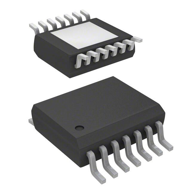
Package
PG-SSOP-14
Marking
TLD1311
Overview
Applications
•
Exterior LED lighting applications such as tail/brake light, turn indicator,
position light, side marker,...
•
Interior LED lighting applications such as ambient lighting, interior
illumination and dash board lighting.
EN
Internal
supply
Thermal
protection
IN_SET
4.7nF**
4.7nF**
4.7nF**
ISO-Pulse
protection circuit
depending on
requirements
VS
CVS =4.7nF
GND
10kΩ
Cmod =2.2µF
VBATT
OUT3
Output
control
Current
adjustment
OUT2
OUT1
DIS
* In case PWM via VS is performed
** For EMI improvement if required
CST =100pF**
ST
470kΩ*
TLD1311EL
GND
Status
CN-1
RSET
N-1
to other LITIX™ Basic
Application Diagram with TLD1311EL
Data Sheet
www.infineon.com
Rev. 1.2
2018-04-26
�LITIX™ Basic
TLD1311EL
Overview
Basic Features
•
3 Channel device with integrated output stages (current sources), optimized to drive LEDs with output
current up to 120 mA per channel
•
Low current consumption in sleep mode
•
PWM-operation supported via VS- and EN-pin
•
Output current adjustable via external low power resistor and possibility to connect PTC resistor for LED
protection during over temperature conditions
•
Reverse polarity protection and overload protection
•
Undervoltage detection
•
N-1 detection, latched function
•
Wide temperature range: -40°C < Tj < 150°C
•
PG-SSOP-14 package with exposed heatslug
Description
The LITIX™ Basic TLD1311EL is a three channel high side driver IC with integrated output stages. It is designed
to control LEDs with a current up to 120 mA. In typical automotive applications the device is capable to drive
i.e. 3 red LEDs per chain (total 9 LEDs) with a current up to 60 mA, which is limited by thermal cooling aspects.
The output current is controlled practically independent of load and supply voltage changes.
Table 1
Product Summary
Parameter
Symbol
Value
Operating voltage range
VS(nom)
5.5 V ... 40 V
Maximum voltage
VS(max)
VOUTx(max)
40 V
Nominal output (load) current
IOUTx(nom)
60 mA when using a supply voltage range of 8 V - 18 V (e.g.
Automotive car battery). Currents up to IOUT(max) possible in
applications with low thermal resistance RthJA
Maximum output (load) current
IOUTx(max)
120 mA; depending on thermal resistance RthJA
Output current accuracy at RSET = 12 kΩ
kLT
750 ± 7%
Current consumption in sleep mode IS(sleep,typ)
0.1 µA
Protective Functions
•
ESD protection
•
Under voltage lock out
•
Over Load protection
•
Over Temperature protection
•
Reverse Polarity protection
Diagnostic Functions
•
N-1 detection, latched function
•
SC to Vs (indicated by N-1 diagnosis)
Data Sheet
2
Rev. 1.2
2018-04-26
�LITIX™ Basic
TLD1311EL
Block Diagram
Block Diagram
VS
2
EN
Internal
supply
Thermal
protection
IN_SET
OUT3
Output
control
Current
adjustment
OUT2
OUT1
DIS
N-1
Figure 1
Data Sheet
GND
TLD1311EL
ST
Status
Basic Block Diagram
3
Rev. 1.2
2018-04-26
�LITIX™ Basic
TLD1311EL
Pin Configuration
3
Pin Configuration
3.1
Pin Assignment
Figure 2
Data Sheet
VS
1
VS
2
EN
3
NC
4
DIS
14
NC
13
OUT3
12
OUT2
11
OUT1
5
10
ST
IN_SET
6
9
GND
N-1
7
8
NC
TLD1311EL
EP
Pin Configuration
4
Rev. 1.2
2018-04-26
�LITIX™ Basic
TLD1311EL
Pin Configuration
3.2
Pin Definitions and Functions
Pin
Symbol
Input/
Output
Function
1, 2
VS
–
Supply Voltage; battery supply, connect a decoupling capacitor (100 nF - 1 µF)
to GND
3
EN
I
Enable pin
4
NC
–
Pin not connected
5
DIS
I
Disable Input
6
IN_SET
I/O
Input / SET pin; Connect a low power resistor to adjust the output current
7
N-1
I/O
N-1 pin
8
NC
–
Pin not connected
–
1)
9
GND
Ground
10
ST
I/O
Status pin
11
OUT1
O
Output 1
12
OUT2
O
Output 2
13
OUT3
O
Output 3
14
NC
–
Pin not connected
–
1)
Exposed
Pad
GND
Exposed Pad; connect to GND in application
1) Connect all GND-pins together.
Data Sheet
5
Rev. 1.2
2018-04-26
�LITIX™ Basic
TLD1311EL
General Product Characteristics
4
General Product Characteristics
4.1
Absolute Maximum Ratings
Absolute Maximum Ratings 1)
Tj = -40°C to +150°C; all voltages with respect to ground, positive current flowing into pin for input pins (I),
positive currents flowing out of the I/O and output pins (O) (unless otherwise specified)
Pos.
Parameter
Symbol
Limit Values
Min.
Max.
Unit
Conditions
Voltages
4.1.1
Supply voltage
VS
-16
40
V
–
4.1.2
Input voltage EN
VEN
-16
40
V
–
4.1.3
Input voltage EN related to VS
VEN(VS)
VS - 40
VS + 16
V
–
4.1.4
Input voltage EN related to VOUTx
VEN - VOUTx
VEN VOUTx
-16
40
V
–
4.1.5
Output voltage
VOUTx
-1
40
V
–
4.1.6
Power stage voltage
VPS = VS - VOUTx
VPS
-16
40
V
–
4.1.7
Input voltage DIS
VDIS
-0.3
6
V
–
4.1.8
IN_SET voltage
VIN_SET
-0.3
6
V
–
4.1.9
N-1 voltage
VN-1
-0.3
6
V
–
4.1.10
Status voltage
VST
-0.3
6
V
–
4.1.11
IN_SET current
IIN_SET
–
–
2
8
mA
–
Diagnosis output
4.1.12
N-1 current
IN-1
-0.5
0.5
mA
–
4.1.13
Output current
IOUTx
–
130
mA
–
Currents
Temperatures
4.1.14
Junction temperature
Tj
-40
150
°C
–
4.1.15
Storage temperature
Tstg
-55
150
°C
–
ESD Susceptibility
4.1.16
ESD resistivity to GND
VESD
-2
2
kV
Human Body
Model (100 pF via
1.5 kΩ)2)
4.1.17
ESD resistivity all pins to GND
VESD
-500
500
V
CDM3)
4.1.18
ESD resistivity corner pins to GND
VESD
-750
750
V
CDM3)
1) Not subject to production test, specified by design
2) ESD susceptibility, Human Body Model “HBM” according to ANSI/ESDA/JEDEC JS-001-2011
3) ESD susceptibility, Charged Device Model “CDM” according to JESD22-C101E
Note: Stresses above the ones listed here may cause permanent damage to the device. Exposure to absolute
maximum rating conditions for extended periods may affect device reliability.
Data Sheet
6
Rev. 1.2
2018-04-26
�LITIX™ Basic
TLD1311EL
General Product Characteristics
Note: Integrated protection functions are designed to prevent IC destruction under fault conditions described in
the data sheet. Fault conditions are considered as “outside” normal operating range. Protection functions
are not designed for continuous repetitive operation.
Functional Range
4.2
Pos.
Parameter
Symbol
Limit Values
Min.
Max.
Unit
Conditions
4.2.19
Supply voltage range for
normal operation
VS(nom)
5.5
40
V
–
4.2.20
Power on reset threshold
VS(POR)
–
5
V
VEN = VS
RSET = 12 kΩ
IOUTx = 80% IOUTx(nom)
VOUTx = 2.5 V
4.2.21
Junction temperature
Tj
-40
150
°C
–
Note: Within the functional range the IC operates as described in the circuit description. The electrical
characteristics are specified within the conditions given in the related electrical characteristics table.
Thermal Resistance
4.3
Pos.
Parameter
Symbol
4.3.1
Junction to Case
RthJC
4.3.2
Junction to Ambient 1s0p board
RthJA1
4.3.3
1)
2)
3)
4)
Junction to Ambient 2s2p board
Limit Values
Min.
Typ.
Max.
–
8
10
–
–
61
56
Unit
Conditions
K/W
1) 2)
K/W
1) 3)
–
–
Ta = 85 °C
Ta = 135 °C
K/W
RthJA2
1) 4)
–
45
–
Ta = 85 °C
–
43
–
Ta = 135 °C
Not subject to production test, specified by design. Based on simulation results.
Specified RthJC value is simulated at natural convection on a cold plate setup (all pins and the exposed Pad
are fixed to ambient temperature). Ta = 85°C, Total power dissipation 1.5 W.
The RthJA values are according to Jedec JESD51-3 at natural convection on 1s0p FR4 board. The product
(chip + package) was simulated on a 76.2 x 114.3 x 1.5 mm3 board with 70 µm Cu, 300 mm2 cooling area.
Total power dissipation 1.5 W distributed statically and homogenously over all power stages.
The RthJA values are according to Jedec JESD51-5,-7 at natural convection on 2s2p FR4 board. The product
(chip + package) was simulated on a 76.2 x 114.3 x 1.5 mm3 board with 2 inner copper layers (outside 2 x
70 µm Cu, inner 2 x 35 µm Cu). Where applicable, a thermal via array under the exposed pad contacted the
first inner copper layer. Total power dissipation 1.5 W distributed statically and homogenously over all
power stages.
Data Sheet
7
Rev. 1.2
2018-04-26
�LITIX™ Basic
TLD1311EL
EN Pin
5
EN Pin
The EN pin is a dual function pin:
Internal Supply
Output Control
EN
V EN
Figure 3
Block Diagram EN pin
Note: The current consumption at the EN-pin IEN needs to be added to the total device current consumption. The
total current consumption is the sum of the currents at the VS-pin IS and the EN-pin IEN.
5.1
EN Function
If the voltage at the pin EN is below a threshold of VEN(off) the LITIX™ Basic IC will enter Sleep mode. In this state
all internal functions are switched off, the current consumption is reduced to IS(sleep). A voltage above VEN(on) at
this pin enables the device after the Power on reset time tPOR.
VS
V EN
IOU T
t
t
tPOR
100%
80%
t
Figure 4
Data Sheet
Power on reset
8
Rev. 1.2
2018-04-26
�LITIX™ Basic
TLD1311EL
EN Pin
5.2
Internal Supply Pin
The EN pin can be used to supply the internal logic. There are two typical application conditions, where this
feature can be used:
1) In “DC/DC control Buck” configurations, where the voltage Vs can be below 5.5V.
2) In configurations, where a PWM signal is applied at the Vbatt pin of a light module. The buffer capacitor CBUF
is used to supply the LITIX™ Basic IC during Vbatt low (Vs low) periods. This feature can be used to minimize
the turn-on time to the values specified in Pos. 10.2.15. Otherwise, the power-on reset delay time tPOR
(Pos. 6.1.8) has to be considered.
The capacitor can be calculated using the following formula:
I EN LS
C BUF = tLOW max -------------------------------------------------V S – V D1 – V S POR
(1)
See also a typical application drawing in Chapter 11.
VBATT
VS
D1
GND
CBUF
EN
Internal
supply
Thermal
protection
Current
adjustment
OUT2
OUT1
LITIX™ Basic
Figure 5
Data Sheet
GND
R SET
IN_SET
OUT3
Output
control
External circuit when applying a fast PWM signal on VBATT
9
Rev. 1.2
2018-04-26
�LITIX™ Basic
TLD1311EL
EN Pin
V EN
t
V BATT
IOU T
t
tON (VS)
100%
80%
Switch off behavior depends on
V BATT and load characteristics
20%
t
Figure 6
Typical waveforms when applying a fast PWM signal on VBATT
The parameter tON(VS) is defined at Pos. 10.2.15. The parameter tOFF(VS) depends on the load and supply voltage
VBATT characteristics.
5.3
EN Unused
In case of an unused EN pin, there are two different ways to connect it:
5.3.1
EN - Pull Up to VS
The EN pin can be connected with a pull up resistor (e.g. 10 kΩ) to Vs potential. In this configuration the
LITIX™ Basic IC is always enabled.
5.3.2
EN - Direct Connection to VS
The EN pin can be connected directly to the VS pin (IC always enabled). This configuration has the advantage
(compared to the configuration described in Chapter 5.3.1) that no additional external component is
required.
Data Sheet
10
Rev. 1.2
2018-04-26
�LITIX™ Basic
TLD1311EL
DIS Pin
6
DIS Pin
The DIS pin is designed as a single function pin.
IDIS(L)
Output Control
DIS
VDIS
Figure 7
Block Diagram DIS pin
The pin can be used for PWM-dimming via a push-pull stage of a micro controller, which is connecting the DISpin to a low or high potential.
Note: The micro controller’s push-pull stage has to be capable to sink currents according to Pos. 6.1.17 to
activate the device.
V D IS
IOU T
tON (D IS)
tOFF(D IS)
t
100%
80%
20%
t
Figure 8
Data Sheet
Turn on and Turn off time for DIS pin usage
11
Rev. 1.2
2018-04-26
�LITIX™ Basic
TLD1311EL
DIS Pin
6.1
Electrical Characteristics Internal Supply / EN / DIS Pin
Electrical Characteristics Internal Supply / EN / DIS pin
Unless otherwise specified: VS = 5.5 V to 40 V, Tj = -40°C to +150°C, RSET = 12 kΩ all voltages with respect to
ground, positive current flowing into pin for input pins (I), positive currents flowing out of the I/O and output
pins (O) (unless otherwise specified)
Pos.
Parameter
Symbol
6.1.1
Current consumption,
sleep mode
IS(sleep)
6.1.2
Current consumption,
active mode
IS(on)
Limit Values
Min.
Typ.
Max.
–
0.1
2
–
–
–
6.1.3
Current consumption,
device disabled via ST
–
–
–
6.1.4
–
–
–
6.1.5
Current consumption,
device disabled via DIS
–
–
–
Data Sheet
–
–
–
12
1)
VEN = 0.5 V
Tj < 85 °C
VS = 18 V
VOUTx = 3.6 V
mA
2)
IIN_SET = 0 µA
Tj < 105 °C
VS = 18 V
VOUTx = 3.6V
VEN = 5.5 V
VEN = 18 V
1)
REN = 10 kΩ between
VS and EN-pin
mA
2)
VS = 18 V
Tj < 105 °C
VST = 5 V
VEN = 5.5 V
VEN = 18 V
1)
REN = 10 kΩ between
VS and EN-pin
mA
2)
VS = 18 V
Tj < 105 °C
VIN_SET = 5 V
VEN = 5.5 V
VEN = 18 V
1)
REN = 10 kΩ between
VS and EN-pin
mA
2)
1.4
0.7
1.4
IS(dis,DIS)
–
–
–
µA
1.4
0.65
1.4
Current consumption,
IS(dis,IN_SET)
device disabled via IN_SET
–
–
–
Conditions
1.4
0.75
1.5
IS(dis,ST)
–
–
–
Unit
1.6
0.75
1.6
VS = 18 V
Tj < 105 °C
VDIS= 3.4 V
VEN = 5.5 V
VEN = 18 V
1)
REN = 10 kΩ between
VS and EN-pin
Rev. 1.2
2018-04-26
�LITIX™ Basic
TLD1311EL
DIS Pin
Electrical Characteristics Internal Supply / EN / DIS pin (cont’d)
Unless otherwise specified: VS = 5.5 V to 40 V, Tj = -40°C to +150°C, RSET = 12 kΩ all voltages with respect to
ground, positive current flowing into pin for input pins (I), positive currents flowing out of the I/O and output
pins (O) (unless otherwise specified)
Pos.
Parameter
Symbol
Limit Values
Min.
6.1.6
–
–
–
Conditions
mA
2)
VS = 18 V
Tj < 105 °C
RSET = 12 kΩ
VDIS= 0.5 V
VOUTx = 18 V
VEN = 5.5 V
VEN = 18 V
1)
REN = 10 kΩ between
VS and EN-pin
mA
2)
VS = 18 V
Tj < 105 °C
RSET = 12 kΩ
VDIS= 0.5 V
VOUTx = 18 V
VST = 0 V
VEN = 5.5 V
VEN = 18 V
1)
REN = 10 kΩ between
VS and EN-pin
1)
Max.
Current consumption,
IS(fault,STu)
active mode in single fault
detection condition with
ST-pin unconnected
–
–
–
6.1.7
Typ.
Unit
1.7
1.1
1.8
Current consumption,
IS(fault,STG)
active mode in single fault
detection condition with
ST-pin connected to GND
–
–
–
–
–
–
6.0
4.9
5.9
Power-on reset delay time tPOR
–
–
25
µs
VS = VEN = 0 →13.5 V
VOUTx(nom) = 3.6 ± 0.3V
IOUTx = 80% IOUTx(nom)
6.1.9
Required supply voltage
for output activation
VS(on)
–
–
4
V
VEN = 5.5 V
VOUTx = 3 V
IOUTx = 50% IOUTx(nom)
6.1.10
Required supply voltage
for current control
VS(CC)
–
–
5.2
V
VEN = 5.5 V
VOUTx = 3.6 V
IOUTx ≥ 90% IOUTx(nom)
6.1.11
EN turn on threshold
VEN(on)
–
–
2.5
V
–
6.1.12
EN turn off threshold
VEN(off)
0.8
–
–
V
–
mA
1)
VS = 4.5 V
Tj < 105 °C
VEN = 5.5 V
mA
Tj < 105 °C
VS = 13.5 V, VEN = 5.5 V
VS = 18 V, VEN = 5.5 V
VS = VEN = 18 V
1)
VS = 18 V, REN = 10 kΩ
between VS and EN-pin
6.1.8
3)
6.1.13
EN input current during
low supply voltage
IEN(LS)
6.1.14
EN high input current
IEN(H)
Data Sheet
–
–
–
–
–
–
–
–
–
–
13
1.8
0.1
0.1
1.65
0.45
Rev. 1.2
2018-04-26
�LITIX™ Basic
TLD1311EL
DIS Pin
Electrical Characteristics Internal Supply / EN / DIS pin (cont’d)
Unless otherwise specified: VS = 5.5 V to 40 V, Tj = -40°C to +150°C, RSET = 12 kΩ all voltages with respect to
ground, positive current flowing into pin for input pins (I), positive currents flowing out of the I/O and output
pins (O) (unless otherwise specified)
Pos.
Parameter
Symbol
Limit Values
Min.
Typ.
Max.
Unit
Conditions
6.1.15
DIS (active low)
Switching low threshold
(outputs on)
VDIS(L)
1.5
–
–
V
1)
6.1.16
DIS (active low)
Switching high threshold
(outputs off)
VDIS(H)
–
–
3.2
V
1)4)
6.1.17
DIS(active low)
Low input current with
active channels (voltage
8 V
Tj = 25...150 °C
VS = VOUTx (OL) x
Rev. 1.2
2018-04-26
�LITIX™ Basic
TLD1311EL
Load Diagnosis
Electrical Characteristics IN_SET pin and Load Diagnosis (cont’d)
Unless otherwise specified: VS = 5.5 V to 40 V, Tj = -40°C to +150°C, RSET = 12 kΩ, all voltages with respect to ground,
positive current flowing into pin for input pins (I), positive currents flowing out of the I/O and output pins (O) (unless
otherwise specified)
Pos.
Parameter
Symbol
IIN_SET(N-1)
Limit Values
Unit
Conditions
7.4
mA
1)
VS > 8 V
Tj = 25...150 °C
VIN_SET = 4 V
VS = VOUTx (OL)
Min.
Typ.
Max.
1.5
–
9.3.3
IN_SET N_1 current
9.3.4
ST device turn on
VST(L)
threshold (active low) in
case of voltage applied
from external (ST-pin
acting as input)
0.8
–
–
V
–
9.3.5
VST(H)
ST device turn off
threshold (active low) in
case of voltage applied
from external (ST-pin
acting as input)
–
–
2.5
V
–
9.3.6
ST pull down current
IST(PD)
–
–
15
µA
VEN = 5.5 V
VST = 0.8 V
9.3.7
ST N_1 voltage (ST-pin
acting as diagnosis
output)
VST(N-1)
4
–
5.5
V
1)
VS > 8 V
Tj = 25...150 °C
RST = 470 kΩ
VS = VOUTx (OL)
9.3.8
ST N_1 current (ST-pin
acting as diagnosis
output)
IST(N-1)
100
–
220
µA
1)
VS > 8 V
Tj = 25...150 °C
VST = 2.5 V
VS = VOUTx (OL)
9.3.9
N-1 high threshold
VN-1(th)
2.45
2.85
3.2
V
VS > 8 V
9.3.10
N-1 output current
IN-1
12
20
28
µA
VS > 8 V
VN-1 = 2 V
9.3.11
N-1 detection voltage
VPS(N-1) = VS - VOUTx
VPS(N-1)
0.2
–
0.4
V
VS > 8 V
–
15
µA
See Figure 13
2
IN_SET activation
IIN_SET(act)
current without turn on
of output stages
1) Not subject to production test, specified by design
9.3.12
Data Sheet
24
Rev. 1.2
2018-04-26
�LITIX™ Basic
TLD1311EL
Power Stage
10
Power Stage
The output stages are realized as high side current sources with a current of 120 mA. During off state the
leakage current at the output stage is minimized in order to prevent a slightly glowing LED.
The maximum current of each channel is limited by the power dissipation and used PCB cooling areas (which
results in the applications RthJA).
For an operating current control loop the supply and output voltages according to the following parameters
have to be considered:
•
•
•
Required supply voltage for current control VS(CC), Pos. 6.1.10
Voltage drop over output stage during current control VPS(CC), Pos. 10.2.6
Required output voltage for current control VOUTx(CC), Pos. 10.2.7
10.1
Protection
The device provides embedded protective functions, which are designed to prevent IC destruction under fault
conditions described in this data sheet. Fault conditions are considered as “outside” normal operating range.
Protective functions are neither designed for continuous nor for repetitive operation.
10.1.1
Over Load Behavior
An over load detection circuit is integrated in the LITIX™ Basic IC. It is realized by a temperature monitoring of
the output stages (OUTx).
As soon as the junction temperature exceeds the current reduction temperature threshold Tj(CRT) the output
current will be reduced by the device by reducing the IN_SET reference voltage VIN_SET(ref). This feature avoids
LED’s flickering during static output overload conditions. Furthermore, it protects LEDs against over
temperature, which are mounted thermally close to the device. If the device temperature still increases, the
three output currents decrease close to 0 A. As soon as the device cools down the output currents rise again.
IOU T
V IN_ SET
Tj (C R T)
Figure 20
Tj
Output current reduction at high temperature
Note: This high temperature output current reduction is realized by reducing the IN_SET reference voltage
voltage (Pos. 9.3.1). In case of very high power loss applied to the device and very high junction
temperature the output current may drop down to IOUTx = 0 mA, after a slight cooling down the current
increases again.
10.1.2
Reverse Battery Protection
The TLD1311EL has an integrated reverse battery protection feature. This feature protects the driver IC itself,
but also connected LEDs. The output reverse current is limited to IOUTx(rev) by the reverse battery protection.
Data Sheet
25
Rev. 1.2
2018-04-26
�LITIX™ Basic
TLD1311EL
Power Stage
Note: Due to the reverse battery protection a reverse protection diode for the light module may be obsolete. In
case of high ISO-pulse requirements and only minor protecting components like capacitors a reverse
protection diode may be reasonable. The external protection circuit needs to be verified in the application.
10.2
Electrical Characteristics Power Stage
Electrical Characteristics Power Stage
Unless otherwise specified: VS = 5.5 V to 18 V, Tj = -40°C to +150°C, VOUTx = 3.6 V, all voltages with respect to
ground, positive current flowing into pin for input pins (I), positive currents flowing out of the I/O and output
pins (O) (unless otherwise specified)
Pos.
Parameter
Symbol
Limit Values
Min.
10.2.1
Output leakage current
Typ.
Unit
Conditions
µA
VEN = 5.5 V
IIN_SET = 0 µA
VOUTx = 2.5 V
Tj = 150 °C
1)
Tj = 85 °C
1)
Max.
IOUTx(leak)
–
–
–
–
7
3
10.2.2
Output leakage current in
boost over battery setup
–
IOUTx(leak,B2B)
–
50
µA
10.2.3
Reverse output current
-IOUTx(rev)
–
1
µA
10.2.4
Output current accuracy
kLT
limited temperature range
–
Output current accuracy
over temperature
1)
VS = -16 V
Output load: LED with
break down voltage
< - 0.6 V
1)
697
645
10.2.5
VEN = 5.5 V
IIN_SET = 0 µA
VOUTx = VS = 40 V
750
750
Tj = 25...115 °C
VS = 8...18 V
VPS = 2 V
RSET = 6...12 kΩ
RSET = 30 kΩ
803
855
1)
kALL
697
645
750
750
803
855
Tj = -40...115 °C
VS = 8...18 V
VPS = 2 V
RSET = 6...12 kΩ
RSET = 30 kΩ
10.2.6
Voltage drop over power
stage during current
control VPS(CC) = VS - VOUTx
VPS(CC)
0.75
–
–
V
1)
10.2.7
Required output voltage
for current control
VOUTx(CC)
2.3
–
–
V
1)
Data Sheet
26
VS = 13.5 V
RSET = 12 kΩ
IOUTx ≥ 90% of
(kLT(typ)/RSET)
VS = 13.5 V
RSET = 12 kΩ
IOUTx ≥ 90% of
(kLT(typ)/RSET)
Rev. 1.2
2018-04-26
�LITIX™ Basic
TLD1311EL
Power Stage
Electrical Characteristics Power Stage (cont’d)
Unless otherwise specified: VS = 5.5 V to 18 V, Tj = -40°C to +150°C, VOUTx = 3.6 V, all voltages with respect to
ground, positive current flowing into pin for input pins (I), positive currents flowing out of the I/O and output
pins (O) (unless otherwise specified)
Pos.
Parameter
Symbol
Limit Values
Min.
Typ.
Max.
Unit
Conditions
10.2.8
Maximum output current
IOUT(max)
120
–
–
mA
RSET = 4.7 kΩ
The maximum output
current is limited by the
thermal conditions.
Please refer to
Pos. 4.3.1 - Pos. 4.3.3
10.2.9
DIS turn on time
tON(DIS)
–
–
15
µs
2)
VS = 13.5 V
RSET = 12 kΩ
DIS → L
IOUTx = 80% of
(kLT(typ)/RSET)
10.2.10 DIS turn off time
tOFF(DIS)
–
–
10
µs
2)
VS = 13.5 V
RSET = 12 kΩ
DIS → H
IOUTx = 20% of
(kLT(typ)/RSET)
10.2.11 ST turn on time
tON(ST)
–
–
15
µs
3)
10.2.12 ST turn off time
tOFF(ST)
–
–
10
µs
VS = 13.5 V
RSET = 12 kΩ
ST →H
IOUTx = 20% of
(kLT(typ)/RSET)
10.2.13 IN_SET turn on time
tON(IN_SET)
–
–
15
µs
VS = 13.5 V
IIN_SET = 0 → 100 µA
IOUTx = 80% of
(kLT(typ)/RSET)
10.2.14 IN_SET turn off time
tOFF(IN_SET)
–
–
10
µs
VS = 13.5 V
IIN_SET = 100 → 0 µA
IOUTx = 20% of
(kLT(typ)/RSET)
10.2.15 VS turn on time
tON(VS)
–
–
20
µs
1) 4)
Data Sheet
27
VS = 13.5 V
RSET = 12 kΩ
ST → L
IOUTx = 80% of
(kLT(typ)/RSET)
3)
VEN = 5.5 V
RSET = 12 kΩ
VS = 0 → 13.5 V
IOUTx = 80% of
(kLT(typ)/RSET)
Rev. 1.2
2018-04-26
�LITIX™ Basic
TLD1311EL
Power Stage
Electrical Characteristics Power Stage (cont’d)
Unless otherwise specified: VS = 5.5 V to 18 V, Tj = -40°C to +150°C, VOUTx = 3.6 V, all voltages with respect to
ground, positive current flowing into pin for input pins (I), positive currents flowing out of the I/O and output
pins (O) (unless otherwise specified)
Pos.
Parameter
10.2.16 Current reduction
temperature threshold
Symbol
Tj(CRT)
Limit Values
Conditions
1)
Min.
Typ.
Max.
–
140
–
°C
IOUTx = 95% of
(kLT(typ)/RSET)
–
A
1)
10.2.17 Output current during
IOUT(CRT)
85% of –
current reduction at high
(kLT(typ)
temperature
/RSET)
1) Not subject to production test, specified by design
2) see also Figure 8
3) see also Figure 16
4) see also Figure 6
Data Sheet
Unit
28
RSET = 12 kΩ
Tj = 150 °C
Rev. 1.2
2018-04-26
�LITIX™ Basic
TLD1311EL
Application Information
11
Application Information
Note: The following information is given as a hint for the implementation of the device only and shall not be
regarded as a description or warranty of a certain functionality, condition or quality of the device.
Vbat
BCM
PROFET
VBB
channel1
load current
sens e
internal
power
supply
logic
open load
detection
IN1
ESD
protectio n
IS1
clamp for
inductive load
gate control
&
charge pump
multi step
load current
limitation
OU T1
temperature
sens or
SEN
channel2
control and protection circ uit
equivale nt to
channel 1
IN2
IS2
OU T2
R GND
GN D
VBATT
Cmod =2.2 µF
CVS =4.7nF
ISO- Pulse
protection circuit
depending on
requirements
CVS =4.7nF
VS
10k
EN
Output
control
4.7nF** 4.7nF** 4.7nF**
OUT2
adjust
R SET
LITIX™ Basic
GND
RSET
Thermal
protection
Status
GND
4.7nF** 4.7nF** 4.7nF**
OUT3
OUT2
N-1
CN-1
ST
Output
control
DIS
OUT1
IN_SET Current
LITIX™ Basic
Internal
supply
4.7nF** 4.7nF** 4.7nF**
OUT3
OUT2
adjust
Status
ST
Output
control
N-1
CN-1
IN_ SET Current
EN
DIS
OUT1
N-1
C N-1
Thermal
protection
OUT3
DIS
VS
10k
Internal
supply
EN
Thermal
protection
CVS =4.7nF
VS
10k
Internal
supply
RSET
IN_ SET
OUT1
Current
adjust
LITIX™ Basic
VZD >VOUT(CC)
Status
ST
GND
R


 工商网监
湘ICP备2023018690号
工商网监
湘ICP备2023018690号
