5-V Low Drop Voltage Regulator
TLE 4290
Features
•
•
•
•
•
•
•
•
•
•
^
Output voltage 5 V ± 2%
Very low current consumption
450 mA current capability
Power Good Feature
Very low-drop voltage
Short-circuit-proof
Reverse polarity proof
Suitable for use in automotive electronics
Green Product (RoHS compliant)
AEC Qualified
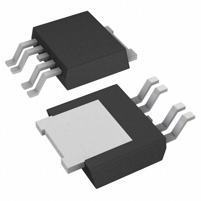
P-TO252-5-11
Functional Description
The TLE 4290 is a monolithic integrated low drop voltage
regulator which can supply loads up to 450 mA with
power good feature. An input voltage up to 42 V is
P-TO263-5-1
regulated to VQ,nom = 5.0 V. The device is designed to
supply μ-controllers in the severe environment of
automotive applications. Therefore it is protected against
overload, short circuit and over temperature conditions. Of course the TLE 4290 can
been used also in all other applications, where a stabilized 5 V voltage is required.
Type
Package
TLE 4290 D
PG-TO252-5-11
TLE 4290 G
PG-TO263-5-1
Data Sheet
1
Rev. 1.7, 2007-03-20
�TLE 4290
Power Good
The Power Good PG pin informs e.g. the microcontroller in case the output voltage has
fallen below the lower threshold VQ,pgt-d of typ. 3.65 V. Connecting the regulator to a
battery voltage at first the power good signal remains LOW. When the output voltage has
reached the higher threshold VQ,pgt-i the power good output remains still LOW for the
power good delay time trd. Afterwards the power good output turns HIGH. The delay time
can be set by the user with an external capacitor at pin D according to the requirements
of the application.
The Power Good circuitry supervises the output voltage. In case VQ falls below the lower
Power Good switching threshold VQ,pgt-d the PG output is set LOW after the Power Good
reaction time. The Power Good LOW signal is generated down to an output voltage VQ
to 1 V. A LOW signal at the Power Good pin informs that the battery was lost and
memory is no longer valid.
The feature should be used in combination with a microcontroller with internal reset.
TLE 4290
I
1
5
Q
Current
and
Saturation
Control
BandGapReference
2
Power
Good
Control
PG
4
GND
Figure 1
Data Sheet
D
AEB02823
Block Diagram
2
Rev. 1.7, 2007-03-20
�TLE 4290
PG-TO263-5-1
PG-TO252-5-11
GND
I PG
D Q
AEP02825
I
PG GND D
Q
AEP02827
Figure 2
Pin Configuration (top view)
Table 1
Pin Definitions and Functions
Pin No.
Symbol
Function
1
I
Input; block to ground directly at the IC with a ceramic capacitor.
2
PG
Power Good; open collector output.
Add a pull-up resistor of > 5 kΩ to pin Q.
3
GND
Ground; Pin 3 internally connected to heatsink.
4
D
Delay; connect a capacitor to GND for setting power good delay
time.
5
Q
Output; block to ground with a capacitor, C ≥ 22 μF
ESR < 5 Ω at 10 kHz.
Data Sheet
3
Rev. 1.7, 2007-03-20
�TLE 4290
Table 2
Absolute Maximum Ratings
Parameter
Symbol
Limit Values
Unit Test Condition
Min.
Max.
VI
II
-42
45
V
–
–
–
–
Internally limited
VQ
IQ
-1.0
16
V
–
–
–
–
Internally limited
VPG
IPG
-0.3
25
V
–
-5
5
mA
–
VD
ID
-0.3
7
V
–
-2
2
mA
–
Tj
Tstg
-40
150
°C
–
-50
150
°C
–
Input I
Voltage
Current
Output Q
Voltage
Current
Power Good Output PG
Voltage
Current
Delay D
Voltage
Current
Temperature
Junction temperature
Storage temperature
Note: Stresses above those listed here may cause permanent damage to the device.
Exposure to absolute maximum rating conditions for extended periods may affect
device reliability.
Data Sheet
4
Rev. 1.7, 2007-03-20
�TLE 4290
Table 3
Operating Range
Parameter
Input voltage
Junction temperature
Symbol
Limit Values
Unit
Remarks
Min.
Max.
VI
Tj
5.5
42
V
–
-40
150
°C
–
Rthj-c
Rthj-a
Rthj-a
–
4
K/W
–
–
53
K/W
TO2631)
–
78
K/W
TO2521)
Thermal Resistance
Junction case
Junction ambient
Junction ambient
1) Worst case, regarding peak temperature; zero airflow; mounted on a PCB FR4, 80 × 80 × 1.5 mm3, heat sink
area 300 mm2
Note: In the operating range, the functions given in the circuit description are fulfilled.
Data Sheet
5
Rev. 1.7, 2007-03-20
�TLE 4290
Table 4
Characteristics
VI = 13.5 V; -40 °C < Tj < 150 °C (unless otherwise specified)
Parameter
Symbol
Limit Values
Min.
Typ. Max.
Unit
Measuring
Condition
Output
Output voltage
VQ
4.9
5.0
5.1
V
5 mA < IQ < 400 mA;
6 V < VI < 28 V
Output voltage
VQ
4.9
5.0
5.1
V
5 mA < IQ < 200 mA;
6 V < VI < 40 V
Output current limitation
IQ
Iq
450
700
–
mA
1)
–
200
230
μA
Current consumption;
Iq = II - IQ
Iq
–
200
255
μA
Current consumption;
Iq = II - IQ
Iq
–
5
12
mA
IQ = 1 mA;
Tj = 25 °C
IQ = 1 mA;
Tj ≤ 85 °C
IQ = 250 mA
Current consumption;
Iq
–
12
25
mA
IQ = 400 mA
Drop voltage
Vdr
–
250
500
mV
Load regulation
ΔVQ,lo
-30
15
30
mV
Line regulation
ΔVQ,li
-15
5
15
mV
Power supply ripple
rejection
PSRR
–
60
–
dB
IQ = 300 mA
Vdr = VI - VQ1)
VI = 6 V;
IQ = 5 mA to 400 mA
Vl = 8 V to 32 V;
IQ = 5 mA
fr = 100 Hz;
Vr = 0.5 Vpp
Temperature output
voltage drift
dVQ/dT
–
0.5
–
mV/K –
Output Capacitor
CQ
22
–
–
μF
ESR < 5 Ω in the
operation range
Current consumption;
Iq = II - IQ
Iq = II - IQ
Power Good Output PG and Delay Timing D
Power Good switching
threshold
VQ,pgt-i
4.45
4.65
4.80
V
VQ increasing
Power Good switching
threshold
VQ,pgt-d
3.50
3.65
3.80
V
VQ decreasing
Data Sheet
6
Rev. 1.7, 2007-03-20
�TLE 4290
Table 4
Characteristics (cont’d)
VI = 13.5 V; -40 °C < Tj < 150 °C (unless otherwise specified)
Parameter
Symbol
Limit Values
Min.
Typ. Max.
Unit
Measuring
Condition
Power Good output low
voltage
VPGL
–
0.2
0.4
V
Power Good output
leakage current
IPGH
–
0
2
μA
RPG ≥ 5 kΩ;
VQ > 1 V
VPG > 4.5 V
Power Good charging
current
ID,c
3
6
9
μA
VD = 1 V
1.5
1.8
2.2
V
–
0.60
0.85
1.10
V
–
10
16
22
ms
0.2
0.5
2.0
μs
CD = 47 nF
CD = 47 nF
VDU
Lower timing threshold
VDL
trd
Power Good delay time
Power Good reaction time trr
Upper timing threshold
1) Measured when the output voltage VQ has dropped 100 mV from the nominal value obtained at VI = 13.5 V.
Note: The listed characteristics are ensured over the operating range of the integrated
circuit. Typical characteristics specify mean values expected over the production
spread. If not otherwise specified, typical characteristics apply at Ta = 25 °C and
the given supply voltage.
II
VI
I
CI1
CI2
1000 µF
100 nF
1
5
IQ
Q
CQ
22 µF
RPG
TLE 4290
ID
CD
ID,C
5k
VQ
D
4
2
GND
47 nF
PG
VPG
IGND
AES02824
Figure 3
Data Sheet
Test Circuit
7
Rev. 1.7, 2007-03-20
�TLE 4290
Application Information
CQ1 CQ2
TLE 4290
VBAT
CI1
I 1
5 Q
22
µF
100
nF
µ-Controller
VCC
CI2
BandGapReference
Current
and
Saturation
Control
RPG
5k
2
Power
Good
Control
PG
Internal
Reset
NMI /
PORT
4
GND
D
CD
47 nF
AES02822
Figure 4
Application Diagram
Input, Output
An input capacitor is necessary for damping line influences. A resistor of approx. 1 Ω in
series with CI, can damp the LC of the input inductivity and the input capacitor.
The TLE 4290 requires an output capacitor of at least 22 μF with an ESR below 5 Ω for
stability.
Power Good
The Power Good pin informs e.g. the micro-controller in case the output voltage has
fallen below a threshold of typ. 3.65 V. When the battery voltage is supplied the Power
Good signal indicates a loss of memory due to missing power. After the Memory Good
switching threshold is reached the Power Good output remains low for the Power Good
delay time. This time can be set by the user with an external capacitor at pin D according
to the requirements of the application, e.g. the time until the microcontroller is initialized
and ready to receive any information.
Data Sheet
8
Rev. 1.7, 2007-03-20
�TLE 4290
The power good circuit supervises the output voltage. In case VQ falls below the Power
Good switching threshold the Power Good output PG is set LOW after the power good
reaction time. The power good LOW signal is generated down to an output voltage VQ
to 1 V. A LOW signal at the power good pin informs that the battery was lost and memory
is no longer valid.
The feature should only be used in combination to a microcontroller with internal reset.
For the power good delay time after the output voltage of the regulator is above the reset
threshold, the reset signal is set High again. The reset delay time is defined by the reset
delay capacitor CD at pin D.
The Power Good delay time is defined by the charging time of an external delay
capacitor CD.
CD = (trd × ID,c) / ΔV
(1)
With:
CD = Power Good delay capacitor
trd = Power Good delay time
ΔV = VDU, typical 1.8 V
ID,c = Charge current typical 6 μA
•
•
•
•
VΙ
< t rr
VQ
V Q,pgt_i
V Q,pgt_d
d V Ι D, c
=
dt
CD
VD
VDU
V DL
t rd
t rr
V PG
Power-on
Power Good
Signal
Figure 5
Data Sheet
Thermal
Shutdown
Voltage Dip
at Input
Undervoltage
Secondary
Spike
Overload
at Output
AED03074
Power Good Timing
9
Rev. 1.7, 2007-03-20
�TLE 4290
The power good reaction time trr is the time it takes the voltage regulator to set power
good output PG LOW after the output voltage has dropped below the power good
switching threshold. It is typically 0.5 μs for delay capacitor of 47 nF. For other values for
CD the reaction time can be estimated using the following equation:
trr = 10 ns/nF × CD
(2)
The Power Good output is an open collector output. It requires externally a pull-up
resistor of at least 5 kΩ to Q.
Data Sheet
10
Rev. 1.7, 2007-03-20
�TLE 4290
Typical Performance Characteristics
Output Voltage VQ versus
Temperature Tj
VQ
Output Voltage VQ versus
Input Voltage VI
AED03033
5.2
V
AED01929
12
VQ
V
10
5.1
VI = 13.5 V
5.0
8
4.9
6
4.8
4
4.7
2
4.6
-40
0
40
80
0
120 ˚C 160
Tj
Data Sheet
11
R L = 25 Ω
0
2
4
6
8 V 10
VΙ
Rev. 1.7, 2007-03-20
�TLE 4290
Output Current IQ versus
Temperature Tj
IQ
Output Current IQ versus
Input Voltage VI
AED03034
1200
mA
AED03046
1.2
IQ
A
1000
1.0
800
0.8
600
0.6
400
0.4
T j = 125 ˚C
25 ˚C
200
0.2
0
-40
0
40
80
0
120 ˚C 160
0
10
20
30
40 V 50
Tj
VI
Current Consumption Iq versus
Output Current IQ; Tj = 25 °C
Current Consumption Iq versus
Output Current IQ
AED03112
2.4
Ιq
Ι q mA
AED03035
80
mA
70
2.0
60
1.6
50
1.2
40
VΙ = 13.5 V
30
0.8
VΙ = 13.5 V
20
0.4
10
0
0
20
40
60
80
0
mA 120
ΙQ
Data Sheet
0
100
200
300
400
mA 600
ΙQ
12
Rev. 1.7, 2007-03-20
�TLE 4290
Drop Voltage Vdr versus
Output Current IQ
Vdr
Charge Current ID,c versus
Temperature Tj
AED01935
800
mV
700
AED03036
8
µA
ID, c
7
6
600
500
5
T j = 125 ˚C
25 ˚C
400
4
300
3
200
2
100
1
0
0
200
400
600
mA
0
-40
1000
VI = 13.5 V
VD = 1 V
0
40
80
120 ˚C 160
Tj
IQ
Upper Timing Threshold VDU versus
Temperature Tj
V DU
AED03037
4.0
mA
3.5
3.0
2.5
VΙ = 13.5 V
2.0
1.5
1.0
0.5
0
-40
0
40
80
120 ˚C 160
Tj
Data Sheet
13
Rev. 1.7, 2007-03-20
�TLE 4290
Package Outlines
6.5 +0.15
-0.05
A
1)
2.3 +0.05
-0.10
B
(5)
0.51 MIN.
0.15 MAX.
per side
5 x 0.6 ±0.1
1.14
4.56
0.5 +0.08
-0.04
0.9 +0.20
-0.01
0...0.15
0.8 ±0.15
(4.24) 1 ±0.1
9.98 ±0.5
6.22 -0.2
5.7 MAX.
0.5 +0.08
-0.04
0.1 B
0.25 M A B
1) Includes mold flashes on each side.
All metal surfaces tin plated, except area of cut.
GPT09527
Figure 6
PG-TO252-5-11 (Plastic Transistor Single Outline)
Green Product (RoHS compliant)
To meet the world-wide customer requirements for environmentally friendly products
and to be compliant with government regulations the device is available as a green
product. Green products are RoHS-Compliant (i.e Pb-free finish on leads and suitable
for Pb-free soldering according to IPC/JEDEC J-STD-020).
You can find all of our packages, sorts of packing and others in our
Infineon Internet Page “Products”: http://www.infineon.com/products.
Dimensions in mm
SMD = Surface Mounted Device
Data Sheet
14
Rev. 1.7, 2007-03-20
�TLE 4290
4.4
10 ±0.2
1.27 ±0.1
A
8.5 1)
B
0.05
2.4
0.1
2.7 ±0.3
4.7 ±0.5
7.55 1)
9.25 ±0.2
(15)
1±0.3
0...0.3
0...0.15
5 x 0.8 ±0.1
0.5 ±0.1
4 x 1.7
0.25
M
A B
8˚ MAX.
1) Typical
Metal surface min. X = 7.25, Y = 6.9
All metal surfaces tin plated, except area of cut.
0.1 B
GPT09113
GPT09113
Figure 7
PG-TO263-5-1 (Plastic Transistor Single Outline)
Green Product (RoHS compliant)
To meet the world-wide customer requirements for environmentally friendly products
and to be compliant with government regulations the device is available as a green
product. Green products are RoHS-Compliant (i.e Pb-free finish on leads and suitable
for Pb-free soldering according to IPC/JEDEC J-STD-020).
You can find all of our packages, sorts of packing and others in our
Infineon Internet Page “Products”: http://www.infineon.com/products.
Dimensions in mm
SMD = Surface Mounted Device
Data Sheet
15
Rev. 1.7, 2007-03-20
�TLE 4290
Revision History
Version
Date
Rev. 1.7
2007-03-20 Initial version of RoHS-compliant derivate of TLE 4290
Page 1: AEC certified statement added
Page 1 and Page 14: RoHS compliance statement and
Green product feature added
Page 1 and Page 14: Package changed to RoHS compliant
version
Legal Disclaimer updated
Data Sheet
Changes
16
Rev. 1.7, 2007-03-20
�Edition 2007-03-20
Published by
Infineon Technologies AG
81726 Munich, Germany
© 2007 Infineon Technologies AG
All Rights Reserved.
Legal Disclaimer
The information given in this document shall in no event be regarded as a guarantee of conditions or
characteristics. With respect to any examples or hints given herein, any typical values stated herein and/or any
information regarding the application of the device, Infineon Technologies hereby disclaims any and all warranties
and liabilities of any kind, including without limitation, warranties of non-infringement of intellectual property rights
of any third party.
Information
For further information on technology, delivery terms and conditions and prices, please contact the nearest
Infineon Technologies Office (www.infineon.com).
Warnings
Due to technical requirements, components may contain dangerous substances. For information on the types in
question, please contact the nearest Infineon Technologies Office.
Infineon Technologies components may be used in life-support devices or systems only with the express written
approval of Infineon Technologies, if a failure of such components can reasonably be expected to cause the failure
of that life-support device or system or to affect the safety or effectiveness of that device or system. Life support
devices or systems are intended to be implanted in the human body or to support and/or maintain and sustain
and/or protect human life. If they fail, it is reasonable to assume that the health of the user or other persons may
be endangered.
�


 工商网监
湘ICP备2023018690号
工商网监
湘ICP备2023018690号
