TLE9562-3QX
DC Motor System IC
1
Overview
Features
•
Low-drop voltage regulator 5 V, 250 mA for main supply
•
Four half-bridge gate drivers for external N-channel MOSFETs
•
Adaptive MOSFET gate control:
– Regulation of the MOSFET switching time
– Reduced switching losses in PWM mode
– High efficient constant gate charge
•
Control of reverse battery protection MOSFET
•
High-speed CAN transceiver supporting CAN FD communication up to 5 Mbit/s according to ISO118982:2016 including selective wake-up functionality via CAN partial networking and CAN FD tolerant mode
•
LIN Transceivers LIN2.2/SAE J2602 with programmable TXD time-out feature and LIN flash mode
•
Fail Outputs for fail-safe signalization
•
Configurable wake-up sources
•
Four high-side outputs 7 Ω typ.
•
Two PWM inputs
– High-side and low-side PWM capable
– Active free-wheeling
– Up to 25 kHz PWM frequency
•
32 bit serial peripheral interface (SPI) with cyclic redundancy check (CRC)
•
Very low quiescent current consumption in Stop Mode and Sleep Mode
•
Periodic cyclic sense and cyclic wake in Normal Mode, Stop Mode and Sleep Mode
•
Reset and interrupt output
•
Drain-source monitoring and open-load detection
•
Configurable time-out and window watchdog
•
Overtemperature and short circuit protection features
•
Leadless power package with support of optical lead tip inspection
•
Green Product (RoHS compliant)
Datasheet
www.infineon.com
1
Rev. 1.0
2021-01-21
�TLE9562-3QX
DC Motor System IC
Overview
Potential applications
•
Door module
•
Power lift gate
•
Power sliding doors
•
Seat control module
•
Seatbelt pretension
•
Steering column lock
•
Sunroof module
Product validation
Qualified for automotive applications. Product validation according to AEC-Q100.
Description
The TLE9562-3QX is a multifunctional system IC with integrated power supply, communication interfaces,
multiple half-bridges and support features in an exposed pad PG-VQFN-48 power package. The device is
designed for various motor control automotive applications.
To support these applications, the DC Motor System IC provides the main functions, such as a 5 V low-dropout
voltage regulator one HS-CAN transceiver supporting CAN FD, CAN Partial Networking (incl. FD tolerant
mode), one LIN transceiver, four half-bridges for DC motor control, and one 32 bit serial peripheral interface
(SPI).
The device includes diagnostic and supervision features, such as drain-source monitoring and open-load
detection, short circuit protection, configurable time-out and window watchdog, fail-safe output, as well as
overtemperature protection.
Type
Package
Marking
TLE9562-3QX
PG-VQFN-48
TLE9562-3QX
Datasheet
2
Rev. 1.0
2021-01-21
�TLE9562-3QX
DC Motor System IC
Table of Contents
1
Overview . . . . . . . . . . . . . . . . . . . . . . . . . . . . . . . . . . . . . . . . . . . . . . . . . . . . . . . . . . . . . . . . . . . . . . . 1
2
Block Diagram . . . . . . . . . . . . . . . . . . . . . . . . . . . . . . . . . . . . . . . . . . . . . . . . . . . . . . . . . . . . . . . . . . . 8
3
3.1
3.2
3.3
Pin Configuration . . . . . . . . . . . . . . . . . . . . . . . . . . . . . . . . . . . . . . . . . . . . . . . . . . . . . . . . . . . . . . . . . 9
Pin Assignment . . . . . . . . . . . . . . . . . . . . . . . . . . . . . . . . . . . . . . . . . . . . . . . . . . . . . . . . . . . . . . . . . . . . . . . . . . . 9
Pin Definitions and Functions . . . . . . . . . . . . . . . . . . . . . . . . . . . . . . . . . . . . . . . . . . . . . . . . . . . . . . . . . . . . . . 9
Hints for not functional pins . . . . . . . . . . . . . . . . . . . . . . . . . . . . . . . . . . . . . . . . . . . . . . . . . . . . . . . . . . . . . . 11
4
4.1
4.2
4.3
4.4
General Product Characteristics . . . . . . . . . . . . . . . . . . . . . . . . . . . . . . . . . . . . . . . . . . . . . . . . . . .
Absolute Maximum Ratings . . . . . . . . . . . . . . . . . . . . . . . . . . . . . . . . . . . . . . . . . . . . . . . . . . . . . . . . . . . . . . .
Functional Range . . . . . . . . . . . . . . . . . . . . . . . . . . . . . . . . . . . . . . . . . . . . . . . . . . . . . . . . . . . . . . . . . . . . . . . .
Thermal Resistance . . . . . . . . . . . . . . . . . . . . . . . . . . . . . . . . . . . . . . . . . . . . . . . . . . . . . . . . . . . . . . . . . . . . . .
Current Consumption . . . . . . . . . . . . . . . . . . . . . . . . . . . . . . . . . . . . . . . . . . . . . . . . . . . . . . . . . . . . . . . . . . . .
12
12
13
15
15
5
5.1
5.2
5.3
5.4
5.4.1
5.4.2
5.4.3
5.4.4
5.4.5
5.4.6
5.4.7
5.5
5.5.1
5.5.2
5.5.3
5.5.4
5.5.5
5.5.6
5.5.7
5.5.8
5.6
5.6.1
5.6.2
5.6.3
5.7
5.7.1
5.7.1.1
5.7.1.2
5.7.2
5.7.3
5.8
5.9
5.9.1
System Features . . . . . . . . . . . . . . . . . . . . . . . . . . . . . . . . . . . . . . . . . . . . . . . . . . . . . . . . . . . . . . . .
Short State Machine Description . . . . . . . . . . . . . . . . . . . . . . . . . . . . . . . . . . . . . . . . . . . . . . . . . . . . . . . . . .
Device Configuration . . . . . . . . . . . . . . . . . . . . . . . . . . . . . . . . . . . . . . . . . . . . . . . . . . . . . . . . . . . . . . . . . . . . .
Block Description of State Machine . . . . . . . . . . . . . . . . . . . . . . . . . . . . . . . . . . . . . . . . . . . . . . . . . . . . . . .
State Machine Modes Description . . . . . . . . . . . . . . . . . . . . . . . . . . . . . . . . . . . . . . . . . . . . . . . . . . . . . . . . .
Init Mode . . . . . . . . . . . . . . . . . . . . . . . . . . . . . . . . . . . . . . . . . . . . . . . . . . . . . . . . . . . . . . . . . . . . . . . . . . . . . .
Normal Mode . . . . . . . . . . . . . . . . . . . . . . . . . . . . . . . . . . . . . . . . . . . . . . . . . . . . . . . . . . . . . . . . . . . . . . . . . .
Stop Mode . . . . . . . . . . . . . . . . . . . . . . . . . . . . . . . . . . . . . . . . . . . . . . . . . . . . . . . . . . . . . . . . . . . . . . . . . . . .
Sleep Mode . . . . . . . . . . . . . . . . . . . . . . . . . . . . . . . . . . . . . . . . . . . . . . . . . . . . . . . . . . . . . . . . . . . . . . . . . . . .
Restart Mode . . . . . . . . . . . . . . . . . . . . . . . . . . . . . . . . . . . . . . . . . . . . . . . . . . . . . . . . . . . . . . . . . . . . . . . . . .
Fail-Safe Mode . . . . . . . . . . . . . . . . . . . . . . . . . . . . . . . . . . . . . . . . . . . . . . . . . . . . . . . . . . . . . . . . . . . . . . . . .
Software Development Mode . . . . . . . . . . . . . . . . . . . . . . . . . . . . . . . . . . . . . . . . . . . . . . . . . . . . . . . . . . .
Transition Between States . . . . . . . . . . . . . . . . . . . . . . . . . . . . . . . . . . . . . . . . . . . . . . . . . . . . . . . . . . . . . . . .
Transition into Init Mode . . . . . . . . . . . . . . . . . . . . . . . . . . . . . . . . . . . . . . . . . . . . . . . . . . . . . . . . . . . . . . . .
Init Mode -> Normal Mode . . . . . . . . . . . . . . . . . . . . . . . . . . . . . . . . . . . . . . . . . . . . . . . . . . . . . . . . . . . . . .
Normal Mode -> Stop Mode . . . . . . . . . . . . . . . . . . . . . . . . . . . . . . . . . . . . . . . . . . . . . . . . . . . . . . . . . . . . .
Normal Mode -> Sleep Mode . . . . . . . . . . . . . . . . . . . . . . . . . . . . . . . . . . . . . . . . . . . . . . . . . . . . . . . . . . . .
Stop Mode -> Normal Mode . . . . . . . . . . . . . . . . . . . . . . . . . . . . . . . . . . . . . . . . . . . . . . . . . . . . . . . . . . . . .
Sleep Mode -> Restart Mode . . . . . . . . . . . . . . . . . . . . . . . . . . . . . . . . . . . . . . . . . . . . . . . . . . . . . . . . . . . . .
Restart Mode -> Normal Mode . . . . . . . . . . . . . . . . . . . . . . . . . . . . . . . . . . . . . . . . . . . . . . . . . . . . . . . . . . .
Fail-Safe Mode -> Restart Mode . . . . . . . . . . . . . . . . . . . . . . . . . . . . . . . . . . . . . . . . . . . . . . . . . . . . . . . . . .
Reaction on Detected Faults . . . . . . . . . . . . . . . . . . . . . . . . . . . . . . . . . . . . . . . . . . . . . . . . . . . . . . . . . . . . . .
Stay in Current State . . . . . . . . . . . . . . . . . . . . . . . . . . . . . . . . . . . . . . . . . . . . . . . . . . . . . . . . . . . . . . . . . . .
Transition into Restart Mode . . . . . . . . . . . . . . . . . . . . . . . . . . . . . . . . . . . . . . . . . . . . . . . . . . . . . . . . . . . .
Transition into Fail-Safe Mode . . . . . . . . . . . . . . . . . . . . . . . . . . . . . . . . . . . . . . . . . . . . . . . . . . . . . . . . . . .
Wake Features . . . . . . . . . . . . . . . . . . . . . . . . . . . . . . . . . . . . . . . . . . . . . . . . . . . . . . . . . . . . . . . . . . . . . . . . . .
Cyclic Sense . . . . . . . . . . . . . . . . . . . . . . . . . . . . . . . . . . . . . . . . . . . . . . . . . . . . . . . . . . . . . . . . . . . . . . . . . . .
Configuration and Operation of Cyclic Sense . . . . . . . . . . . . . . . . . . . . . . . . . . . . . . . . . . . . . . . . . . .
Cyclic Sense in Low-power Mode . . . . . . . . . . . . . . . . . . . . . . . . . . . . . . . . . . . . . . . . . . . . . . . . . . . . . .
Cyclic Wake . . . . . . . . . . . . . . . . . . . . . . . . . . . . . . . . . . . . . . . . . . . . . . . . . . . . . . . . . . . . . . . . . . . . . . . . . . .
Internal Timers . . . . . . . . . . . . . . . . . . . . . . . . . . . . . . . . . . . . . . . . . . . . . . . . . . . . . . . . . . . . . . . . . . . . . . . .
VS Supply Multiplexing . . . . . . . . . . . . . . . . . . . . . . . . . . . . . . . . . . . . . . . . . . . . . . . . . . . . . . . . . . . . . . . . . . .
Partial Networking on CAN . . . . . . . . . . . . . . . . . . . . . . . . . . . . . . . . . . . . . . . . . . . . . . . . . . . . . . . . . . . . . . .
CAN Partial Networking - Selective Wake Feature . . . . . . . . . . . . . . . . . . . . . . . . . . . . . . . . . . . . . . . . .
20
20
21
23
24
24
24
25
26
27
28
29
30
30
30
31
31
32
32
32
33
33
33
33
35
35
36
36
40
40
41
42
43
43
Datasheet
3
Rev. 1.0
2021-01-21
�TLE9562-3QX
DC Motor System IC
5.9.2
5.9.2.1
5.9.2.2
5.9.2.3
5.9.2.4
5.9.3
5.9.3.1
5.9.3.2
5.9.3.3
5.9.3.4
5.9.3.5
5.9.3.6
5.9.3.7
5.9.3.8
5.9.3.9
5.9.3.10
5.9.3.11
5.9.4
5.9.4.1
5.9.4.2
5.9.4.3
5.9.4.4
5.9.4.5
5.9.5
5.9.6
5.9.7
5.9.8
5.9.8.1
5.9.8.2
5.9.9
Partial Networking Function . . . . . . . . . . . . . . . . . . . . . . . . . . . . . . . . . . . . . . . . . . . . . . . . . . . . . . . . . . . .
Activation of SWK . . . . . . . . . . . . . . . . . . . . . . . . . . . . . . . . . . . . . . . . . . . . . . . . . . . . . . . . . . . . . . . . . . . .
Wake-up Pattern (WUP) . . . . . . . . . . . . . . . . . . . . . . . . . . . . . . . . . . . . . . . . . . . . . . . . . . . . . . . . . . . . . .
Wake-up Frame (WUF) . . . . . . . . . . . . . . . . . . . . . . . . . . . . . . . . . . . . . . . . . . . . . . . . . . . . . . . . . . . . . . .
CAN Protocol Error Counter . . . . . . . . . . . . . . . . . . . . . . . . . . . . . . . . . . . . . . . . . . . . . . . . . . . . . . . . . . .
Diagnoses Flags . . . . . . . . . . . . . . . . . . . . . . . . . . . . . . . . . . . . . . . . . . . . . . . . . . . . . . . . . . . . . . . . . . . . . . . .
PWRON/RESET-FLAG . . . . . . . . . . . . . . . . . . . . . . . . . . . . . . . . . . . . . . . . . . . . . . . . . . . . . . . . . . . . . . . . .
BUSERR-Flag . . . . . . . . . . . . . . . . . . . . . . . . . . . . . . . . . . . . . . . . . . . . . . . . . . . . . . . . . . . . . . . . . . . . . . . .
TXD Dominant Time-out flag . . . . . . . . . . . . . . . . . . . . . . . . . . . . . . . . . . . . . . . . . . . . . . . . . . . . . . . . . .
WUP Flag . . . . . . . . . . . . . . . . . . . . . . . . . . . . . . . . . . . . . . . . . . . . . . . . . . . . . . . . . . . . . . . . . . . . . . . . . . .
WUF Flag (WUF) . . . . . . . . . . . . . . . . . . . . . . . . . . . . . . . . . . . . . . . . . . . . . . . . . . . . . . . . . . . . . . . . . . . . .
SYSERR Flag (SYSERR) . . . . . . . . . . . . . . . . . . . . . . . . . . . . . . . . . . . . . . . . . . . . . . . . . . . . . . . . . . . . . . .
Configuration Error . . . . . . . . . . . . . . . . . . . . . . . . . . . . . . . . . . . . . . . . . . . . . . . . . . . . . . . . . . . . . . . . . .
CAN Bus Timeout-Flag (CANTO) . . . . . . . . . . . . . . . . . . . . . . . . . . . . . . . . . . . . . . . . . . . . . . . . . . . . . . .
CAN Bus Silence-Flag (CANSIL) . . . . . . . . . . . . . . . . . . . . . . . . . . . . . . . . . . . . . . . . . . . . . . . . . . . . . . . .
SYNC-FLAG (SYNC) . . . . . . . . . . . . . . . . . . . . . . . . . . . . . . . . . . . . . . . . . . . . . . . . . . . . . . . . . . . . . . . . . . .
SWK_SET FLAG (SWK_SET) . . . . . . . . . . . . . . . . . . . . . . . . . . . . . . . . . . . . . . . . . . . . . . . . . . . . . . . . . . .
Modes for Selective Wake (SWK) . . . . . . . . . . . . . . . . . . . . . . . . . . . . . . . . . . . . . . . . . . . . . . . . . . . . . . . . .
Normal Mode with SWK . . . . . . . . . . . . . . . . . . . . . . . . . . . . . . . . . . . . . . . . . . . . . . . . . . . . . . . . . . . . . .
Stop Mode with SWK . . . . . . . . . . . . . . . . . . . . . . . . . . . . . . . . . . . . . . . . . . . . . . . . . . . . . . . . . . . . . . . . .
Sleep Mode with SWK . . . . . . . . . . . . . . . . . . . . . . . . . . . . . . . . . . . . . . . . . . . . . . . . . . . . . . . . . . . . . . . .
Restart Mode with SWK . . . . . . . . . . . . . . . . . . . . . . . . . . . . . . . . . . . . . . . . . . . . . . . . . . . . . . . . . . . . . . .
Fail-Safe Mode with SWK . . . . . . . . . . . . . . . . . . . . . . . . . . . . . . . . . . . . . . . . . . . . . . . . . . . . . . . . . . . . .
Wake-up . . . . . . . . . . . . . . . . . . . . . . . . . . . . . . . . . . . . . . . . . . . . . . . . . . . . . . . . . . . . . . . . . . . . . . . . . . . . . .
Configuration for SWK . . . . . . . . . . . . . . . . . . . . . . . . . . . . . . . . . . . . . . . . . . . . . . . . . . . . . . . . . . . . . . . . . .
CAN Flexible Data Rate (CAN FD) Tolerant Mode . . . . . . . . . . . . . . . . . . . . . . . . . . . . . . . . . . . . . . . . . . .
Clock and Data Recovery . . . . . . . . . . . . . . . . . . . . . . . . . . . . . . . . . . . . . . . . . . . . . . . . . . . . . . . . . . . . . . .
Configuring the Clock Data Recovery for SWK . . . . . . . . . . . . . . . . . . . . . . . . . . . . . . . . . . . . . . . . . .
Setup of Clock and Data Recovery . . . . . . . . . . . . . . . . . . . . . . . . . . . . . . . . . . . . . . . . . . . . . . . . . . . . .
Electrical Characteristics . . . . . . . . . . . . . . . . . . . . . . . . . . . . . . . . . . . . . . . . . . . . . . . . . . . . . . . . . . . . . . .
44
45
46
46
47
48
48
48
48
48
48
48
49
49
49
49
49
50
50
51
52
53
54
54
54
55
57
57
58
59
6
6.1
6.2
6.3
Voltage Regulator 1 . . . . . . . . . . . . . . . . . . . . . . . . . . . . . . . . . . . . . . . . . . . . . . . . . . . . . . . . . . . . . .
Block Description . . . . . . . . . . . . . . . . . . . . . . . . . . . . . . . . . . . . . . . . . . . . . . . . . . . . . . . . . . . . . . . . . . . . . . . .
Functional Description . . . . . . . . . . . . . . . . . . . . . . . . . . . . . . . . . . . . . . . . . . . . . . . . . . . . . . . . . . . . . . . . . . .
Electrical Characteristics . . . . . . . . . . . . . . . . . . . . . . . . . . . . . . . . . . . . . . . . . . . . . . . . . . . . . . . . . . . . . . . . .
61
61
62
63
7
7.1
7.2
7.2.1
7.2.2
7.2.3
7.2.4
7.2.5
7.3
High-Side Switch . . . . . . . . . . . . . . . . . . . . . . . . . . . . . . . . . . . . . . . . . . . . . . . . . . . . . . . . . . . . . . . .
Block Description . . . . . . . . . . . . . . . . . . . . . . . . . . . . . . . . . . . . . . . . . . . . . . . . . . . . . . . . . . . . . . . . . . . . . . . .
Functional Description . . . . . . . . . . . . . . . . . . . . . . . . . . . . . . . . . . . . . . . . . . . . . . . . . . . . . . . . . . . . . . . . . . .
Under Voltage Switch Off . . . . . . . . . . . . . . . . . . . . . . . . . . . . . . . . . . . . . . . . . . . . . . . . . . . . . . . . . . . . . . .
Over Voltage Switch Off . . . . . . . . . . . . . . . . . . . . . . . . . . . . . . . . . . . . . . . . . . . . . . . . . . . . . . . . . . . . . . . . .
Over Current Detection and Switch Off . . . . . . . . . . . . . . . . . . . . . . . . . . . . . . . . . . . . . . . . . . . . . . . . . . .
Open Load Detection . . . . . . . . . . . . . . . . . . . . . . . . . . . . . . . . . . . . . . . . . . . . . . . . . . . . . . . . . . . . . . . . . . .
PWM, Timer and SYNC Function . . . . . . . . . . . . . . . . . . . . . . . . . . . . . . . . . . . . . . . . . . . . . . . . . . . . . . . . .
Electrical Characteristics . . . . . . . . . . . . . . . . . . . . . . . . . . . . . . . . . . . . . . . . . . . . . . . . . . . . . . . . . . . . . . . . .
65
65
65
66
66
66
66
66
68
8
8.1
8.2
High Speed CAN Transceiver . . . . . . . . . . . . . . . . . . . . . . . . . . . . . . . . . . . . . . . . . . . . . . . . . . . . . . 69
Block Description . . . . . . . . . . . . . . . . . . . . . . . . . . . . . . . . . . . . . . . . . . . . . . . . . . . . . . . . . . . . . . . . . . . . . . . . 69
Functional Description . . . . . . . . . . . . . . . . . . . . . . . . . . . . . . . . . . . . . . . . . . . . . . . . . . . . . . . . . . . . . . . . . . . 69
Datasheet
4
Rev. 1.0
2021-01-21
�TLE9562-3QX
DC Motor System IC
8.2.1
8.2.2
8.2.3
8.2.4
8.2.5
8.2.6
8.2.7
8.2.8
8.3
CAN OFF Mode . . . . . . . . . . . . . . . . . . . . . . . . . . . . . . . . . . . . . . . . . . . . . . . . . . . . . . . . . . . . . . . . . . . . . . . . .
CAN Normal Mode . . . . . . . . . . . . . . . . . . . . . . . . . . . . . . . . . . . . . . . . . . . . . . . . . . . . . . . . . . . . . . . . . . . . .
CAN Receive Only Mode . . . . . . . . . . . . . . . . . . . . . . . . . . . . . . . . . . . . . . . . . . . . . . . . . . . . . . . . . . . . . . . .
CAN Wake Capable Mode . . . . . . . . . . . . . . . . . . . . . . . . . . . . . . . . . . . . . . . . . . . . . . . . . . . . . . . . . . . . . . .
CAN Bus termination . . . . . . . . . . . . . . . . . . . . . . . . . . . . . . . . . . . . . . . . . . . . . . . . . . . . . . . . . . . . . . . . . . .
TXD Time-out Feature . . . . . . . . . . . . . . . . . . . . . . . . . . . . . . . . . . . . . . . . . . . . . . . . . . . . . . . . . . . . . . . . . .
Bus Dominant Clamping . . . . . . . . . . . . . . . . . . . . . . . . . . . . . . . . . . . . . . . . . . . . . . . . . . . . . . . . . . . . . . . .
Undervoltage Detection . . . . . . . . . . . . . . . . . . . . . . . . . . . . . . . . . . . . . . . . . . . . . . . . . . . . . . . . . . . . . . . .
Electrical Characteristics . . . . . . . . . . . . . . . . . . . . . . . . . . . . . . . . . . . . . . . . . . . . . . . . . . . . . . . . . . . . . . . . .
71
71
71
72
73
73
73
74
74
9
9.1
9.1.1
9.2
9.2.1
9.2.2
9.2.3
9.2.4
9.2.5
9.2.6
9.2.7
9.2.8
9.2.9
9.3
LIN Transceiver . . . . . . . . . . . . . . . . . . . . . . . . . . . . . . . . . . . . . . . . . . . . . . . . . . . . . . . . . . . . . . . . .
Block Description . . . . . . . . . . . . . . . . . . . . . . . . . . . . . . . . . . . . . . . . . . . . . . . . . . . . . . . . . . . . . . . . . . . . . . . .
LIN Specifications . . . . . . . . . . . . . . . . . . . . . . . . . . . . . . . . . . . . . . . . . . . . . . . . . . . . . . . . . . . . . . . . . . . . . .
Functional Description . . . . . . . . . . . . . . . . . . . . . . . . . . . . . . . . . . . . . . . . . . . . . . . . . . . . . . . . . . . . . . . . . . .
LIN OFF Mode . . . . . . . . . . . . . . . . . . . . . . . . . . . . . . . . . . . . . . . . . . . . . . . . . . . . . . . . . . . . . . . . . . . . . . . . . .
LIN Normal Mode . . . . . . . . . . . . . . . . . . . . . . . . . . . . . . . . . . . . . . . . . . . . . . . . . . . . . . . . . . . . . . . . . . . . . .
LIN Receive Only Mode . . . . . . . . . . . . . . . . . . . . . . . . . . . . . . . . . . . . . . . . . . . . . . . . . . . . . . . . . . . . . . . . .
LIN Wake Capable Mode . . . . . . . . . . . . . . . . . . . . . . . . . . . . . . . . . . . . . . . . . . . . . . . . . . . . . . . . . . . . . . . .
TXD Time-out Feature . . . . . . . . . . . . . . . . . . . . . . . . . . . . . . . . . . . . . . . . . . . . . . . . . . . . . . . . . . . . . . . . . .
Bus Dominant Clamping . . . . . . . . . . . . . . . . . . . . . . . . . . . . . . . . . . . . . . . . . . . . . . . . . . . . . . . . . . . . . . . .
Under-Voltage Detection . . . . . . . . . . . . . . . . . . . . . . . . . . . . . . . . . . . . . . . . . . . . . . . . . . . . . . . . . . . . . . .
Slope Selection . . . . . . . . . . . . . . . . . . . . . . . . . . . . . . . . . . . . . . . . . . . . . . . . . . . . . . . . . . . . . . . . . . . . . . . .
Flash Programming via LIN . . . . . . . . . . . . . . . . . . . . . . . . . . . . . . . . . . . . . . . . . . . . . . . . . . . . . . . . . . . . .
Electrical Characteristics . . . . . . . . . . . . . . . . . . . . . . . . . . . . . . . . . . . . . . . . . . . . . . . . . . . . . . . . . . . . . . . . .
81
81
81
82
82
82
83
83
84
85
85
85
85
86
10
10.1
10.2
10.2.1
10.2.2
10.2.3
10.2.4
10.2.5
10.3
High-Voltage Wake Input . . . . . . . . . . . . . . . . . . . . . . . . . . . . . . . . . . . . . . . . . . . . . . . . . . . . . . . . .
Block Description . . . . . . . . . . . . . . . . . . . . . . . . . . . . . . . . . . . . . . . . . . . . . . . . . . . . . . . . . . . . . . . . . . . . . . . .
High-Voltage Wake Function . . . . . . . . . . . . . . . . . . . . . . . . . . . . . . . . . . . . . . . . . . . . . . . . . . . . . . . . . . . . . .
Functional Description . . . . . . . . . . . . . . . . . . . . . . . . . . . . . . . . . . . . . . . . . . . . . . . . . . . . . . . . . . . . . . . . .
Wake Input Configuration . . . . . . . . . . . . . . . . . . . . . . . . . . . . . . . . . . . . . . . . . . . . . . . . . . . . . . . . . . . . . . .
Wake configuration for Cyclic Sense . . . . . . . . . . . . . . . . . . . . . . . . . . . . . . . . . . . . . . . . . . . . . . . . . . . . .
Wake configuration for Synchronization . . . . . . . . . . . . . . . . . . . . . . . . . . . . . . . . . . . . . . . . . . . . . . . . . .
Fail Safe Output Configuration . . . . . . . . . . . . . . . . . . . . . . . . . . . . . . . . . . . . . . . . . . . . . . . . . . . . . . . . . .
Electrical Characteristics . . . . . . . . . . . . . . . . . . . . . . . . . . . . . . . . . . . . . . . . . . . . . . . . . . . . . . . . . . . . . . . . .
91
91
92
92
92
93
93
93
95
11
11.1
11.2
Interrupt Function . . . . . . . . . . . . . . . . . . . . . . . . . . . . . . . . . . . . . . . . . . . . . . . . . . . . . . . . . . . . . . . 96
Block and Functional Description . . . . . . . . . . . . . . . . . . . . . . . . . . . . . . . . . . . . . . . . . . . . . . . . . . . . . . . . . 96
Electrical Characteristics . . . . . . . . . . . . . . . . . . . . . . . . . . . . . . . . . . . . . . . . . . . . . . . . . . . . . . . . . . . . . . . . . 99
12
12.1
12.2
12.2.1
12.2.2
12.2.3
12.3
12.3.1
12.3.2
12.3.3
12.3.4
Gate Drivers . . . . . . . . . . . . . . . . . . . . . . . . . . . . . . . . . . . . . . . . . . . . . . . . . . . . . . . . . . . . . . . . . . .
MOSFET control . . . . . . . . . . . . . . . . . . . . . . . . . . . . . . . . . . . . . . . . . . . . . . . . . . . . . . . . . . . . . . . . . . . . . . . .
Static activation . . . . . . . . . . . . . . . . . . . . . . . . . . . . . . . . . . . . . . . . . . . . . . . . . . . . . . . . . . . . . . . . . . . . . . . .
Static activation of a high-side MOSFET . . . . . . . . . . . . . . . . . . . . . . . . . . . . . . . . . . . . . . . . . . . . . . . . .
Static activation of a low-side MOSFET . . . . . . . . . . . . . . . . . . . . . . . . . . . . . . . . . . . . . . . . . . . . . . . . . .
Turn-off of the high-side and low-side MOSFETs of a half-bridge . . . . . . . . . . . . . . . . . . . . . . . . . . .
PWM operation . . . . . . . . . . . . . . . . . . . . . . . . . . . . . . . . . . . . . . . . . . . . . . . . . . . . . . . . . . . . . . . . . . . . . . . .
Determination of the active and freewheeling MOSFET . . . . . . . . . . . . . . . . . . . . . . . . . . . . . . . . . . .
Configurations in PWM mode . . . . . . . . . . . . . . . . . . . . . . . . . . . . . . . . . . . . . . . . . . . . . . . . . . . . . . . . . .
PWM mapping . . . . . . . . . . . . . . . . . . . . . . . . . . . . . . . . . . . . . . . . . . . . . . . . . . . . . . . . . . . . . . . . . . . . . . . .
PWM operation with adaptive gate control . . . . . . . . . . . . . . . . . . . . . . . . . . . . . . . . . . . . . . . . . . . . . .
Datasheet
5
100
100
101
102
105
105
106
106
109
110
112
Rev. 1.0
2021-01-21
�TLE9562-3QX
DC Motor System IC
12.3.4.1
12.3.4.2
12.3.4.3
12.3.4.4
12.3.4.5
12.3.4.6
12.3.5
12.3.5.1
12.3.5.2
12.3.6
12.3.7
12.3.8
12.4
12.5
12.6
12.7
12.8
12.9
High-side PWM with adaptive gate control, motor operating as load . . . . . . . . . . . . . . . . . . . . .
Low-side PWM with adaptive gate control, motor operating as load . . . . . . . . . . . . . . . . . . . . .
High-side PWM with adaptive gate control, motor operating as generator . . . . . . . . . . . . . . . .
Low-side PWM with adaptive gate control, motor operating as generator . . . . . . . . . . . . . . . .
Status bits for regulation of turn-on and turn-off delay times . . . . . . . . . . . . . . . . . . . . . . . . . . .
Time modulation of pre-charge and pre-discharge times . . . . . . . . . . . . . . . . . . . . . . . . . . . . . . .
PWM operation without adaptive gate control . . . . . . . . . . . . . . . . . . . . . . . . . . . . . . . . . . . . . . . . . . .
AGC[1:0]=00B . . . . . . . . . . . . . . . . . . . . . . . . . . . . . . . . . . . . . . . . . . . . . . . . . . . . . . . . . . . . . . . . . . . . . . .
AGC[1:0]=01B . . . . . . . . . . . . . . . . . . . . . . . . . . . . . . . . . . . . . . . . . . . . . . . . . . . . . . . . . . . . . . . . . . . . . .
Gate driver current . . . . . . . . . . . . . . . . . . . . . . . . . . . . . . . . . . . . . . . . . . . . . . . . . . . . . . . . . . . . . . . . . . . .
PWM operation at high and low duty cycles with active freewheeling . . . . . . . . . . . . . . . . . . . . . .
Measurements of the switching times . . . . . . . . . . . . . . . . . . . . . . . . . . . . . . . . . . . . . . . . . . . . . . . . . . .
Passive discharge . . . . . . . . . . . . . . . . . . . . . . . . . . . . . . . . . . . . . . . . . . . . . . . . . . . . . . . . . . . . . . . . . . . . . . .
Slam mode . . . . . . . . . . . . . . . . . . . . . . . . . . . . . . . . . . . . . . . . . . . . . . . . . . . . . . . . . . . . . . . . . . . . . . . . . . . . .
Parking braking mode . . . . . . . . . . . . . . . . . . . . . . . . . . . . . . . . . . . . . . . . . . . . . . . . . . . . . . . . . . . . . . . . . . .
Charge pump . . . . . . . . . . . . . . . . . . . . . . . . . . . . . . . . . . . . . . . . . . . . . . . . . . . . . . . . . . . . . . . . . . . . . . . . . . .
Frequency modulation . . . . . . . . . . . . . . . . . . . . . . . . . . . . . . . . . . . . . . . . . . . . . . . . . . . . . . . . . . . . . . . . . .
Electrical characteristics gate driver . . . . . . . . . . . . . . . . . . . . . . . . . . . . . . . . . . . . . . . . . . . . . . . . . . . . . .
114
124
124
126
128
128
130
130
130
131
137
140
140
141
141
142
143
144
13
13.1
13.1.1
13.1.2
13.2
13.2.1
13.2.2
13.2.3
13.2.4
13.2.5
13.3
13.4
13.4.1
13.4.2
13.5
13.5.1
13.5.2
13.6
13.6.1
13.6.2
13.7
13.7.1
13.7.2
13.8
13.9
13.10
13.10.1
13.10.2
13.10.3
Supervision Functions . . . . . . . . . . . . . . . . . . . . . . . . . . . . . . . . . . . . . . . . . . . . . . . . . . . . . . . . . .
Reset Function . . . . . . . . . . . . . . . . . . . . . . . . . . . . . . . . . . . . . . . . . . . . . . . . . . . . . . . . . . . . . . . . . . . . . . . . .
Reset Output Description . . . . . . . . . . . . . . . . . . . . . . . . . . . . . . . . . . . . . . . . . . . . . . . . . . . . . . . . . . . . . .
Soft Reset Description . . . . . . . . . . . . . . . . . . . . . . . . . . . . . . . . . . . . . . . . . . . . . . . . . . . . . . . . . . . . . . . . .
Watchdog Function . . . . . . . . . . . . . . . . . . . . . . . . . . . . . . . . . . . . . . . . . . . . . . . . . . . . . . . . . . . . . . . . . . . . .
Time-Out Watchdog . . . . . . . . . . . . . . . . . . . . . . . . . . . . . . . . . . . . . . . . . . . . . . . . . . . . . . . . . . . . . . . . . . .
Window Watchdog . . . . . . . . . . . . . . . . . . . . . . . . . . . . . . . . . . . . . . . . . . . . . . . . . . . . . . . . . . . . . . . . . . . .
Watchdog Setting Check Sum . . . . . . . . . . . . . . . . . . . . . . . . . . . . . . . . . . . . . . . . . . . . . . . . . . . . . . . . . .
Watchdog during Stop Mode . . . . . . . . . . . . . . . . . . . . . . . . . . . . . . . . . . . . . . . . . . . . . . . . . . . . . . . . . . .
Watchdog Start in Stop Mode due to Bus Wake . . . . . . . . . . . . . . . . . . . . . . . . . . . . . . . . . . . . . . . . . .
VSINT Power On Reset . . . . . . . . . . . . . . . . . . . . . . . . . . . . . . . . . . . . . . . . . . . . . . . . . . . . . . . . . . . . . . . . . .
VSINT Under- and Overvoltage . . . . . . . . . . . . . . . . . . . . . . . . . . . . . . . . . . . . . . . . . . . . . . . . . . . . . . . . . .
VSINT Undervoltage . . . . . . . . . . . . . . . . . . . . . . . . . . . . . . . . . . . . . . . . . . . . . . . . . . . . . . . . . . . . . . . . . . .
VSINT Overvoltage . . . . . . . . . . . . . . . . . . . . . . . . . . . . . . . . . . . . . . . . . . . . . . . . . . . . . . . . . . . . . . . . . . . .
VS Under- and Overvoltage . . . . . . . . . . . . . . . . . . . . . . . . . . . . . . . . . . . . . . . . . . . . . . . . . . . . . . . . . . . . . .
VS Undervoltage . . . . . . . . . . . . . . . . . . . . . . . . . . . . . . . . . . . . . . . . . . . . . . . . . . . . . . . . . . . . . . . . . . . . . .
VS Overvoltage . . . . . . . . . . . . . . . . . . . . . . . . . . . . . . . . . . . . . . . . . . . . . . . . . . . . . . . . . . . . . . . . . . . . . . .
VSHS Under- Overvoltage . . . . . . . . . . . . . . . . . . . . . . . . . . . . . . . . . . . . . . . . . . . . . . . . . . . . . . . . . . . . . . .
VSHS Undervoltage . . . . . . . . . . . . . . . . . . . . . . . . . . . . . . . . . . . . . . . . . . . . . . . . . . . . . . . . . . . . . . . . . . .
VSHS Overvoltage . . . . . . . . . . . . . . . . . . . . . . . . . . . . . . . . . . . . . . . . . . . . . . . . . . . . . . . . . . . . . . . . . . . . .
VCC1 Over-/ Undervoltage and Undervoltage Prewarning . . . . . . . . . . . . . . . . . . . . . . . . . . . . . . . . . . .
VCC1 Undervoltage and Undervoltage Prewarning . . . . . . . . . . . . . . . . . . . . . . . . . . . . . . . . . . . . . . .
VCC1 Overvoltage . . . . . . . . . . . . . . . . . . . . . . . . . . . . . . . . . . . . . . . . . . . . . . . . . . . . . . . . . . . . . . . . . . . . .
VCC1 Short Circuit Diagnostics . . . . . . . . . . . . . . . . . . . . . . . . . . . . . . . . . . . . . . . . . . . . . . . . . . . . . . . . . . .
VCAN Undervoltage . . . . . . . . . . . . . . . . . . . . . . . . . . . . . . . . . . . . . . . . . . . . . . . . . . . . . . . . . . . . . . . . . . . . .
Thermal Protection . . . . . . . . . . . . . . . . . . . . . . . . . . . . . . . . . . . . . . . . . . . . . . . . . . . . . . . . . . . . . . . . . . . . .
Individual Thermal Shutdown . . . . . . . . . . . . . . . . . . . . . . . . . . . . . . . . . . . . . . . . . . . . . . . . . . . . . . . . .
Temperature Prewarning . . . . . . . . . . . . . . . . . . . . . . . . . . . . . . . . . . . . . . . . . . . . . . . . . . . . . . . . . . . . . .
Thermal Shutdown . . . . . . . . . . . . . . . . . . . . . . . . . . . . . . . . . . . . . . . . . . . . . . . . . . . . . . . . . . . . . . . . . . .
152
152
152
153
154
155
156
156
157
157
158
159
159
159
160
160
160
161
161
161
162
162
163
163
163
164
164
164
164
Datasheet
6
Rev. 1.0
2021-01-21
�TLE9562-3QX
DC Motor System IC
13.11
Bridge driver . . . . . . . . . . . . . . . . . . . . . . . . . . . . . . . . . . . . . . . . . . . . . . . . . . . . . . . . . . . . . . . . . . . . . . . . . . .
13.11.1
Bridge driver supervision with activated charge pump . . . . . . . . . . . . . . . . . . . . . . . . . . . . . . . . . . . .
13.11.1.1
Drain-source voltage monitoring . . . . . . . . . . . . . . . . . . . . . . . . . . . . . . . . . . . . . . . . . . . . . . . . . . . . .
13.11.1.2
Cross-current protection and drain-source overvoltage blank time . . . . . . . . . . . . . . . . . . . . . .
13.11.1.3
OFF-state diagnostic . . . . . . . . . . . . . . . . . . . . . . . . . . . . . . . . . . . . . . . . . . . . . . . . . . . . . . . . . . . . . . . .
13.11.1.4
Charge pump undervoltage . . . . . . . . . . . . . . . . . . . . . . . . . . . . . . . . . . . . . . . . . . . . . . . . . . . . . . . . . .
13.11.1.5
Switching parameters of MOSFETs in PWM mode . . . . . . . . . . . . . . . . . . . . . . . . . . . . . . . . . . . . . .
13.11.2
Low-side drain-source voltage monitoring during braking . . . . . . . . . . . . . . . . . . . . . . . . . . . . . . . .
13.11.3
VS or VSINT Overvoltage braking . . . . . . . . . . . . . . . . . . . . . . . . . . . . . . . . . . . . . . . . . . . . . . . . . . . . . . .
13.12
Electrical Characteristics . . . . . . . . . . . . . . . . . . . . . . . . . . . . . . . . . . . . . . . . . . . . . . . . . . . . . . . . . . . . . . . .
166
166
166
167
168
169
169
170
170
171
14
14.1
14.2
14.3
14.3.1
14.4
14.4.1
14.5
14.5.1
14.5.2
14.5.3
14.5.4
14.6
14.6.1
14.6.2
14.6.3
14.6.4
14.7
Serial Peripheral Interface . . . . . . . . . . . . . . . . . . . . . . . . . . . . . . . . . . . . . . . . . . . . . . . . . . . . . . .
SPI Block Description . . . . . . . . . . . . . . . . . . . . . . . . . . . . . . . . . . . . . . . . . . . . . . . . . . . . . . . . . . . . . . . . . . .
Failure Signalization in the SPI Data Output . . . . . . . . . . . . . . . . . . . . . . . . . . . . . . . . . . . . . . . . . . . . . . .
SPI Programming . . . . . . . . . . . . . . . . . . . . . . . . . . . . . . . . . . . . . . . . . . . . . . . . . . . . . . . . . . . . . . . . . . . . . . .
CRC . . . . . . . . . . . . . . . . . . . . . . . . . . . . . . . . . . . . . . . . . . . . . . . . . . . . . . . . . . . . . . . . . . . . . . . . . . . . . . . . . .
SPI Bit Mapping . . . . . . . . . . . . . . . . . . . . . . . . . . . . . . . . . . . . . . . . . . . . . . . . . . . . . . . . . . . . . . . . . . . . . . . .
Register Banking . . . . . . . . . . . . . . . . . . . . . . . . . . . . . . . . . . . . . . . . . . . . . . . . . . . . . . . . . . . . . . . . . . . . . .
SPI control registers . . . . . . . . . . . . . . . . . . . . . . . . . . . . . . . . . . . . . . . . . . . . . . . . . . . . . . . . . . . . . . . . . . . .
Device Control Registers . . . . . . . . . . . . . . . . . . . . . . . . . . . . . . . . . . . . . . . . . . . . . . . . . . . . . . . . . . . . . . .
Control registers bridge driver . . . . . . . . . . . . . . . . . . . . . . . . . . . . . . . . . . . . . . . . . . . . . . . . . . . . . . . . .
Selective Wake Registers . . . . . . . . . . . . . . . . . . . . . . . . . . . . . . . . . . . . . . . . . . . . . . . . . . . . . . . . . . . . . .
Selective Wake trim and configuration Registers . . . . . . . . . . . . . . . . . . . . . . . . . . . . . . . . . . . . . . . . .
SPI status information registers . . . . . . . . . . . . . . . . . . . . . . . . . . . . . . . . . . . . . . . . . . . . . . . . . . . . . . . . . .
Device Status Registers . . . . . . . . . . . . . . . . . . . . . . . . . . . . . . . . . . . . . . . . . . . . . . . . . . . . . . . . . . . . . . . .
Status registers bridge driver . . . . . . . . . . . . . . . . . . . . . . . . . . . . . . . . . . . . . . . . . . . . . . . . . . . . . . . . . . .
Selective wake status registers . . . . . . . . . . . . . . . . . . . . . . . . . . . . . . . . . . . . . . . . . . . . . . . . . . . . . . . . .
Family and product information register . . . . . . . . . . . . . . . . . . . . . . . . . . . . . . . . . . . . . . . . . . . . . . . .
Electrical Characteristics . . . . . . . . . . . . . . . . . . . . . . . . . . . . . . . . . . . . . . . . . . . . . . . . . . . . . . . . . . . . . . . .
177
177
178
180
181
183
184
186
188
209
229
243
248
250
262
276
279
280
15
15.1
15.2
15.2.1
15.2.2
15.3
15.4
Application Information . . . . . . . . . . . . . . . . . . . . . . . . . . . . . . . . . . . . . . . . . . . . . . . . . . . . . . . . .
Application Diagrams . . . . . . . . . . . . . . . . . . . . . . . . . . . . . . . . . . . . . . . . . . . . . . . . . . . . . . . . . . . . . . . . . . .
ESD Tests . . . . . . . . . . . . . . . . . . . . . . . . . . . . . . . . . . . . . . . . . . . . . . . . . . . . . . . . . . . . . . . . . . . . . . . . . . . . . .
ESD according to IEC61000-4-2 . . . . . . . . . . . . . . . . . . . . . . . . . . . . . . . . . . . . . . . . . . . . . . . . . . . . . . . . .
ESD according to SAE J2962 . . . . . . . . . . . . . . . . . . . . . . . . . . . . . . . . . . . . . . . . . . . . . . . . . . . . . . . . . . . .
Thermal Behavior of Package . . . . . . . . . . . . . . . . . . . . . . . . . . . . . . . . . . . . . . . . . . . . . . . . . . . . . . . . . . . .
Further Application Information . . . . . . . . . . . . . . . . . . . . . . . . . . . . . . . . . . . . . . . . . . . . . . . . . . . . . . . . .
282
282
285
285
285
286
286
16
Package Outlines . . . . . . . . . . . . . . . . . . . . . . . . . . . . . . . . . . . . . . . . . . . . . . . . . . . . . . . . . . . . . . . 287
17
Revision History . . . . . . . . . . . . . . . . . . . . . . . . . . . . . . . . . . . . . . . . . . . . . . . . . . . . . . . . . . . . . . . . 288
Datasheet
7
Rev. 1.0
2021-01-21
�TLE9562-3QX
DC Motor System IC
Block Diagram
2
Block Diagram
VSINT
VCC1
VCC1
VSHS
VS
CP
CP
VS
Charge pump
VCC1
MUX(VSINT,VS)
SDI
Control Logic
SDO
CPC1N
SPI
CLK
CPC1P
CSN
CPC2N
VCC1
CPC2P
state machine
CP
Reset
RSTN
VS
Interrupt
INTN/TEST
watchdog
GH1
SH1
VSHS
GH2
SH2
Interrupt
Generation
GH3
SH3
Gate
Drivers
GH4
SH4
Reset
Generation
HSS output
HS1
HSS output
HS2
HSS output
HS3
HSS output
HS4
GL1
GL2
GL3
MUX(VSINT,VS)
Wake Logic
GL4
SL
MUX(VSINT,VS)
PWM1/CRC
Fail Safe
PWM
inputs
PWM3
Wake-up input
WK1
Wake-up input /
Fail Out
WK2/FO
Wake-up input
WK3
Wake-up input
WK4/SYNC
VCAN
TXDCAN
CANL
CAN
RXDCAN
CANH
VSHS
GND
(Transceiver GND, Pin 16)
TXDLIN
LIN
LIN
RXDLIN
(Analog/dig. GND, Pin 6)
MUX(VSINT,VS): multiplexed VSINT & VS
Figure 1
Datasheet
GND
Block Diagram
8
Rev. 1.0
2021-01-21
�TLE9562-3QX
DC Motor System IC
Pin Configuration
Pin Configuration
3.1
Pin Assignment
36 SH3
35 GH3
34 PWM3
33 CP
32 VS
31 CPC1N
30 CPC1P
29 CPC2P
28 CPC2N
27 PWM1/CRC
26 GH1
25 SH1
3
SH4 37
GH4 38
WK1 39
GL3 40
GL4 41
WK4/SYNC 42
HS1 43
HS2 44
HS3 45
HS4 46
VSHS 47
VSINT 48
TLE9562
PG-VQFN-48
24 SH2
23 GH2
22 WK2/FO
21 GL1
20 GL2
19 SL
18 WK3
17 LIN
16 GND
15 CANL
14 CANH
13 VCAN
12 RXDCAN
11 TXDCAN
10 TXDLIN
9 RXDLIN
8 CSN
7 CLK
6 GND
5 SDI
4 SDO
3 INTN/TEST
2 RSTN
1 VCC1
Figure 2
Pin Configuration
3.2
Pin Definitions and Functions
Pin
Symbol
Function
1
VCC1
Voltage Regulator. Output voltage 1
2
RSTN
Reset Output. Active LOW, internally passive pull-up with open-drain output
3
INTN/TEST
Interrupt Output. Active LOW output, push-pull structure
TEST. Connect to GND (via pull-down) to activate Software Development Mode
4
SDO
SPI Data Output to Microcontroller (=MISO). Push-pull structure
5
SDI
SPI Data Input from Microcontroller (=MOSI). Internal pull-down
6
GND
Ground. Analog/digital ground
7
CLK
SPI Clock Input. Internal passive pull-down
Datasheet
9
Rev. 1.0
2021-01-21
�TLE9562-3QX
DC Motor System IC
Pin Configuration
Pin
Symbol
Function
8
CSN
SPI Chip Select Not input. Internal passive pull-up
9
RXDLIN
Receive LIN. Push-pull structure
10
TXDLIN
Transmit LIN. Internal passive pull-up
11
TXDCAN
Transmit CAN. Internal passive pull-up
12
RXDCAN
Receive CAN. Push-pull structure
13
VCAN
HS-CAN Supply Input. For internal HS-CAN cell needed for CAN Normal Mode
14
CANH
CAN High Bus.
15
CANL
CAN Low Bus.
16
GND
Ground. Transceiver ground (CAN, LIN)
17
LIN
LIN Bus.
18
WK3
Wake-up input 3.
19
SL
Source Low Side.
20
GL2
Gate Low Side 2.
21
GL1
Gate Low Side 1.
22
WK2/FO
Wake-up input 2 or Fail Safe Output.
23
GH2
Gate High Side 2.
24
SH2
Source High Side 2.
25
SH1
Source High Side 1.
26
GH1
Gate High Side 1.
27
PWM1/CRC
PWM input 1. Internal passive pull-down
CRC. Connect to GND (via pull-down) to activate CRC functionality
28
CPC2N
Negative connection to Charge Pump Capacitor 2.
29
CPC2P
Positive connection to Charge Pump Capacitor 2.
30
CPC1P
Positive connection to Charge Pump Capacitor 1.
31
CPC1N
Negative connection to Charge Pump Capacitor 1.
32
VS
Supply voltage for Bridge Drivers and Charge pump. Connected to the
battery voltage after reverse protection.
33
CP
Charge Pump output voltage.
34
PWM3
PWM input 3. Internal passive pull-down
35
GH3
Gate High Side 3.
36
SH3
Source High Side 3.
37
SH4
Source High Side 4.
38
GH4
Gate High Side 4.
39
WK1
Wake-up input 1.
40
GL3
Gate Low Side 3.
41
GL4
Gate Low Side 4.
42
WK4/SYNC
Wake-up input 4/Sync.
43
HS1
High Side output 1.
44
HS2
High Side output 2.
Datasheet
10
Rev. 1.0
2021-01-21
�TLE9562-3QX
DC Motor System IC
Pin Configuration
Pin
Symbol
Function
45
HS3
High Side output 3.
46
HS4
High Side output 4.
47
VSHS
Supply voltage for HSx and LIN. Connected to the battery voltage after reverse
protection
48
VSINT
Voltage regulator and main supply voltage. Connected to the battery voltage
after reverse protection
Cooling GND
Tab
Cooling Tab - Exposed Die Pad; For cooling purposes only, do not use as an
electrical ground1)
1) The exposed die pad at the bottom of the package allows better power dissipation of heat from the device via the
PCB. The exposed die pad is not connected to any active part of the IC. However, it should be connected to GND for
the best EMC performance.
Note:
The GND pin as well as the Cooling Tab must be connected to one common GND potential.
3.3
Hints for not functional pins
It must be ensured that the correct configurations are also selected, i.e. in case functions are not used that
they are disabled via SPI. Unused pins should be handled as follows:
•
N.U.: not used; internally bonded for testing purpose; leave open.
•
RSVD: must be connected to GND.
Datasheet
11
Rev. 1.0
2021-01-21
�TLE9562-3QX
DC Motor System IC
General Product Characteristics
4
General Product Characteristics
4.1
Absolute Maximum Ratings
Table 1
Absolute Maximum Ratings1)
Tj = -40°C to +150°C; all voltages with respect to ground, positive current flowing into pin
(unless otherwise specified)
Parameter
Symbol
Values
Min.
Typ.
Max.
Unit
Note or
Test Condition
Number
Voltages
Supply Voltage VS
VS, max
-0.3
–
28
V
–
P_4.1.1
Supply Voltage VS
VS, max
-0.3
–
40
V
Load Dump
P_4.1.2
Supply Voltage VSINT
VSINT, max
-0.3
–
28
V
–
P_4.1.3
Supply Voltage VSINT
VSINT, max
-0.3
–
40
V
Load Dump
P_4.1.4
Supply Voltage VSHS
VSHS, max
-0.3
–
28
V
–
P_4.1.5
Supply Voltage VSHS
VSHS, max
-0.3
–
40
V
Load Dump
P_4.1.6
Voltage Regulator 1
VCC1, max
-0.3
–
5.5
V
P_4.1.7
Charge Pump Output Pin
(CP)
VCP, max
VS - 0.8 –
VS + 17
V
ICP > - 200 µA if CP P_4.1.8
is disabled
CPC1P, CPC2P
VCPCxP, max
- 0.3
–
VS + 17
V
P_4.1.38
CPC1N, CPC2N
VCPCxN, max
- 0.3
–
VS + 0.3
V
P_4.1.39
Bridge Driver Gate High Side VGHx, max
(GHx)
-8.0
–
40
V
–
P_4.1.11
Bridge Driver Gate Low Side VGLx, max
(GLx)
-8.0
–
24
V
–
P_4.1.12
Voltage difference between VGS
GHx-SHx and between GLxSLx
-0.3
–
16
V
–
P_4.1.13
Bridge Driver Source High
(SHx)
VSHx, max
-8.0
–
40
V
–
P_4.1.14
Bridge Driver Source Low
Side SL
VSL, max
-8.0
–
6.0
V
–
P_4.1.15
Wake Input WKx
VWKx, max
-0.3
–
40
V
–
P_4.1.19
High Side HSx
VHSx, max
-0.3
–
VSHS, max V
+ 0.3
–
P_4.1.20
LIN bus
VLIN, max
-27
–
40
V
–
P_4.1.21
CANH, CANL
VBUS, max
-27
–
40
V
–
P_4.1.22
PWM1/CRC, PWM3 Input
Pins
VPWM1-3, max
-0.3
–
40
V
–
P_4.1.23
Logic Input Pins (CSN, CLK,
SDI, TXDCAN, TXDLIN)
VI, max
-0.3
–
VCC1
+ 0.3
V
–
P_4.1.27
Datasheet
12
Rev. 1.0
2021-01-21
�TLE9562-3QX
DC Motor System IC
General Product Characteristics
Table 1
Absolute Maximum Ratings1) (cont’d)
Tj = -40°C to +150°C; all voltages with respect to ground, positive current flowing into pin
(unless otherwise specified)
Parameter
Symbol
Values
Min.
Typ.
Max.
Unit
Note or
Test Condition
Number
–
P_4.1.30
Logic Output Pins (SDO,
RSTN, INTN, RXDCAN,
RXDLIN)
VO, max
-0.3
–
VCC1
+ 0.3
V
VCAN Input Voltage
VVCAN, max
-0.3
–
5.5
V
Junction Temperature
Tj
-40
–
150
°C
–
P_4.1.32
Storage Temperature
Tstg
-55
–
150
°C
–
P_4.1.33
ESD Resistivity
VESD,11
-2
–
2
kV
HBM2)
P_4.1.34
ESD Resistivity to GND,
CANH, CANL, LIN
VESD,12
-8
–
8
kV
HBM2)3)
P_4.1.35
ESD Resistivity to GND
VESD,21
-500
–
500
V
CDM4)
P_4.1.36
V
4)
P_4.1.37
P_4.1.31
Temperatures
ESD Susceptibility
ESD Resistivity Pin 1,
VESD,22
12,13,24,25,36,37,48 (corner
pins) to GND
-750
–
750
CDM
1) Not subject to production test, specified by design.
2) ESD susceptibility, HBM according to ANSI/ESDA/JEDEC JS-001 (1.5 kΩ, 100 pF).
3) For ESD “GUN” Resistivity (according to IEC61000-4-2 “gun test” (150 pF, 330 Ω)), is shown in Application Information
and test report will be provided from IBEE.
4) ESD susceptibility, Charged Device Model “CDM” EIA/JESD22-C101 or ESDA STM5.3.1.
Notes
1. Stresses above the ones listed here may cause permanent damage to the device. Exposure to absolute
maximum rating conditions for extended periods may affect device reliability.
2. Integrated protection functions are designed to prevent IC destruction under fault conditions described in the
data sheet. Fault conditions are considered as “outside” normal operating range. Protection functions are
not designed for continuous repetitive operation.
4.2
Functional Range
Table 2
Functional Range1)
Parameter
Symbol
Values
Min.
Typ.
Max.
Unit
Note or
Test Condition
Number
Supply Voltage
VSINT,func
VPOR,f
–
28
V
2)
P_4.2.1
Bridge Supply Voltage
VS,func
6.0
–
28
V
–
P_4.2.2
P_4.2.7
High Side Supply Voltage
VSHS_HS,func
6.0
–
28
V
2)
LIN Bus Voltage
VSHS_LIN,func
6
–
18
V
3)
P_4.2.3
CAN Supply Voltage
VCAN,func
4.75
–
5.25
V
–
P_4.2.4
Junction Temperature
Tj
-40
–
150
°C
–
P_4.2.6
Datasheet
13
Rev. 1.0
2021-01-21
�TLE9562-3QX
DC Motor System IC
General Product Characteristics
1) Not subject to production test, specified by design.
2) Including Power-On Reset, Over- and Undervoltage Protection.
3) Parameter specification according to ISO 17987-4: rev 2016.
Note:
Within the functional range the IC operates as described in the circuit description. The electrical
characteristics are specified within the conditions given in the related electrical characteristics
table.
Device Behavior Outside of Specified Functional Range
•
28 V < VSINT,func < 40 V: Device will still be functional including the state machine; the specified electrical
characteristics might not be ensured anymore. The VCC1 is working properly, however, a thermal shutdown
might occur due to high power dissipation. HSx switches might be turned OFF depending on HSx_OV
configurations. The specified SPI communication speed is ensured; the absolute maximum ratings are not
violated, however the device is not intended for continuous operation of VSINT > 28 V and a thermal
shutdown might occur due to high power dissipation. The device operation at high junction temperatures
for long periods might reduce the operating life time.
Note: 18 V < VSHS 5.5 V):
Device will still be functional; the specified electrical characteristics might not be ensured anymore:
– The voltage regulator will enter the low-drop operation mode.
– A reset could be triggered depending on the Vrthx settings.
– The LIN transmitter will be disabled if VSHS,UVD is reached. .
– HSx switch behavior will depend on the respective configuration:
HS_UV_SD_DIS = ‘0’ (default): HSx will be turned OFF for VSHS < VSHS,UVD and will stay OFF.
HS_UV_SD_DIS = ‘1’: HSx stays on as long as possible. An unwanted overcurrent shut down may occur.
OC shut down bit set and the respective HSx switch will stay OFF.
– If WK2/FO is configured as Fail Safe Output, FO outputs will remain ON if they were enabled before
VSINT > 5.5 V.
– The specified SPI communication speed is ensured.
Note:
Datasheet
VS,UV < VS < 6.0 V: the charge pump might be deactivated due to a charge pump undervoltage
detection, resulting in a turn-off of the external MOSFETs.
14
Rev. 1.0
2021-01-21
�TLE9562-3QX
DC Motor System IC
General Product Characteristics
4.3
Thermal Resistance
Table 3
Thermal Resistance1)
Parameter
Symbol
Junction to Soldering Point Rth(JSP)
Junction to Ambient
Rth(JA)
Values
Unit
Min.
Typ.
Max.
–
7.2
–
–
27
–
Note or
Test Condition
Number
K/W
Exposed Pad
P_4.3.1
K/W
2)
P_4.3.2
1) Not subject to production test, specified by design.
2) Specified Rth(JA) value is according to Jedec JESD51-2,-5,-7 at natural convection on FR4 2s2p board for a power
dissipation of 1.5 W; the product (chip+package) was simulated on a 76.2 x 114.3 x 1.5 mm3 with 2 inner copper layers
(2 x 70 µm Cu, 2 x 35 µm C); where applicable a thermal via array under the exposed pad contacted the first inner
copper layer and 300 mm2 cooling areas on the top layer and bottom layers (70 µm).
4.4
Current Consumption
Table 4
Current Consumption
Current consumption values are specified at Tj = 25°C, VSINT= VSHS = 13.5 V, all outputs open
(unless otherwise specified)
Parameter
Symbol
Values
Min.
Typ.
Max.
Unit Note or
Test Condition
Number
INormal
–
4.5
5.5
mA
1)
VSINT = 5.5 V to 28 V;
Tj = -40°C to +150°C;
CAN=LIN=CP=off
P_4.4.1
Stop Mode current
consumption
(low active peak threshold)
IStop_1,25
–
50
65
µA
1)2)
CAN3)=LIN=off;
WKx=HSx=CP=off:
Cyclic Wak./Sen.=off
Watchdog = off;
no load on VCC1;
I_PEAK_TH = 0B
P_4.4.2
Stop Mode current
consumption
(low active peak threshold)
IStop_1,85
–
55
80
µA
1)2)4)
Tj = 85°C;
CAN =LIN=off;
WKx=HSx=CP=off:
Cyclic Wak./Sen.=off
Watchdog = off;
no load on VCC1;
I_PEAK_TH = 0B
P_4.4.3
Stop Mode current
IStop_2,25
consumption
(high active peak threshold)
–
70
95
µA
1)2)
P_4.4.4
Normal Mode
Normal Mode current
consumption
Stop Mode
Datasheet
15
3)
CAN3)=LIN=off;
WKx=HSx=CP=off:
Cyclic Wak./Sen.=off
Watchdog = off;
no load on VCC1;
I_PEAK_TH = 1B
Rev. 1.0
2021-01-21
�TLE9562-3QX
DC Motor System IC
General Product Characteristics
Table 4
Current Consumption (cont’d)
Current consumption values are specified at Tj = 25°C, VSINT= VSHS = 13.5 V, all outputs open
(unless otherwise specified)
Parameter
Symbol
IStop_2,85
Stop Mode current
consumption
(high active peak threshold)
Values
Min.
Typ.
Max.
Unit Note or
Test Condition
–
75
105
µA
Tj = 85°C;
CAN =LIN=off;
Cyclic Wak./Sen.=off;
Watchdog = off;
no load on VCC1;
I_PEAK_TH = 1B
P_4.4.5
1)2)4)
3)
Number
Sleep Mode
Sleep Mode current
consumption
ISleep,25
–
18
30
µA
1)
CAN3)=LIN=off;
WKx=HSx=CP=off:
Cyclic Wak./Sen.= off
P_4.4.6
Sleep Mode current
consumption
ISleep,85
–
28
40
µA
1)4)
Tj = 85°C;
CAN3)=LIN=off;
WKx=HSx=CP=off:
Cyclic Wak./Sen.=off
P_4.4.7
Feature Incremental Current Consumption
Current consumption for LIN ILIN,rec
module, recessive state
–
1.0
1.2
mA
4)5)
Normal/Stop
Mode;
LIN Normal Mode;
Tj = -40°C to +150°C;
VTXDLIN = VCC1;
no RL on LIN
P_4.4.8
Current consumption for LIN ILIN,dom
module, dominant state
–
1.5
1.7
mA
4)5)
Normal/Stop
Mode;
LIN Normal Mode;
Tj = -40°C to +150°C;
VTXDLIN = GND;
no RL on LIN
P_4.4.9
Current consumption for LIN ILIN,Rec_onlyN –
module, Receive Only Mode,
Normal Mode
0.1
0.2
mA
4)5)
Normal Mode;
LIN Receive Only
Mode;
VTXDLIN = VCC1
no RL on LIN
P_4.4.10
Current consumption for LIN ILIN,wake,25
wake capability
–
0.2
2
µA
5)
Stop/Sleep Mode;
LIN wake capable;
P_4.4.11
Current consumption for LIN ILIN,wake,85
wake capability
–
2
3
µA
4)5)
P_4.4.12
Datasheet
16
Stop/Sleep Mode;
Tj = 85°C;
LIN wake capable;
Rev. 1.0
2021-01-21
�TLE9562-3QX
DC Motor System IC
General Product Characteristics
Table 4
Current Consumption (cont’d)
Current consumption values are specified at Tj = 25°C, VSINT= VSHS = 13.5 V, all outputs open
(unless otherwise specified)
Parameter
Min.
Typ.
Max.
Unit Note or
Test Condition
Current consumption for
ICAN,rec
CAN module, recessive state
–
2
3.5
mA
P_4.4.13
Normal/Stop
Mode;
CAN Normal Mode;
Tj = -40°C to +150°C;
VCC1 connected to VCAN;
VTXDCAN = VCC1;
no RL on CAN
Current consumption for
CAN module, dominant
state
ICAN,dom
–
3
5.0
mA
1)4)
P_4.4.14
Normal/Stop
Mode;
CAN Normal Mode;
Tj = -40°C to +150°C;
VCC1 connected to VCAN;
VTXDCAN = GND;
no RL on CAN
Current consumption for
CAN module, Receive Only
Mode, Normal Mode
ICAN,Rec_onlyN –
0.5
0.7
mA
1)4)6)
P_4.4.15
Normal Mode;
CAN Receive Only
Mode;
Tj = -40°C to +150°C;
VCC1 connected to VCAN;
VTXDCAN = VCC1;
no RL on CAN
Current consumption for
CAN module, Receive Only
Mode, Stop Mode
ICAN,Rec_only –
1.4
1.5
mA
1)4)6)
P_4.4.16
Stop Mode;
CAN Receive Only
Mode;
Tj = -40°C to +150°C;
VCC1 connected to VCAN;
VTXDCAN = VCC1;
no RL on CAN
Current consumption for
CAN wake capability
(tsilence expired)
ICAN,wake,25
–
4.5
7
µA
1)3)7)
Sleep Mode;
CAN wake capable;
Current consumption for
CAN wake capability
(tsilence expired)
ICAN,wake,85
–
8
10
µA
1)3)4)7)
Datasheet
Symbol
Values
Number
1)4)
P_4.4.17
Sleep Mode; Tj = P_4.4.18
85°C;
CAN wake capable;
WK = off;
17
Rev. 1.0
2021-01-21
�TLE9562-3QX
DC Motor System IC
General Product Characteristics
Table 4
Current Consumption (cont’d)
Current consumption values are specified at Tj = 25°C, VSINT= VSHS = 13.5 V, all outputs open
(unless otherwise specified)
Parameter
Min.
Typ.
Max.
Unit Note or
Test Condition
Current consumption during ICAN,SWK,25
CAN Partial Networking
frame detect mode
( RX_WK_SEL= ‘0’)
–
475
550
µA
1)4)
Tj = 25°C;
Stop Mode;
WK,
CAN SWK wake
capable, SWK
Receiver enabled,
WUF detect;
no RL on CAN;
P_4.4.19
Current consumption during ICAN,SWK,85
CAN Partial Networking
frame detect mode
( RX_WK_SEL= ‘0’)
–
500
575
µA
1)4)
Tj = 85°C;
Stop Mode;
WK,
CAN SWK wake
capable, SWK
Receiver enabled,
WUF detect;
no RL on CAN;
P_4.4.20
Current consumption for
each WK input
IWK,wake,25
–
0.2
2
µA
1)7)8)9)
Current consumption for
each WK input
IWK,wake,85
–
0.5
3
µA
1)4)7)8)9)
Current consumption for
IStop,HS,25
first High-Side in Stop Mode
–
250
375
µA
4)7)10)12)11)
Stop Mode;
HS with 100% duty
cycle (no load);
P_4.4.24
Current consumption for
IStop,HS,85
first High-Side in Stop Mode
–
250
375
µA
4)7)10)12)11)
Stop Mode;
Tj = 85°C;
HS with 100% duty
cycle (no load);
P_4.4.25
Current consumption for
cyclic sense function
IStop,CS25
–
20
26
µA
7)10)12)13)
Stop Mode;
WD = off;
P_4.4.26
Current consumption for
cyclic sense function
IStop,CS85
–
24
32
µA
4)7)10)12)13)
P_4.4.27
Current consumption for
watchdog active in Stop
Mode
IStop,WD25
–
18
23
µA
4)14)
Stop Mode;
Watchdog running;
P_4.4.28
Current consumption for
watchdog active in Stop
Mode
IStop,WD85
–
19
25
µA
4)14)
P_4.4.29
Datasheet
Symbol
Values
Number
Sleep Mode; WK P_4.4.22
wake capable;
no activity on WK pin;
Sleep Mode; Tj P_4.4.23
= 85°C;
WK wake capable;
no activity on WK pin;
Stop Mode;
Tj = 85°C;
WD = off;
18
Stop Mode;
Tj = 85°C;
Watchdog running;
Rev. 1.0
2021-01-21
�TLE9562-3QX
DC Motor System IC
General Product Characteristics
Table 4
Current Consumption (cont’d)
Current consumption values are specified at Tj = 25°C, VSINT= VSHS = 13.5 V, all outputs open
(unless otherwise specified)
Parameter
Symbol
Values
Min.
Typ.
Max.
Unit Note or
Test Condition
4)14)
Number
P_4.4.30
Current consumption for
active Fail Output FO
IStop,FO
–
350
600
µA
all modes;
Tj < 85°C;
FO = on (no load);
Current consumption in
parking braking mode
(LSx ON)
Iparking
–
10
14
µA
4)14)
Stop Mode or
P_4.4.32
Sleep Mode; Tj < 85°C;
PARK_BRK_EN = 1B
Current consumption Over
voltage braking mode
(LSx OFF)
IOV,LS_OFF
–
7
10
µA
4)14)
Stop Mode or
P_4.4.34
Sleep Mode; Tj < 85°C;
OV_BRK_EN = 1B
–
30
40
mA
Normal Mode;
Tj = -40°C to +150°C;
CPEN = 1; All HB OFF
Current consumption in VS ICP,BD
for Charge Pump and Bridge
Driver
P_4.4.35
1) Measured at VSINT.
2) If the load current on VCC1 will exceed the configured VCC1 active peak threshold, the current consumption will increase
by typ. 2.9 mA to ensure optimum dynamic load behavior. See also Chapter 6.
3) CAN not configured in Selective Wake Mode.
4) Not subject to production test, specified by design.
5) Additional current will be drawn from VSHS.
6) Current consumption adder also applies for during WUF detection (frame detect mode) when CAN Partial Networking
is activated.
7) Current consumption adders of features defined for Stop Mode also apply for Sleep Mode and vice versa. Wake input
signals are stable (i.e. not toggling), cyclic wake/sense & watchdog are OFF (unless otherwise specified).
8) No pull-up or pull-down configuration selected.
9) The specified WKx current consumption adder for wake capability applies regardless how many WK inputs are
activated.
10) Additional current will be drawn from VSHS and VSINT.
11) Typical adder of additional high-side switch activation 200 µA.
12) HSx used for cyclic sense, Timerx with 20ms period, 0.1 ms on-time, no load.
In general the current consumption adder for cyclic sense in Stop Mode can be calculated with below equation:
IStop,CS_typ = 18 µA + (IStop,HS,25 x ton/TPer)
where the 18 uA is the base current consumption of the digital cyclic sense/wake functionality.
13) Also applies to cyclic wake but without adder from HS biasing contribution.
14) Additional current will be drawn from VSINT.
Notes
1. There is no additional current consumption contribution in Normal Mode due to PWM generators or Timers.
2. The quiescent current consumption in Stop Mode and Sleep Mode will increase for VSINT < 9 V.
Datasheet
19
Rev. 1.0
2021-01-21
�TLE9562-3QX
DC Motor System IC
System Features
5
System Features
This chapter describes the system features and behavior of the TLE9562-3QX:
•
State machine
•
Device configuration
•
State machine modes and mode transitions
•
Wake-up features such as cyclic sense and cyclic wake
5.1
Short State Machine Description
The DC Motor System IC offers six operating modes:
•
Init Mode: Power-up of the device and after a soft reset.
•
Normal Mode: The main operating mode of the device.
•
Stop Mode: The first-level power saving mode with the main voltage regulator VCC1 enabled.
•
Sleep Mode: The second-level power saving mode with VCC1 disabled.
•
Restart Mode: An intermediate mode after a wake event from Sleep Mode or Fail-Safe Mode or after a
failure (e.g. WD failure, VCC1 under voltage reset) to bring the microcontroller into a defined state via a
reset.
•
Fail-Safe Mode: A safe-state mode after critical failures (e.g. Temperature shutdown) to bring the system
into a safe state and to ensure a proper restart of the system.
A special mode, called Software Development Mode, is available during software development or debugging
of the system. All above mentioned operating modes can be accessed in this mode. However, the watchdog is
still running, but no reset to the microcontroller is applied. Watchdog failures are indicated over INTN pin
instead.
However, the watchdog reset signaling can be reactivated again in Software Development Mode. The
Watchdog will start always with the Long Open Windows (t_low).
The DC Motor System IC is controlled via a 32-bit SPI interface (refer to Chapter 14 for detailed information).
The configuration as well as the diagnosis is handled via the SPI.
The device offers various supervision features to support functional safety requirements. Refer to Chapter 13
for more information.
Datasheet
20
Rev. 1.0
2021-01-21
�TLE9562-3QX
DC Motor System IC
System Features
5.2
Device Configuration
Two features on the DC Motor System IC can be configured by hardware:
•
The selection of the normal device operation or the Software Development Mode.
•
Enabling/disabling the CRC on the SPI interface.
The configurations are done monitoring the follow pins:
•
INTN/TEST
•
PWM1/CRC
The hardware configuration can be done typically at device power-up, where the device is in Init Mode or (only
in case of CRC setting) in Restart Mode.
Software development Mode configuration detail
After the RSTN is released, the INTN/TEST pin is internally pulled HIGH with a weak pull-up resistor. Therefore
the default configuration is the device in normal operation.
In order to configure the Software Development Mode, the following conditions have to be fulfilled:
•
Init Mode from power-up
•
VCC1>Vrtx
•
POR=1
•
RSTN = HIGH
The Software Development Mode is configured using the following scheme:
•
Only one external pull-down on INTN/TEST pin followed by an arbitrary SPI command, the device latches
the Software Development Mode.
•
External pull-up or no pull-down on INTN/TEST pin enable the device in normal operation.
•
To enter Software Development Mode, a pull-down resistor to GND might be used.
Soft. Dev.
Mode OFF for tSDM_F to avoid supply glitches
The INTN/TEST is externally pulled-down
INTN/TEST
Intn_filt
Soft. Dev.
Mode ON
tSDM_F
RSTN
Mode
LATCHED (first SPI frame)
Entry in Software Development Mode
(not latched )
Init Mode
Successful latched Software Development Mode
Normal Mode
Time/us
Intn_filt: internal filtered INTN/TEST signal
Figure 3
Software Development Mode Selection Timing
Intn_filt is a filtered signal from INTN/TEST, with the filter time tSMD_F (P_11.2.7). Intn_filt starts (at the rising
edge if RSNT) wit the value 1.
Datasheet
21
Rev. 1.0
2021-01-21
�TLE9562-3QX
DC Motor System IC
System Features
Note:
If during monitoring the INTN/TEST pin for Software Development Mode entry, the device changes
the mode without SPI command, the device will not enter/stay in Software Development Mode.
CRC configuration detail
The CRC is configured using the following scheme:
•
Pull-down on PWM1/CRC enable the CRC.
•
No external components on PWM1/CRC disables the CRC.
In order to configure the CRC, the follow conditions have to be full filled:
•
Init Mode (from power-up) or Restart Mode
•
VCC1>Vrtx
•
POR=1
•
RSTN = LOW
The configuration selection is done during the reset delay time tRD1 with a continuous filter time of tCFG_F and
the configuration (depending on the voltage level at PWM1/CRC) is latched at the rising edge of RSTN.
VS_INT
VPOR,r
t
VCC1
VRT1,r
t
RSTN
Continuous Filtering with tCFG_F
tRD1
t
Configuration selection monitoring period
Figure 4
CRC configuration Selection Timing Diagram at the device power-up.
In case of mismatch between CRC setting between the device and µC (CRC_STAT), the device can accept two
recovery SPI commands (static patterns).
The pattern 67AA AA0EH (addr + rw_bit = 67 ; data = AAAA ; CRC = 0E ) enables the CRC.
The pattern E7AA AAC3H (addr + rw_bit = E7 ; data = AAAA ; CRC = C3) disables the CRC.
The patterns shall be send only in Normal Mode.
For additional details about the CRC setting and configuration, refer also to Chapter 14.3.1.
Datasheet
22
Rev. 1.0
2021-01-21
�TLE9562-3QX
DC Motor System IC
System Features
5.3
Block Description of State Machine
The state machine describes the different states of operation, the device may get into. The following figure
shows the state machine flow diagram.
Soft Reset
First battery connection
* The Software Development Mode is a super set of
state machine where the WD reset is not signaled,
CAN and LIN behavior differ in Init Mode. Otherwise,
there are no differences in behavior.
Config.: settings can be changed in
this device mode;
Init Mode *
(Long open window)
Fixed: settings stay as defined in
Normal Mode
VCC1
ON
HSx
OFF
BD(3) OFF
CP(3) OFF
Cyc.
Wake
CAN(2)
OFF
LIN(2)
OFF
WD
fixed
Cyc.
Sense
(1) After Fail-Safe Mode entry, the device will stay for at
least typ. 1s in this mode (with RSTN low) after a TSD2
event and min. typ. 100ms after other Fail-Safe Events.
Only then the device can leave the mode via a wake-up
event. Wake events are stored during this time.
OFF
(2) For Software Development Mode CAN and LIN are
ON in Init Mode and stay ON when going from there to
Normal Mode.
Any SPI
command
OFF
(3) HB Passive off due to gate-source resistors.
Normal Mode
VCC1
ON
Automatic
��Reset is released
��WD starts with long open window
HSx
config.
CAN
config.
LIN
config.
SPI cmd
SPI cmd
BD/CP
config.
WD
config.
Cyc.
Wake
WD trigger
config.
Cyc.
Sense
config.
SPI cmd
Sleep Mode
VCC1
OFF
CAN
VCC1 over voltage
(depend from VCC1_OV_MOD setting)
HSx
fixed
LIN
Wake cap./ Wake cap./
OFF
OFF
Stop Mode
BD/CP
OFF
WD
OFF
(3)
Cyc.
Wake
fixed
Cyc.
Sense
fixed
VCC1
ON
HSx
fixed
BD/CP(3)
OFF
Cyc.
Wake
CAN
fixed
LIN
fixed
WD
fixed
Cyc.
Sense
fixed
fixed
Wake up event
LS short circuit during
VS_OV event
Restart Mode
Sleep Mode entry without any
wake source enabled
Watchdog Failure
VCC1 Under voltage
(RO pin is asserted)
VCC1
ON/
ramping
CAN
HSx
OFF
LIN
woken/OFF woken/OFF
BD/CP(3)
OFF
Cyc.
Wake
WD
OFF
Cyc.
Sense
OFF
After 4x consecutive VCC1
under voltage events
(if VS_INT > VS_INT_UV)
After 4x consecutive
Watchdog failure
OFF
Fail-Safe Mode (1)
CAN, LIN, WK, wake-up event
OR
Release of overtemperature TSD2
after a time depending on TSD2_DEL
Figure 5
VCC1
OFF
HSx
OFF
BD/CP(3)
OFF
CAN
LIN
WD
OFF
Wake cap. Wake cap.
Cyc.
Wake
OFF
Cyc.
Sense
VCC1 over voltage
(depend from VCC1_OV_MOD setting)
TSD2 event
VCC1 Short to GND
OFF
State Diagram showing the operating modes
Description:
•
ON /OFF:= Indicate if the module is enabled or disabled either via SPI or from the device itself
•
config:= Settings can be changed in this mode
•
fixed:= Settings stay as defined in Normal Mode or Init Mode
•
active/inactive:= Indicate if the device activates/deactivates one specific feature
•
Wake capable:= Transceiver that is capable to detect one wake-up events
•
woken:= Transceiver that has detected one wake-up event
Datasheet
23
Rev. 1.0
2021-01-21
�TLE9562-3QX
DC Motor System IC
System Features
5.4
State Machine Modes Description
5.4.1
Init Mode
The device starts up in Init Mode after crossing the power-on reset VPOR,r threshold (see also Chapter 13.3) and
the watchdog will start with a long open window (tLW) after RSTN is released (High level).
In Init Mode, the device waits for the microcontroller to finish its startup and initialization sequence.
Init Mode
(Long open window)
Figure 6
Init Mode
Table 5
Init Mode Settings
VCC1
ON
HSx
OFF
BD OFF
CP OFF
CAN
OFF
LIN
OFF
WD
fixed
Cyc.
Wake
OFF
Cyc.
Sense
OFF
Part/Function
Value
Description
VCC1
ON
•
The VCC1 is ON
WD
fixed
•
Watchdog is fixed and set with a long open window (tLW)
HSx
OFF
•
All HSx are OFF
BD
OFF
•
Bridge Drivers is OFF
CP
OFF
•
Charge Pump is OFF
CAN
OFF
•
CAN transceiver is OFF1)
LIN
OFF
•
LIN transceiver is OFF 2)
Cyc Sense
OFF
•
Cycle Sense is OFF
Cyc Wake
OFF
•
Cycle Wake is OFF
1) Exception: The CAN transceiver is ON during Software Development Mode
2) Exception: The LIN transceiver is ON during Software Development Mode
5.4.2
Normal Mode
The Normal Mode is the standard operating mode for the device. The VCC1 is active and all features are
configurable. Supervision and monitoring features are enabled.
Datasheet
24
Rev. 1.0
2021-01-21
�TLE9562-3QX
DC Motor System IC
System Features
Normal Mode
VCC1
ON
HSx
config.
BD/CP
config.
CAN
config.
LIN
config.
WD
config.
Figure 7
Normal Mode
Table 6
Normal Mode Settings
Cyc.
Wake
config.
Cyc.
Sense
config.
Part/Function
Value
Description
VCC1
ON
•
VCC1 is active
WD
config
•
Watchdog may be configured by SPI
HSx
config
•
The High Side Switches may be configured and switched ON or OFF by
SPI
BD/CP
config
•
The Bridge Drivers and Charge Pump may be configured and switched
ON or OFF by SPI
CAN
config
•
CAN may be configurable and switched ON or OFF by SPI
LIN
config
•
LIN may be configurable and switched ON or OFF by SPI
Cyc. Sense
config
•
Cyclic sense may be configured with the HSx, WKx inputs and Timer1 or
Timer2 or SYNC (WK4)
Cyc. Wake
config
•
Cyclic wake can be configured with the Timer1 or Timer 2
5.4.3
Stop Mode
The Stop Mode is the first level technique to reduce the overall current consumption by setting the voltage
regulator VCC1 into a low-power mode.
Note:
All settings have to be done before entering Stop Mode.
In Stop Mode any kind of SPI WRITE commands are ignored and the SPI_FAIL bit is set, except for changing to
Normal Mode, triggering a device Soft Reset, refreshing the watchdog as well as for reading and clearing the
SPI status registers.
Note:
Datasheet
A wake-up event on CAN, LIN, WKx, Low-Side short circuit detection in parking braking mode or
overvoltage brake detection, could generate an interrupt on pin INTN (based on INTN masking
configuration; refer to Chapter 11) however, no change of the device mode will occur.
25
Rev. 1.0
2021-01-21
�TLE9562-3QX
DC Motor System IC
System Features
Stop Mode
Figure 8
Stop Mode
Table 7
Stop Mode Settings
VCC1
ON
HSx
fixed
BD/CP
OFF
CAN
fixed
LIN
fixed
WD
fixed
Cyc.
Wake
fixed
Cyc.
Sense
fixed
Part/Function
Value
Description
VCC1
ON
•
VCC1 is ON
WD
fixed
•
Watchdog is fixed as configured in Normal Mode
HSx
fixed
•
HSx are fixed as configured in Normal Mode
BD/CP
OFF
•
The Bridge Drivers and Charge Pump are OFF
CAN
fixed
•
CAN fixed as configured in Normal Mode
LIN
fixed
•
LIN fixed as configured in Normal Mode
Cyc. Sense
fixed
•
Cyclic sense fixed as configured in Normal Mode
Cyc. Wake
fixed
•
Cyclic wake is fixed as configured in Normal Mode
Note:
In Stop Mode, it is possible to activate the Low-Side of Bridge Drivers (e.g. in case of parking braking
mode or overvoltage brake detection). Refer to Chapter 13.11 for additional details.
5.4.4
Sleep Mode
The Sleep Mode is the second level technique to reduce the overall current consumption to a minimum
needed to react on wake-up events or for the device to perform autonomous actions (e.g. cyclic sense).
Note:
All settings have to be done before entering Sleep Mode.
Sleep Mode
VCC1
OFF
HSx
fixed
BD/CP
OFF
CAN
LIN
WD
OFF
Wake cap./ Wake cap./
OFF
Figure 9
Datasheet
OFF
Cyc.
Wake
fixed
Cyc.
Sense
fixed
Sleep Mode
26
Rev. 1.0
2021-01-21
�TLE9562-3QX
DC Motor System IC
System Features
Table 8
Sleep Mode Settings
Part/Function
Value
Description
VCC1
OFF
•
VCC1 is OFF
WD
OFF
•
Watchdog is OFF
HSx
fixed
•
HSx are fixed as configured in Normal Mode
BD/CP
OFF
•
The Bridge Drivers and Charge Pump are OFF
CAN
Wake Cap/ •
OFF
CAN fixed as configured (Wake Capable or OFF)
LIN
Wake Cap/ •
OFF
LIN fixed as configured (Wake Capable or OFF)
Cyc. Sense
fixed
•
Cyclic sense fixed as configured in Normal Mode
Cyc. Wake
fixed
•
Cyclic wake is fixed
Note:
In Sleep Mode, it is possible to activate the Low-Side’s of Bridge Drivers (e.g. in case of parking
braking mode or overvoltage braking). Refer to Chapter 13.11 for additional details.
5.4.5
Restart Mode
The Restart Mode is a transition state where the RSNT pin is asserted.
Restart Mode
(RO pin is asserted)
VCC1
HSx
OFF
BD/CP
OFF
CAN
LIN
woken/
OFF
woken/
OFF
WD
OFF
ON/
ramping
Figure 10
Restart Mode
Table 9
Restart Mode Settings
Cyc.
Wake
OFF
Cyc.
Sense
OFF
Part/Function
Value
Description
VCC1
ON/
ramping
•
VCC1 is ON or ramping up
WD
OFF
•
WD will be disabled if it was activated before
HSx
OFF
•
HSx will be disabled if it was activated before
BD/CP
OFF
•
The Bridge Drivers and Charge Pump are OFF
CAN
Woken/
wake
capable/
OFF
•
CAN may woken (in case of wake-up event on the Bus) or wake capable
or OFF
Datasheet
27
Rev. 1.0
2021-01-21
�TLE9562-3QX
DC Motor System IC
System Features
Table 9
Restart Mode Settings (cont’d)
Part/Function
Value
Description
LIN
Woken/
wake
capable/
OFF
•
LIN may woken (in case of wake-up event on the Bus) or wake capable
or OFF
Cyc. Sense
OFF
•
Cyclic sense will be disabled if it was activated before
Cyc. Wake
OFF
•
Cyclic wake will be disabled if it was activated before
5.4.6
Fail-Safe Mode
The purpose of this mode is to bring the system in a safe status after a failure condition by turning OFF the
VCC1 supply and powering off the microcontroller. After a wake event the system is then able to restart again.
Fail-Safe Mode
VCC1
OFF
HSx
OFF
BD/CP
OFF
CAN
LIN
WD
OFF
Wake cap. Wake cap.
Figure 11
Fail-Safe Mode
Table 10
Fail-Safe Mode Settings
Cyc.
Wake
OFF
Cyc.
Sense
OFF
Part/Function
Value
Description
VCC1
OFF
•
VCC1 is switched OFF
WD
OFF
•
WD is switched OFF
HSx
OFF
•
HSx are switched OFF
BD/CP
OFF
•
The Bridge Drivers and Charge Pump are OFF
CAN
Wake Cap
•
CAN is forced to be Wake capable
LIN
Wake Cap
•
LIN is forced to be Wake capable
Cyc. Sense
OFF
•
Cyclic sense is switched OFF
Cyc. Wake
OFF
•
Cyclic wake is switched OFF
Note
•
In Fail-Safe Mode, the default wake sources CAN, LIN and WKx (if configured as wake inputs) are activated
automatically and all wake event bits will be cleared.
•
In case that WK2 is set as Fail Safe Output (FO), the WK2/FO is automatically activated.
•
The Fail-Safe Mode will be maintained until a wake event on the default wake sources occurs. To avoid any
fast toggling behavior a filter time of typ. 100ms (tFS,min) is implemented. Wake events during this time will
be stored and will automatically lead to entering Restart Mode after the filter time.
In case of an VCC1 overtemperature shutdown (TSD2) the Restart Mode will be reached automatically after
Datasheet
28
Rev. 1.0
2021-01-21
�TLE9562-3QX
DC Motor System IC
System Features
a filter time of typ. 1s (tTSD2) without the need of a wake event once the device temperature has fallen below
the TSD2 threshold.
•
The parking braking mode is automatically disabled in Fail-Safe Mode.
5.4.7
Software Development Mode
The Software Development Mode is a dedicated device configuration especially useful for software
development.
Compared to the default device user mode operation, this mode is a super set of the state machine. The device
will start also in Init Mode and it is possible to use all the modes and functions with following differences:
•
Restart Mode or Fail-Safe Mode (depending on the configuration) is not reached due to watchdog failure
but the other reasons to enter these modes are still valid.
•
CAN, LIN default value in Init Mode and entering Normal Mode from Init Mode is ON instead of OFF.
Table 11
Normal Mode Settings (Software Development Mode active)
Part/Function
Default
State
Description
VCC1
ON
•
VCC1 is active
WD
ON
•
WD is on, but will not trigger transition to Fail-Safe Mode or Restart
Mode
HSx
OFF
•
The High Side Switches may be configured and switched ON or OFF by
SPI
BD/CP
OFF
•
The Bridge Drivers and Charge Pump may be configured and switched
ON or OFF by SPI
CAN
ON
•
CAN may be configurable and switched ON or OFF by SPI
LIN
ON
•
LIN may be configurable and switched ON or OFF by SPI
Cyc. Sense
OFF
•
Can be configured
Cyc. Wake
OFF
•
Can be configured
Software Development Mode entry
For timing and configuration details, refer to Chapter 5.2.
Note
•
After Init Mode, the pull-up is released as the INTN/TEST pin acts as output then to drive the INTN signal.
•
If the device enters Fail-Safe Mode due to VCC1 short circuit to GND during the Init Mode, the Software
Development Mode will not be entered and can only be reached at the next power-up of the device after
the VCC1 short circuit is removed.
•
The absolute maximum ratings of the pin INTN must be observed. To increase the robustness of this pin
during debugging or programming a series resistor between INTN and the connector can be added.
Watchdog in Software Development Mode
The Watchdog is enabled in Software Development Mode as default state. One INTN event is generated due
to wrong watchdog trigger.
It is possible to deactivate the integrated Watchdog module using the WD_SDM_DISABLE bit. After disabling
the Watchdog, no INTN events are generated and the WD_FAIL bit will also not be set anymore in case of a
trigger failure. It is also possible only to mask / unmask the INTN event of the WD in Software Development
Mode by using the bit WD_SDM. In case of unmasking, a WD trigger fail will only lead to WD_FAIL bit set.
Datasheet
29
Rev. 1.0
2021-01-21
�TLE9562-3QX
DC Motor System IC
System Features
5.5
Transition Between States
This chapter describes the transition between the modes triggered by power-up, SPI commands or wake-up
events.
5.5.1
Transition into Init Mode
The device goes into Init Mode in case of a power-up or after sending a soft-reset in Normal or Stop Mode.
Prerequisites:
•
Power OFF
•
Device in Normal Mode or Stop Mode with follow conditions:
– VSINT > VPOR,r
– RSTN High
Triggering Events:
•
A Soft Reset command (MODE = ‘11’). All SPI registers will be changed to their respective Soft Reset values.
Note
•
In case of Soft Reset command, a hardware RSTN event can be generated depending on the configuration.
An external Reset will be generated in case of SOFT_RESET_RO = 0B . In case of SOFT_RESET_RO = 1B, no
RSTN hardware event is generated in case of Soft Reset.
•
At power-up, the SPI bit VCC1_UV will not be set as long as VCC1 is below the VRT,x threshold and if VSINT
is below the VSINT,UV threshold. The RSTN pin will be kept LOW as long as VCC1 is below the selected
VRT1,r threshold. The reset delay counter will start after VRT1,r threshold is reached. After the first
threshold crossing of VCC1 > VRT1,R and RSTN transition from low to high, all subsequent undervoltage
events will lead to Restart Mode.
•
Wake events are ignored during Init Mode and will be lost.
•
The bit VSINT_UV will only be updated in Init Mode once RSTN resumes a high level.
5.5.2
Init Mode -> Normal Mode
This transition moves the device in the mode where all configurations are accessable via SPI command.
Prerequisites:
•
VSINT > VPOR,r
•
Init Mode
•
RSTN High
Triggering Events:
•
Any valid SPI command (from SPI protocol point of view) will bring the device to Normal Mode (i.e. any
register can be written, cleared and read) during the long open window where the watchdog has to be
triggered (refer also Chapter 14.2). The CRC is not taken into account for this transition.
•
For example:
– A SPI Sleep Mode command will still bring the device into Normal Mode. However, as this is an invalid
state transition, the SPI bit SPI_FAIL is set.
– Any invalid SPI command (from content point of view) will still bring the device into Normal Mode. The
SPI bit SPI_FAIL is set.
Note
•
It is recommended to use the first SPI command to trigger and to configure the watchdog.
Datasheet
30
Rev. 1.0
2021-01-21
�TLE9562-3QX
DC Motor System IC
System Features
5.5.3
Normal Mode -> Stop Mode
This transition is intended as first measure to reduce the current consumption. All the device features needed
in Stop Mode shall be configured in Normal Mode.
Prerequisites:
•
VCC1>Vrtx
•
Device in Normal Mode
Triggering Events:
•
State transition is only initiated by specific SPI command.
Note
•
An interrupt is triggered on the pin INTN when Stop Mode is entered and not all wake source signalization
flags were cleared.
•
If high-side switches are kept enabled during Stop Mode, then the device current consumption will
increase.
•
It is not possible to switch directly from Stop Mode to Sleep Mode. Doing so will also set the SPI_FAIL flag
and will bring the device into Restart Mode.
5.5.4
Normal Mode -> Sleep Mode
This transition is intended to reduce as much as possible the current consumption keeping active only wakeup sources. All wake-up sources configurations shall be done in Normal Mode.
Prerequisites:
•
VCC1>Vrtx
•
Device in Normal Mode
•
All wake source signalization flags were cleared (including the LSxDSOV_BRK bit)
•
At least one wake-up source activated
Triggering Events:
•
State transition is only initiated by specific SPI command.
Note
•
If the HSx outputs are kept enabled during Sleep Mode, then the device current consumption will increase
(see Chapter 4.4).
•
The Cyclic Sense function will not work properly anymore in case of a failure event (e.g. overcurrent, over
temperature, reset) because the configured HSx and Timers will be disabled.
•
If VCC1_UV or VCC1_OV (with Config to go to Restart Mode) occurs at the border of the Sleep Mode entry:
The device will go immeditaley into Restart Mode.
•
If TSD2 or VCC1_OV (with Config to go to Fail-Safe Mode) occurs at the border of the Sleep Mode entry: The
device will enter immediately Fail-Safe Mode.
•
As soon as the Sleep Mode command is sent, the Reset will go low.
•
It is not possible to switch all wake sources off in Sleep Mode. Doing so will set the SPI_FAIL flag and will
bring the device into Restart Mode.
Datasheet
31
Rev. 1.0
2021-01-21
�TLE9562-3QX
DC Motor System IC
System Features
5.5.5
Stop Mode -> Normal Mode
This transition is intented to set the device in Normal Mode where all the device integrated features are
availbale and configurable.
Prerequisites:
•
VCC1>Vrtx
•
Device in Stop Mode
Triggering Events:
•
State transition is only initiated by SPI command.
Note
•
None
5.5.6
Sleep Mode -> Restart Mode
This transition is the consequence of a detection of wake-up event by the device. This transition is used to
ramp up VCC1 after a wake in a defined way.
Prerequisites:
•
Device in Sleep Mode
•
At least one wake-up source active
Triggering Events:
•
A wake-up event on CAN, LIN, WKx, Cyclic Sense, Cyclic Wake.
•
Bridge driver low-side short circuit detected during overvoltage braking or in parking braking mode.
Note
•
It is not possible to switch off all wake sources in Sleep Mode. Doing so will set the SPI_FAIL flag and will
bring the device into Restart Mode.
•
RSTN is pulled low during Restart Mode.
•
The Restart Mode entry is signalled in the SPI register DEV_STAT.
•
The wake-up events are flaged in WK_STAT register or DSOV register.
5.5.7
Restart Mode -> Normal Mode
From Restart Mode, the device goes automatically to Normal Mode.
Prerequisites:
•
Device in Sleep Mode or Fail-Safe Mode
Triggering Events:
•
Automatic
•
Reset is released
Note
•
The watchdog timer will start with a long open window starting from the moment of the rising edge of
RSTN and the watchdog period setting in the register WD_CTRL will be changed to the respective default
value.
Datasheet
32
Rev. 1.0
2021-01-21
�TLE9562-3QX
DC Motor System IC
System Features
5.5.8
Fail-Safe Mode -> Restart Mode
This transition is similar to device from Sleep Mode to Restart Mode and consequence of a detection of wakeup event by the device. This transition is used to ramp up VCC1 after a wake in a defined way.
Prerequisites:
•
Device in Fail-Safe Mode
Triggering Events:
•
A wake-up event on CAN, LIN, WKx, TSD2 (released over temperature TDS2 after tTSD2).
•
Bridge Driver Low Side short circuit detected during VS/VSINT overvoltage braking mode or in parking
braking mode.
Note:
After leaving Fail-Safe Mode, the FAILURE bit in DEV_STAT register is set and needs to be cleared in
order to release the FO pin.
5.6
Reaction on Detected Faults
The device can react at some critical events either signalling the specific failure or changing the device mode.
The chapter describes actions taken from the device in case of critical events in particular related the device
mode change.
5.6.1
Stay in Current State
The following failures will not trigger any device mode changes, but will indicate the failures by an INTN event
(depending from the Interrupt Masking) and in dedicated status registers:
•
Failures on CAN
•
Failures on LIN
•
Failures in Bridge Driver and/or Charge Pump
•
Failures on HSx
5.6.2
Transition into Restart Mode
The Restart Mode can be entered in case of failure as shown in following figure.
VCC1 over voltage
(depend from VCC1_OV_MOD setting)
Restart Mode
Sleep Mode entry without any
wake source enabled
Watchdog Failure
VCC1 Under voltage
(RO pin is asserted)
ON/
ramping
HSx
OFF
BD/CP
OFF
Cyc.
Wake
CAN
LIN
WD
OFF
Cyc.
Sense
VCC1
woken/OFF woken/OFF
Figure 12
Datasheet
OFF
OFF
Move into Restart Mode
33
Rev. 1.0
2021-01-21
�TLE9562-3QX
DC Motor System IC
System Features
Prerequisites
•
In case of wake-up event from Sleep Mode or Fail Safe Mode
•
In case of Normal Mode
•
In case of Stop Mode
Trigger Events
•
VCC1 Undervoltage in case of Normal Mode or Stop Mode.
•
Watchdog trigger failure in case of Normal Mode or Stop Mode.
•
VCC1 Overvoltage (based on VCC1_OV_MOD) in case of Normal Mode or Stop Mode.
•
Sleep Mode entry without any wake-up sources enabled in Normal Mode or Stop Mode.
Note
•
None
Datasheet
34
Rev. 1.0
2021-01-21
�TLE9562-3QX
DC Motor System IC
System Features
5.6.3
Transition into Fail-Safe Mode
The Fail-Safe Mode can be entered in case of critical event as shown in the following figure.
After 4x consecutive VCC1
under voltage events
(if VS_INT > VS_INT_UV)
After 4x consecutive
Watchdog failure
Fail-Safe Mode
VCC1
OFF
HSx
OFF
BD/CP
OFF
CAN
LIN
WD
OFF
Wake cap. Wake cap.
Figure 13
Cyc.
Wake
OFF
Cyc.
Sense
VCC1 over voltage
(depend from VCC1_OV_MOD setting)
TSD2 event
VCC1 Short to GND
OFF
Move into Fail-Safe Mode
Prerequisites:
•
Critical events on VCC1
•
Watchdog trigger failures
Trigger Events:
•
Device thermal shutdown (TSD2) (see also Chapter 13.10.3).
•
VCC1 is shorted to GND (see also Chapter 13.8).
•
VCC1 over voltage (based on VCC1_OV_MOD).
•
4 consecutive Watchdog trigger failure.
•
4 consecutive VCC1 under voltage events.
Note
•
The FO/WK2 will be automatically activated if it was before configured as Fail Safe Output (FO).
5.7
Wake Features
Following wake sources are implemented in the device:
•
Static Sense: WKx inputs are permanently active as wake sources.
•
Cyclic Sense: WKx inputs only active during on-time of cyclic sense period. Internal timers are activating
HSx during on-time for sensing the WKx inputs.
•
Cyclic Wake: wake controlled by internal timers, wake inputs are not used for cyclic wake.
•
CAN wake: Wake-up via Bus pattern or frame (refer to Chapter 8.2.4 and Chapter 5.9).
•
LIN wake: Wake-up via Bus messages (refer to Chapter 9.2.4).
Note:
Datasheet
Differences of 'cyclic sense' and 'cyclic wake':
In both cases a timer is active. With 'cyclic sense' one of the high-side drivers is switched on
periodically and supplies some external circuits connected to the WK inputs. For the design, this
means that the WK input states are only sampled at the end of the selected HS on-phase which is set
35
Rev. 1.0
2021-01-21
�TLE9562-3QX
DC Motor System IC
System Features
by the corresponding SPI settings for GPIO HS and the timer. 'Cyclic wake' means that the timer is a
wake source and thus generates periodic interrupts as long as it is enabled.
5.7.1
Cyclic Sense
The cyclic sense feature is intended to reduce the quiescent current of the device and the application.
In the cyclic sense configuration, one high-side driver is switched on periodically controlled by TIMER_CTRL
or WK4/SYNC pin. One high-side driver supplies external circuitries e.g. switches and/or resistor arrays, which
are connected to one wake input WKx (see Figure 14). Any edge change of the WKx input signal during the ontime of the cyclic sense period causes a wake event. Depending on the device mode, either the INTN is pulled
low (Normal Mode and Stop Mode) or the device is woken enabling the VCC1 (after Sleep Mode).
HSx
HSx
HS_CTRL
10k
10k
WKx
WKx
Signal
TIMER_CTRL
Period / On-Time
Switching
Circuitry
INTN
STATE MACHINE
to uC
Figure 14
Cyclic Sense Working Principle
5.7.1.1
Configuration and Operation of Cyclic Sense
The correct sequence to configure the cyclic sense is shown in Figure 15. All the configurations have to be
performed before the on-time is set in the TIMER_CTRL registers. The settings “OFF / LOW” and “OFF / HIGH”
define the voltage level of the respective HS driver before the start of the cyclic sense. The intention of this
selection is to avoid an unintentional wake due to a voltage level change at the start of the cyclic sense.
Cyclic Sense will start as soon as the respective on-time has been selected independently from the assignment
of the HS and filter configuration. The correct configuration sequence is as follows:
•
Configure the initial level.
•
Mapping of a Timer to the respective HSx outputs.
•
Configuring the respective filter timing and WK pins.
•
Configuring the timer period and on-time.
Datasheet
36
Rev. 1.0
2021-01-21
�TLE9562-3QX
DC Motor System IC
System Features
Cyclic Sense Configuration
Assign TIMERx_ON to OFF/Low or
OFF/High in TIMER_CTRL
Timer1, Timer2
Assign Timer to selected HSx switch
in HS_CTRL
Timer1, Timer2
WKx
with above selected timer
Enable WKx as wake source with
configured Timer in WK_CTRL
Select WKx pull-up / pull-down
configuration in WK_CTRL
No pull-up/-down, pull-down or pullup selected, automatic switching
Select Timer Period and desired
On-Time in TIMER_CTRL
Period: 10, 20, 50, 100, 200ms, 1s, 2s
On-Time: 0.1, 0.3, 1.0, 10, 20ms
A new timer configuration will become
active immediately, i.e. as soon as CSN
goes high
Cyclic Sense starts / ends by
setting / clearing On-time
Figure 15
Datasheet
Cyclic Sense: Configuration and Sequence
37
Rev. 1.0
2021-01-21
�TLE9562-3QX
DC Motor System IC
System Features
Cyclic Sense Configuration
Assign WK4 as SYNC input on
WK_CTRL
Assign SYNC to selected HSx switch
in HS_CTRL
Enable WKx as wake source with
configured SYNC in WK_CTRL
Select WKx pull-up / pull-down
configuration in WK_CTRL
WKx except WK4
with SYNC
No pull-up/-down, pull-down or pullup selected, automatic switching
Cyclic Sense starts / ends by
sensing SYNC rise/fall edge
Figure 16
Cyclic Sense: Configuration and Sequence in case of SYNC usage
Note
•
All configurations of period and on-time can be selected. However, recommended on-times for cyclic
sense are 0.1ms, 0.3ms and 1ms for quiescent current saving reasons. The SPI_FAIL will be set if the ontime is longer than the period.
•
If the sequence is not ensured before entering Sleep Mode, then the cyclic sense function might not work
properly, e.g. an interrupt could be missed or an unintentional interrupt could be triggered. However, if
cyclic sense is the only wake source and it is not configured properly, then Restart Mode will be entered
immediately because no valid wake source was set.
•
During the HSx on phase in cyclic-sensing, the WKx level is sampled only once (one sample point). In case,
a level change will appear during HSx on phase, but before the sampling, as the sampling will happen at
the end of the on time, the level change will not be detected and has to wait for the next sensing-cycle.
A wake event caused by cyclic-sensing will also set the corresponding bit WKx_WU.
During Cyclic Sense, WK_LVL_STAT is updated only with the sampled voltage levels of the WKx pin in Normal
Mode or Stop Mode.
The functionality of the sampling and different scenarios are depicted in Figure 17 to Figure 19. The behavior
in Stop Mode and Sleep Mode is identical except that in Normal Mode and Stop Mode INTN will be triggered to
signal a change of WKx input level and in Sleep Mode, VCC1 will power-up instead. A wake event will be
triggered regardless if the bit WKx_WU is already set.
Datasheet
38
Rev. 1.0
2021-01-21
�TLE9562-3QX
DC Motor System IC
System Features
Cyclic Sense
HSx static ON
Period
HSx
Filter time
tFWK1
Filter time
tFWK1
On Time
t
1st sample taken
as reference
Figure 17
Wake detection possible
on 2nd sample
Cyclic Sense Timing
HSx
Filter time
High
Low
Switch
Spike
open
closed
WKx
High
Low
n-1
INTN
n
Learning
Cycle
WKn-1= Low
n+1
WKn= Low
WKn = WKn-1
�no wake event
High
WKn = WKn+1 = Low
(but ignored because
change during filter time)
WKn = WKn+1
��no wake event
n+2
WKn+2= High
WKn+2 ≠WKn+1
�wake event
Low
INTN &
WK Bit Set
Start of
Cyclic Sense
Figure 18
Datasheet
Cyclic Sense Example Timing for Stop Mode, HSx starts LOW, GND based WKx input
39
Rev. 1.0
2021-01-21
�TLE9562-3QX
DC Motor System IC
System Features
HSx
Filter time
High
Low
Switch
Spike
open
closed
WKx
High
Low
n-1
n
Learning
Cycle
WKn-1= Low
VCC1
High
n+1
WKn= Low
WKn = WKn-1
�no wake event
WKn = WKn+1 = Low (but
ignored because change during
filter time), WKn = WKn+1
��no wake event
Transition to Normal
via Restart Mode
Sleep Mode
Low
WK Bit Set
Start of
Cyclic Sense
Figure 19
n+2
WKn+2= High
WKn+2 ≠WKn+1
�wake event
Cyclic Sense Example Timing for Sleep Mode, HSx starts with ON, GND based WKx input
The cyclic sense function will be disabled in case of following conditions:
•
in case Fail-Safe Mode is entered, the HSx switch will be disabled and the WKx pin will be changed to static
sensing. An unintended wake-up event could be triggered when the WKx input is changed to static sensing.
•
In Normal Mode, Stop Mode, or Sleep Mode in case of an overcurrent, or overtemperature, or under- or
overvoltage event, the respective HS switch will be disabled.
5.7.1.2
Cyclic Sense in Low-power Mode
If cyclic sense is intended for Stop Mode or Sleep Mode, it is necessary to activate cyclic sense in Normal Mode
before going to the low-power mode. A wake event due to cyclic sense will set the bit WKx_WU. In Stop Mode
a wake event will trigger an interrupt, in Sleep Mode the wake event will send the device via Restart Mode to
Normal Mode.
Before returning to Sleep Mode, the wake status registers WK_STAT and DSOV must be cleared. Trying to go
to Sleep Mode with uncleared wake flags will lead to a direct wake-up from Sleep Mode by going via Restart
Mode to Normal Mode and triggering of RSTN.
5.7.2
Cyclic Wake
For the cyclic wake feature one timer is configured as internal wake-up source and will periodically trigger an
interrupt on INTN in Normal Mode and Stop Mode. During Sleep Mode, the timer triggers and wakes up the
device again. The device enters via Restart Mode the Normal Mode.
The correct sequence to configure the cyclic wake is shown in Figure 20. The sequence is as follows:
Datasheet
40
Rev. 1.0
2021-01-21
�TLE9562-3QX
DC Motor System IC
System Features
Cyclic Wake Configuration
Disable Timer1 and Timer2 as a wake
source in TIMER_CTRL
To avoid unintentional interrupts
Select Timer1 or Timer2 as a wake
source in TIMER_CTRL
No interrupt will be generated,
if the timer is not enabled as a wake source
Select Timer Period and any
On-Time in TIMER_CTRL
Periods: 10, 20, 50, 100, 200ms, 1s, 2s
On-times: any
(OFF/LOW & OFF/HIGH are not allowed)
Cyclic Wake starts / ends by
setting / clearing On-time
INTN is pulled low at every rising
edge of On-time except first one
Figure 20
Cyclic Wake: Configuration and Sequence
Note:
The on-time is only used to enable the cyclic wake function regardless of the value of the on time, i.e.
the on time value has no meaning to the cyclic wake function as long as it is not ‘000’ or ‘110’ or ‘111’.
As in cyclic sense, the cyclic wake function will start as soon as the on-time is configured. An interrupt is
generated for every start of the on-time except for the very first time when the timer is started.
5.7.3
Internal Timers
Two integrated timers can be used to control the below features:
•
Cyclic Wake, i.e. to wake up the microcontroller periodically in Normal Mode, Stop Mode and Sleep Mode.
•
Cyclic Sense, i.e. to perform cyclic sensing using the wake input WKx and the HSx by mapping the timer
accordingly via the HS_CTRL register.
Datasheet
41
Rev. 1.0
2021-01-21
�TLE9562-3QX
DC Motor System IC
System Features
5.8
VS Supply Multiplexing
VMAX SWITCH
+
-
VSINT
1
INTERNAL SUPPLY
MUX
VS
Figure 21
0
VS Supply Multiplexing
The internal supply voltage is multiplexed from VSINT and VS, choosing continuously the larger of both. In
case of transient low VBAT, the buffered supply voltage takes over the internal supply, avoiding loss of power.
Note:
Datasheet
Only the internal digital logic of the device is supplied by the VMAX SWITCH. In case of a power loss
of either VS or VSINT, the internal register values will not be lost.
42
Rev. 1.0
2021-01-21
�TLE9562-3QX
DC Motor System IC
5.9
Partial Networking on CAN
5.9.1
CAN Partial Networking - Selective Wake Feature
The CAN partial networking feature can be activated for Normal Mode, in Sleep Mode and in Stop Mode. For
Sleep Mode the partial networking has to be activated before sending the device to Sleep Mode. For Stop
Mode the Partial Networking has to be activated before going to Stop Mode.
There are 2 detection mechanism available:
•
WUP (Wake-Up Pattern) this is a CAN wake, that reacts on the CAN dominant time, with 2 dominant signals.
•
WUF (Wake-Up frame) this is the wake-up on a CAN frame that matches the programmed message filter
configured in the device via SPI.
The default baudrate is set to 500 kBaud. Besides the commonly used baudrates of 125 kBaud and 250 kBaud,
other baudrates up to 1 MBaud can be selected (see Chapter 14 for more details).
Datasheet
43
Rev. 1.0
2021-01-21
�TLE9562-3QX
DC Motor System IC
5.9.2
Partial Networking Function
The CAN partial networking modes are shown in the following figure.
CAN
OFF
SPI
SPI
CAN WK Mode
without PN
CAN Receive Only
Mode
CAN
Normal Mode
SPI
SPI
SPI
CAN PN
Config Check
CAN Wakable Mode
CAN Woken Up 1)
Sleep Mode: Device goes to Restart
Mode, RxD is low, SPI bits are set
Stop Mode: Device stays in Stop Mode,
Interrupt is triggered, RxD is low, SPI bits
are set (only in case of CAN WK or SWK
Mode, not in Receive Only with SWK or
CAN Normal Mode with SWK)
Enable/ Disable
max. 4
CAN frames
CAN Wake
WUP
CAN Wake
WUP
CAN
WUP detection 1
Normal Mode: Device stays in Normal
Mode, Interrupt is triggered, SPI bits are
set, RxD is low (only in case of CAN WK or
SWK Mode, not in Receive Only with SWK
or CAN Normal Mode with SWK)
tsilence
CAN Protocoll Error
Counter
CAN
WUF detection
CAN frame error
detection
valid
rearming
not valid
Tsilent
N>0
1)
CFG_VAL is cleared
in Reastart Mode
N=0
CAN
WUF
N=0
N-1
N+
N>32
Error counter
overvlow
SYSERR
SYSERR
Figure 22
Datasheet
CAN
WUP detection 2
CAN Selective Wake State Diagram
44
Rev. 1.0
2021-01-21
�TLE9562-3QX
DC Motor System IC
5.9.2.1
Activation of SWK
The following figure shows the principal of the SWK activation.
Normal Mode
SW not enabled
CAN OFF
SYNC = 1
CAN_x
Enable CAN
Handle wake
event
(incl. CAN
mode toggling)
Enabling CAN (not OFF) enables also
the selective wake block. Block gets
synchronous to the CAN bus.
If one CAN Frame is received the bit
SYNC = 1 is set
Set SWK wake data. e.g.
ID, ID_Mask, DATA
Setting the data can also be done as
first task
Clear
WK_STAT
To avoid invalid configuration
Set
CFG_VAL = 1
Bit set to confirm by the microcontroller
that valid data are programmed.
Clear
SYSERR
To activate Selective Wake
SYSERR
1
In case SWK not enabled:
CAN Normal with SW -> CAN Normal
CAN Rx Only with SW -> CAN Rx Only
CAN Wakable with SW -> CAN Wakable
SWK not enabled
0
Selective Wake is now enabled
(INT is generated in case of WUF)
CAN Mode must be toggled before
(re-)enabling wake capable mode
Enable a CAN
Mode with SWK
via CAN_x Bits
SWK_SET = 1, WUP & WUF = 0,
SYNC = 1
Check SWK_STAT
Check & Clear
WK_STAT
Select low-power mode
via MODE Bits
To ensure that no wake-up event
has taken place in meantime
MODE = 10
MODE = 01
Sleep Mode
Stop Mode
Wake-up: VCC1 Power-up
change to Normal Mode
In case of WUF detection:
CAN_WU = 1; WUF = 1;
CFG_VAL = 0; SWK_SET = 0
INT generation
stays in Stop Mode
Notes:
- Tsilence handling not shown in drawing
- SYNC will only be set once CAN is „rearmed“ and
at least one CAN frame was sent successfully
Figure 23
Datasheet
Flow for activation of SWK
45
Rev. 1.0
2021-01-21
�TLE9562-3QX
DC Motor System IC
5.9.2.2
Wake-up Pattern (WUP)
A WUP is signaled on the bus by two consecutive dominant bus levels for at least tWake1, each separated by a
recessive bus level.
Entering low -power mode ,
when selective wake-up
function is disabled
or not supported
Ini
Bus recessive > t WAKE1
Bias off
Wait
Bias off
Bus dominant > tWAKE1
optional:
tWAKE2 expired
1
Bias off
Bus recessive > tWAKE1
optional:
tWAKE2 expired
2
Bias off
Bus dominant > tWAKE1
Entering CAN Normal
or CAN Recive Only
3
tSilence expired AND
Device in low-power mode
Bias on
Bus dominant > t WAKE1
Bus recessive > t WAKE1
4
tSilence expired AND
device in low-power mode
Bias on
Figure 24
WUP detection following the definition in ISO11898-2:2016
5.9.2.3
Wake-up Frame (WUF)
The wake-up frame is defined in ISO11898-2:2016.
Only CAN frames according ISO11989-1 are considered as potential wake-up frames.
A bus wake-up shall be performed, if selective wake-up function is enabled and a "valid WUF" has been
received. The transceiver may ignore up to four consecutive CAN data frames that start after switching on the
bias.
A received frame is a “valid WUF” in case all of the following conditions are met:
•
The ID of the received frame is exactly matching a configured ID in the relevant bit positions. The relevant
bit positions are given by an ID mask. The ID and the ID mask might have either 11 bits or 29 bits.
•
The DLC of the received frame is exactly matching the configured DLC.
Datasheet
46
Rev. 1.0
2021-01-21
�TLE9562-3QX
DC Motor System IC
•
In case DLC is greater than 0, the data field of the received frame has at least one bit set in a bit position,
where also in the configured data mask in the corresponding bit position the bit is set.
•
No error exists according to ISO11898-2:2016 except errors which are signalled in the ACK field and EOF
field.
5.9.2.4
CAN Protocol Error Counter
The counter is incremented, when a bit stuffing, CRC or form error according to ISO11898-2:2016 is detected.
If a frame has been received that is valid up to the end of the CRC field and the counter is not zero, the counter
is decremented.
If the counter has reached a value of 31, the following actions is performed on the next increment of this
counter:
•
The selective wake function is disabled.
•
The CAN transceiver is woken.
•
SYSERR is set and the error counter value = 32 can be read.
On each increment or decrement of the counter the decoder unit waits for at least 6 and most 10 recessive bits
before considering a dominant bit as new start of frame.
The error counter is enabled:
•
Whenever the CAN is in CAN Normal Mode, CAN Receive Only Mode or in WUF detection state.
The error counter is cleared under the following conditions:
•
At the transition from WUF detection to WUP detection 1 (after tSILENCE expiration, while SWK is correctly
enabled).
•
When WUF detection state is entered (in this way the counter will start from 0 when SWK is enabled).
•
At CAN rearming (when exiting the woken state).
•
When the CAN mode bits are selected ‘000’, ‘100’ (CAN off) or 0’01’ (Wake capable without SWK function
enabled).
•
While CAN_FD_EN = ‘1’ and DIS_ERR_CNT = ‘1’
(the counter is cleared and stays cleared when these two bits are set in the SPI registers).
The Error Counter is frozen:
•
After a wake-up being in woken state.
The counter value can be read out of the bits ECNT.
Datasheet
47
Rev. 1.0
2021-01-21
�TLE9562-3QX
DC Motor System IC
5.9.3
Diagnoses Flags
5.9.3.1
PWRON/RESET-FLAG
The power-on reset can be detected and read by the POR bit in the Status register.
The VS power on resets all register in the device to reset value. SWK is not configured.
5.9.3.2
BUSERR-Flag
Bus Dominant Time-out detection is implemented and signaled by CAN_Fail_x in register BUS_STAT.
5.9.3.3
TXD Dominant Time-out flag
TXD Dominant timeout is shown in the SPI bit CAN_FAIL_x in register BUS_STAT.
5.9.3.4
WUP Flag
The WUP bit in the SWK_STAT register shows that a Wake-Up Pattern (WUP) has caused a wake of the CAN
transceiver. It can also indicate an internal mode change from WUP detection 1 state to WUF detection after a
valid WUP.
In the following case the bit is set:
•
SWK is activated: due to tSILENCE, the CAN changes into the state WUP detection 1. If a WUP is detected in
this state, then the WUP bit is set.
•
SWK is deactivated: the WUP bit is set if a WUP wakes up the CAN. In addition, the CAN_WU bit is set.
•
In case WUP is detected during WUP detection 2 state (after a SYSERR) the bits WUP and CAN_WU are set.
The WUP bit is cleared automatically by the device at the next rearming of the CAN transceiver.
Note:
It is possible that WUF and WUP bit are set at the same time if a WUF causes a wake out of SWK, by
setting the interrupt or by restart out of Sleep Mode. The reason is because the CAN has been in WUP
detection 1 state during the time of CAN SWK Mode (because of tSILENCE). See also Figure 22.
5.9.3.5
WUF Flag (WUF)
The WUF bit in the SWK_STAT register shows that a Wake-Up frame (WUF) has caused a wake of the CAN block.
In Sleep Mode this wake causes a transition to Restart Mode, in Normal Mode and in Stop Mode it causes an
interrupt. Also in case of this wake the bit CAN_WU in the register WK_STAT is set.
The WUF bit is cleared automatically by the device at the next rearming of the CAN SWK function.
5.9.3.6
SYSERR Flag (SYSERR)
The bit SYSERR is set in case of an configuration error and in case of an error counter overflow. The bit is only
updated (set to ‘1’) if a CAN mode with SWK is enabled via CAN_x. An interrupt is triggered on INTN every time
SYSERR is set if the BUS_STAT is not masked.
When programming selective wake via CAN_x, SYSERR = ‘0’ signals that the SWK function has been enabled.
The bit can be cleared via SPI. The bit is ‘0’ after Power on Reset of the device.
Datasheet
48
Rev. 1.0
2021-01-21
�TLE9562-3QX
DC Motor System IC
5.9.3.7
Configuration Error
A configuration error sets the SYSERR bit to ‘1’. A configuration check is performed when enabling SWK via the
bits CAN_x. If the check is successful SWK is enabled, the bit SYSERR is set to ‘0’. In Normal Mode it is also
possible to detect a Configuration Error while SWK is enabled. This will occur if the CFG_VAL bit is cleared, e.g.
by changing the SWK registers (from address 011 0001 to address 011 1010). In Stop Mode and Sleep Mode this
is not possible as the SWK registers can not be changed.
Configuration Check:
In Restart Mode, the CFG_VAL bit is cleared by the device. If the Restart Mode was not triggered by a WUF wake
up from Sleep Mode and the CAN was with SWK enabled, than the SYSERR bit will be set.
The SYSERR bit has to be cleared by the microcontroller.
The SYSERR bit cannot be cleared when CAN_2 is ‘1’ and below conditions occur:
•
Data valid bit not set by microcontroller, i.e. CFG_VAL is not set to ‘1’. The CFG_VAL bit is reset after SWK
wake and needs to be set by the microcontroller before activation SWK again.
•
CFG_VAL bit reset by the device when data are changed via SPI programming. (Only possible in Normal
Mode)
Note:
The SWK configuration is still valid if only the SWK_CTRL register is modified.
5.9.3.8
CAN Bus Timeout-Flag (CANTO)
In CAN WUF detection and CAN WUP detection 2 state the bit CANTO is set to ‘1’ if the time tSILENCE expires.
The bit can be cleared by the microcontroller. If the interrupt function for CANTO is enabled then an interrupt
is generated in Stop Mode or Normal Mode when the CANTO set to ‘1’. The interrupt is enabled by setting the
bit CANTO_ MASK to ‘1’. Each CANTO event will trigger a interrupt even if the CANTO bit is not cleared.
There is no wake out of Sleep Mode because of CAN time-out.
5.9.3.9
CAN Bus Silence-Flag (CANSIL)
In CAN WUF detection and CAN WUP detection 2 state the bit CANSIL is set to ‘1’ if the time tSILENCE expires.
The CANSIL bit is set back to ‘0’ with a WUP. With this bit the microcontroller can monitor if there is activity on
the CAN bus while being in CAN SWK Mode. The bit can be read in Stop Mode and Normal Mode.
5.9.3.10 SYNC-FLAG (SYNC)
The bit SYNC shows that SWK is working and synchronous to the CAN bus. To get a SYNC bit set it is required
to enable the CAN to CAN Normal Mode or in CAN Receive Only Mode or in WUF detection. However - for WUF
detection, the CAN SWK Mode must be enabled.
The bit is set to ‘1’ if a valid CAN frame has been received (no CRC error and no stuffing error). It is set back to
‘0’ if a CAN protocol error is detected. When switching into CAN SWK Mode the SYNC bit indicates to the
microcontroller that the frame detection is running and the next CAN frame can be detected as a WUF, CAN
wake-up can now be handled by the device. It is possible to enter a low-power mode with SWK even if the bit
is not set to ‘1’, as this is necessary in case of a silent bus.
5.9.3.11 SWK_SET FLAG (SWK_SET)
The SWK_SET bit is set to signalize the following states (see also Figure 22):
•
When SWK was correctly enabled in WUF Detection state.
•
When SWK was correctly enabled when in WUP Detection 1 state.
•
After a SYSERR before a wake event in WUP Detection 2 state.
Datasheet
49
Rev. 1.0
2021-01-21
�TLE9562-3QX
DC Motor System IC
The bit is cleared under following conditions:
•
After a wake-up (ECNT overflow, WUP in WUP detection 2, WUF in WUF detection).
•
If CAN_2 is cleared.
5.9.4
Modes for Selective Wake (SWK)
The device mode is selected via the MODE bits as described in Chapter 5.3.
The mode of the CAN transceiver needs to be selected in Normal Mode. The CAN mode is programed the bits
CAN_0, CAN_1 and CAN_2. In the low-power modes (Stop, Sleep) the CAN mode can not be changed via SPI.
The detailed state machine diagram including the CAN selective wake feature is shown in Figure 5.
The application must now distinguish between the normal CAN operation an the selective wake function:
•
CAN WK Mode: This is the normal CAN wake capable mode without the selective wake function.
•
CAN SWK Mode: This is the CAN wake capable mode with the selective wake function enabled.
Figure 25 shows the possible CAN transceiver modes.
CAN OFF Mode
CAN Normal Mode
(no SWK)
CAN WK Mode
CAN Receive-Only
Mode
SPI CAN_x
CAN Wakable Mode
with SWK
Config.
Check
OK
Not OK
CAN
SWK
CAN Normal mode with SWK
CAN RX Only Mode with SWK
CAN Normal mode
CAN RX Only Mode
Config.
Check
CAN WK
Figure 25
CAN SWK State Diagram
5.9.4.1
Normal Mode with SWK
OK
Not OK
CAN
SWK
Config.
Check
CAN WK
OK
Not OK
CAN
SWK
CAN WK
In Normal Mode the CAN Transceiver can be switched into the following CAN modes:
•
CAN OFF Mode
•
CAN WK Mode (without SWK)
•
CAN SWK Mode
•
CAN Receive Only Mode (No SWK activated)
•
CAN Receive Only Mode with SWK
Datasheet
50
Rev. 1.0
2021-01-21
�TLE9562-3QX
DC Motor System IC
•
CAN Normal Mode (No SWK activated)
•
CAN Normal Mode with SWK
In the CAN Normal Mode with SWK the CAN Transceiver works as in Normal Mode, so bus data is received
through RXD, data is transmitted through TXD and sent to the bus. In addition the SWK block is active. It
monitors the data on the CAN bus, updates the error counter and sets the CANSIL flag if there is no
communication on the bus.
It will generate an CAN Wake interrupt in case a WUF is detected (RXD is not pulled to low in this configuration).
In CAN Receive Only Mode with SWK, CAN data can be received on RXD and SWK is active, no data can be sent
to the bus.
The bit SYSERR = ‘0’ indicates that the SWK function is enabled, and no frame error counter overflow is
detected.
Table 12
CAN modes selected via SPI in Normal Mode
CAN mode
CAN_2
CAN_1
CAN_0
CAN OFF Mode
0
0
0
CAN WK Mode (no SWK)
0
0
1
CAN Receive Only Mode (no SWK)
0
1
0
CAN Normal Mode (no SWK)
0
1
1
CAN OFF Mode
1
0
0
CAN SWK Mode
1
0
1
CAN Receive Only Mode with SWK
1
1
0
CAN Normal Mode with SWK
1
1
1
When reading back CAN_x the programmed mode is shown in Normal Mode. To read the real CAN mode the
bits SYSERR, SWK_SET and CAN have to be evaluated. A change out of Normal Mode can change the CAN_0
and CAN_1 bits.
5.9.4.2
Stop Mode with SWK
In Stop Mode the CAN transceiver can be operated with the following CAN modes:
•
CAN OFF Mode
•
CAN WK Mode (no SWK)
•
CAN SWK Mode
•
CAN Receive Only Mode (no SWK)
•
CAN Receive Only Mode with SWK
•
CAN Normal Mode (no SWK)
•
CAN Normal Mode with SWK
To enable CAN SWK Mode the CAN has to be switched to “CAN Normal Mode with SWK”, “CAN Receive Only
Mode with SWK” or to “CAN SWK Mode” in Normal Mode before sending the device to Stop Mode. The bit
SYSERR = ‘0’ indicates that the SWK function is enabled. The table shows the change of CAN mode when
switching from Normal Mode to Stop Mode.
Note:
Datasheet
CAN Receive Only Mode in Stop Mode is implemented to also enable pretended networking (Partial
networking done in the microcontroller).
51
Rev. 1.0
2021-01-21
�TLE9562-3QX
DC Motor System IC
Table 13
CAN modes change when switching from Normal Mode to Stop Mode
Programmed CAN mode in
Normal Mode
CAN_x
bits
SYSERR
bit
CAN mode in Stop Mode
CAN_x
bits
CAN OFF Mode
000
0
CAN OFF Mode
000
CAN WK Mode (no SWK)
001
0
CAN WK Mode (no SWK)
001
CAN Receive Only Mode (no SWK)
010
0
CAN Receive Only Mode (no SWK)
010
CAN Normal Mode (no SWK)
011
0
CAN Normal Mode (no SWK)
011
CAN OFF Mode
100
0
CAN OFF Mode
100
CAN SWK Mode
101
0
CAN SWK Mode
101
CAN SWK Mode
101
1
CAN WK Mode (no SWK)
101
CAN Receive Only Mode with SWK
110
0
CAN Receive Only Mode with SWK
110
CAN Receive Only Mode with SWK
110
1
CAN Receive Only Mode (no SWK)
110
CAN Normal Mode with SWK
111
0
CAN Normal Mode with SWK
111
CAN Normal Mode with SWK
111
1
CAN Normal Mode (no SWK)
111
Note:
When SYSERR is set then WUF frames will not be detected, i.e. the selective wake function is not
activated (no SWK), but the MSB of CAN mode is not changed in the register.
5.9.4.3
Sleep Mode with SWK
In Sleep Mode the CAN Transceiver can be switched into the following CAN modes:
•
CAN OFF Mode
•
CAN WK Mode (without SWK)
•
CAN SWK Mode
To enable “CAN SWK Mode” the CAN has to be switched to “CAN Normal Mode with SWK”, “CAN Receive Only
Mode with SWK” or to “CAN SWK Mode” in Normal Mode before sending the device to Sleep Mode. The table
shows the change of CAN mode when switching from Normal Mode to Sleep Mode.
A wake from Sleep Mode with Selective Wake (Valid WUF) leads to Restart Mode. In Restart Mode the CFG_VAL
bit will be cleared by the device, the SYSERR bit is not set. In the register CAN_x the programmed CAN SWK
Mode (101) can be read.
To enable the CAN SWK Mode again and to enter Sleep Mode the following sequence can be used; Program a
CAN mode different from CAN SWK Mode (101, 110, 111), set the CFG_VAL, CLEAR SYSERR bit, Set CAN_x bits
to CAN SWK Mode (101), switch the device to Sleep Mode.
To enable the CAN WK Mode or CAN SWK Mode again after a wake on CAN a rearming is required for the CAN
transceiver to be wake capable again. The rearming is done by programming the CAN into a different mode
with the CAN_x bit and back into the CAN WK Mode or CAN SWK Mode. To avoid lock-up when switching the
device into Sleep Mode with an already woken CAN transceiver, the device does an automatic rearming of the
CAN transceiver when switching into Sleep Mode. So after switching into Sleep Mode the CAN transceiver is
either in CAN SWK Mode or CAN WK Mode depending on CAN_x setting and SYSERR bit (If CAN is switched to
off mode it is also off in Sleep Mode).
Datasheet
52
Rev. 1.0
2021-01-21
�TLE9562-3QX
DC Motor System IC
Table 14
CAN modes change when switching to Sleep Mode
Programmed CAN mode in Normal CAN_x
Mode
bits
SYSERR
bit
CAN mode in Sleep Mode
CAN_x
bits
CAN OFF Mode
000
0
CAN OFF Mode
000
CAN WK Mode (no SWK)
001
0
CAN WK Mode (no SWK)
001
CAN Receive Only Mode (no SWK)
010
0
CAN WK Mode (no SWK)
001
CAN Normal Mode (no SWK)
011
0
CAN WK Mode (no SWK)
001
CAN OFF Mode
100
0
CAN OFF Mode
100
CAN SWK Mode
101
0
CAN SWK Mode
101
CAN SWK Mode
101
1
CAN WK Mode (no SWK)
101
CAN Receive Only Mode with SWK
110
0
CAN SWK Mode
101
CAN Receive Only Mode with SWK
110
1
CAN WK Mode (no SWK)
101
CAN Normal Mode with SWK
111
0
CAN SWK Mode
101
CAN Normal Mode with SWK
111
1
CAN WK Mode (no SWK)
101
5.9.4.4
Restart Mode with SWK
If Restart Mode is entered the transceiver can change the CAN mode. During Restart or after Restart the
following modes are possible:
•
CAN OFF Mode
•
CAN WK Mode (either still wake cable or already woken up)
•
CAN SWK Mode (WUF Wake from Sleep)
Table 15
CAN modes change in case of Restart out of Normal Mode
Programmed CAN mode in
Normal Mode
CAN_x
bits
SYSERR
bit
CAN mode in and after
Restart Mode
CAN_x
bits
SYSERR
bit
CAN OFF Mode
000
0
CAN OFF Mode
000
0
CAN WK Mode (no SWK)
001
0
CAN WK Mode (no SWK)
001
0
CAN Receive Only Mode (no SWK) 010
0
CAN WK Mode (no SWK)
001
0
CAN Normal Mode (no SWK)
011
0
CAN WK Mode (no SWK)
001
0
CAN OFF Mode
100
0
CAN OFF Mode
100
0
CAN SWK Mode
101
0
CAN WK Mode (no SWK)
101
1
CAN SWK Mode
101
1
CAN WK Mode (no SWK)
101
1
CAN Receive Only Mode with SWK 110
0
CAN WK Mode (no SWK)
101
1
CAN Receive Only Mode with SWK 110
1
CAN WK Mode (no SWK)
101
1
CAN Normal Mode with SWK
111
0
CAN WK Mode (no SWK)
101
1
CAN Normal Mode with SWK
111
1
CAN WK Mode (no SWK)
101
1
The various reasons for entering Restart Mode and the respective status flag settings are shown in Table 16.
Datasheet
53
Rev. 1.0
2021-01-21
�TLE9562-3QX
DC Motor System IC
Table 16
CAN modes change in case of Restart out of Sleep Mode
CAN mode in Sleep
Mode
CAN mode in
and after
Restart Mode
CAN_ SYS
x
ERR
CAN_ WUP
WU
WUF
ECNT_ Reason for Restart
x
CAN OFF Mode
CAN off
000
0
0
0
0
0
Wake on other wake
source
CAN WK Mode
CAN woken up
001
0
1
1
0
0
Wake (WUP) on CAN
CAN WK Mode
CAN WK Mode
001
0
0
0
0
0
Wake on other wake
source
CAN SWK Mode
CAN woken up
101
0
1
0/11)
1
x
Wake (WUF) on CAN
CAN SWK Mode,
CAN woken up
101
1
1
0/12)
0
100000 Wake due to error
counter overflow
CAN SWK selected,
CAN WK active
CAN woken up. 101
1
1
1
0
0
Wake (WUP) on CAN,
config check was not
pass
CAN SWK Mode
CAN WK Mode
1
0
0/1
0
x
Wake on other wake
source
101
1) In case there is a WUF detection within tSILENCE then the WUP bit will not be set. Otherwise it will always be set together
with the WUF bit.
2) In some cases the WUP bit might stay cleared even after tSILENCE, e.g. when the error counter expires without detecting
a wake-up pattern.
5.9.4.5
Fail-Safe Mode with SWK
When Fail-Safe Mode is entered the CAN transceiver is automatically set into CAN WK Mode (wake capable)
without the selective wake function.
5.9.5
Wake-up
A wake-up via CAN leads to a restart out of Sleep Mode and to an interrupt in Normal Mode, and in Stop Mode.
After the wake event the bit CAN_WU is set, and the details about the wake can be read out of the bits WUP,
WUF, SYSERR, and ECNT.
5.9.6
Configuration for SWK
The CAN protocol handler settings can be configured in following registers:
•
SWK_BTL1_CTRL defines the number of time quanta in a bit time. This number depends also on the
internal clock settings performed in the register SWK_CDR_CTRL.
•
SWK_BTL1_CTRL defines the sampling point position.
•
The respective receiver during frame detection mode can be selected via the bit RX_WK_SEL.
•
The clock and data recovery (see also Chapter 5.9.8) can be configured in the registers SWK_CDR_CTRL
and SWK_CDR_LIMIT.
The actual configuration for selective wake is done via the Selective Wake Control Registers SWK_IDx_CTRL,
SWK_MASK_IDx_CTRL, SWK_DLC_CTRL, SWK_DATAx_CTRL.
Datasheet
54
Rev. 1.0
2021-01-21
�TLE9562-3QX
DC Motor System IC
The oscillator has the option to be trimmed by the microcontroller. To measure the oscillator, the SPI bit
OSC_CAL needs to be set to 1 and a defined pulse needs to be given to the TXDCAN pin by the microcontroller
(e.g. 1µs pulse, CAN needs to be switched off before). The device measures the length of the pulse by counting
the time with the integrated oscillator. The counter value can be read out of the register
SWK_OSC_CAL_H_STATE and SWK_OSC_CAL_L_STATE. To change the oscillator the trimming function needs
to be enabled by setting the bits TRIM_EN_x = 11 (and OSC_CAL = 1). The oscillator can then be adjusted by
writing into the register SWK_OSC_TRIM_CTRL. To finish the trimming, the bits TRIM_EN_x need to be set
back to “00”.
5.9.7
CAN Flexible Data Rate (CAN FD) Tolerant Mode
The CAN FD tolerant mode can be activated by setting the bit CAN_FD_EN = ‘1’ in the register
SWK_CAN_FD_CTRL.
With this mode the internal CAN frame decoding will be stopped for CAN FD frame formats:
•
The high baudrate part of a CAN FD frame will be ignored.
•
No Error Handling (Bit Stuffing, CRC checking, Form Errors) will be applied to remaining CAN frame fields
(Data Field, CRC Field, …).
•
No wake up is done on CAN FD frames.
The internal CAN frame decoder will be ready for new CAN frame reception when the End of frame (EOF) of a
CAN FD frame is detected.The identification for a CAN FD frame is based on the EDL Bit, which is sent in the
Control Field of a CAN FD frame:
•
EDL Bit = 1 identifies the current frame as an CAN FD frame and will stop further decoding on it.
•
EDL Bit = 0 identifies the current frame as CAN 2.0 frame and processing of the frame will be continued.
In this way it is possible to send mixed CAN frame formats without affecting the selective wake functionality
by error counter increment and subsequent misleading wake up. In addition to the CAN_FD_EN bit also a filter
setting must be provided for the CAN FD tolerant mode. This filter setting defines the minimum dominant time
for a CAN FD dominant bit which will be considered as a dominant bit from the CAN FD frame decoder. This
value must be aligned with the selected high baudrate of the data field in the CAN network.
To support programming via CAN during CAN FD mode a dedicated SPI bit DIS_ERR_ CNT is available to avoid
an overflow of the implemented error counter (see also Chapter 5.9.2.4).
The behavior of the error counter depends on the setting of the bits DIS_ERR_ CNT and CAN_FD_EN and is
show in below table:
Table 17
Error Counter Behavior
DIS_ERR_ CNT setting CAN_FD_EN setting
Error Counter Behavior
0
0
Error Counter counts up when a CAN FD frame or an
incorrect/corrupted CAN frame is received; counts down
when a CAN frame is received properly
(as specified in ISO11898-2:2016)
1
0
Error Counter counts up when a CAN FD frame or an
incorrect/corrupted CAN frame is received; counts down
when a CAN frame is received properly
(as specified in ISO11898-2:2016)
Datasheet
55
Rev. 1.0
2021-01-21
�TLE9562-3QX
DC Motor System IC
Table 17
Error Counter Behavior (cont’d)
DIS_ERR_ CNT setting CAN_FD_EN setting
Error Counter Behavior
0
1
Error Counter counts up when an incorrect/corrupted CAN
frame is received; counts down when correct, including
CAN FD frame, is received
1
1
Error Counter is and stays cleared to avoid an overflow
during programming via CAN
The DIS_ERR_ CNT bit is automatically cleared at tSILENCE expiration.
Datasheet
56
Rev. 1.0
2021-01-21
�TLE9562-3QX
DC Motor System IC
5.9.8
Clock and Data Recovery
In order to compensate possible deviations on the CAN oscillator frequency caused by assembly and lifetime
effects, the device features an integrated clock and data recovery (CDR).
It is recommended to always enable the CDR feature during SWK operation.
5.9.8.1
Configuring the Clock Data Recovery for SWK
The Clock and Data Recovery can be optionally enabled or disabled with the CDR_EN bit in the
SWK_CDR_CTRL SPI register. In case the feature is enabled, the CAN bit stream will be measured and the
internal clock used for the CAN frame decoding will be updated accordingly.
Before the Clock and Data Recovery can be used it must be configured properly related to the used baud rate
and filtering characteristics (see Chapter 5.9.8.2).
It is strongly recommended not to enable/disable the Clock Recovery during a active CAN Communication.
To ensure this, it is recommended to enable/disable it during CAN off (BUS_CTRL; CAN[2:0] = 000).
CDR
80 Mhz Oscilator
(analog)
Aquisition
Filter
Sampling
Point
Calculation
CAN
Protocoll
Handler
RX
CAN Receiver
(analog)
Figure 26
Datasheet
Clock and Data Recovery Block Diagram
57
Rev. 1.0
2021-01-21
�TLE9562-3QX
DC Motor System IC
5.9.8.2
Setup of Clock and Data Recovery
It is strongly recommended to enable the clock and data recovery feature only when the setup of the clock and
data recovery is finished.
The following sequence should be followed for enabling the clock and data recovery feature:
•
Step 1: Switch CAN to off and CDR_EN to off
Write SPI Register BUS_CTRL (CAN[2:0] = 000).
•
Step 2: Configure CDR Input clock frequency
Write SPI Register SWK_CDR_CTRL (SEL_OSC_CLK[1:0]).
•
Step 3: Configure Bit timing Logic
Write SPI Register SWK_BTL1_CTRL and adjust SWK_CDR_LIMIT according to Table 84.
•
Step 4: Enable Clock and Data Recovery
Choose filter settings for Clock and Data recovery. Write SPI Register SWK_CDR_CTRL with CDR_EN = 1.
Additional hints for the CDR configuration and operation:
•
Even if the CDR is disabled, when the baud rate is changed, the settings of SEL_OSC_CLK in the register
SWK_CDR_CTRL and SWK_BTL1_CTRL have to be updated accordingly.
•
The SWK_CDR_LIMIT registers has to be also updated when the baud rate or clock frequency is changed
(the CDR is discarding all the acquisitions and looses all acquired information, if the limits are reached - the
SWK_BTL1_CTRL value is reloaded as starting point for the next acquisitions).
•
When updating the CDR registers, it is recommended to disable the CDR and to enable it again only after
the new settings are updated.
•
The SWK_BTL1_CTRL register represents the sampling point position. It is recommended to be used at
default value: 11 0011 (~80%).
Datasheet
58
Rev. 1.0
2021-01-21
�TLE9562-3QX
DC Motor System IC
5.9.9
Electrical Characteristics
Table 18
Electrical Characteristics
VSINT = 5.5 V to 28 V; Tj = -40°C to +150°C; 4.75 V < VCAN < 5.25 V; RL = 60 Ω; CAN Normal Mode; all voltages with
respect to ground, positive current flowing into pin
(unless otherwise specified)
Parameter
Symbol
Values
Min.
Typ.
Max.
Unit
Note or
Test Condition
1)
Number
CAN Partial Network Timing
Bus Bias reaction time
tbias
–
–
250
µs
Load RL = 60 Ω, P_5.10.2
CL = 100 pF,
CGND = 100 pF
Wake-up reaction time
(WUP or WUF)
tWU_WUP/WUF –
–
100
µs
1)2)3)
Wake-up
P_5.10.3
reaction time
after a valid WUP
or WUF;
Min. Bit Time
tBit_min
–
–
µs
1)4)
Datasheet
1
59
P_5.10.4
Rev. 1.0
2021-01-21
�TLE9562-3QX
DC Motor System IC
Table 18
Electrical Characteristics (cont’d)
VSINT = 5.5 V to 28 V; Tj = -40°C to +150°C; 4.75 V < VCAN < 5.25 V; RL = 60 Ω; CAN Normal Mode; all voltages with
respect to ground, positive current flowing into pin
(unless otherwise specified)
Parameter
Symbol
Values
Min.
Typ.
Max.
Unit
Note or
Test Condition
6)
Number
CAN FD Tolerance5)
SOF acceptance
nBits_idle
6
–
10
bits
Number of
P_5.10.5
recessive bits
before a new SOF
shall be accepted
Dominant signals which
are ignored
(up to 2MBit/s)
tFD_Glitch_4
0
-
5
%
6)7)8)
of
P_5.10.6
arbitration bit
time;
to be configured
viaFD_FILTER;
Dominant signals which
are ignored
(up to 5MBit/s)
tFD_Glitch_10
0
-
2.5
%
6)8)9)
of arbitration P_5.10.7
bit time;
to be configured
viaFD_FILTER;
Signals which are
detected as a dominant
data bit after the FDF bit
and before EOF bit
(up to 2MBit/s)
tFD_DOM_4
17.5
-
-
%
6)7)8)
of arbitration P_5.10.8
bit time;
to be configured
viaFD_FILTER;
Signals which are
detected as a dominant
data bit after the FDF bit
and before EOF bit
(up to 5MBit/s)
tFD_DOM_10
8.75
-
-
%
6)8)9)
of arbitration P_5.10.9
bit time;
to be configured
viaFD_FILTER;
1) Not subject to production test, tolerance defined by internal oscillator tolerance.
2) Wake-up is signalized via INTN pin activation in Stop Mode and via VCC1 ramping up with wake from Sleep Mode.
3) For WUP: time starts with end of last dominant phase of WUP; for WUF: time starts with end of CRC delimiter of the
WUF.
4) The minimum bit time corresponds to a maximum bit rate of 1 Mbit/s. The lower end of the bit rate depends on the
protocol IC or the permanent dominant detection circuitry preventing a permanently dominant clamped bus.
5) Applies for an arbitration rate of up to 500 kbps until the FDF bit is detected.
6) Not subject to production test; specified by design.
7) A data phase bit rate less or equal to four times of the arbitration bit rate or 2 Mbit/s, whichever is lower.
8) Parameter applies only for the Normal Mode CAN receiver (RX_WK_sel = 1).
9) A data phase bit rate less or equal to four times of the arbitration bit rate or 5 Mbit/s, whichever is lower.
Datasheet
60
Rev. 1.0
2021-01-21
�TLE9562-3QX
DC Motor System IC
Voltage Regulator 1
6
Voltage Regulator 1
6.1
Block Description
VCC1
VSINT
Vref
1
Overtemperature
Shutdown
Bandgap
Reference
State
Machine
INH
GND
Figure 27
Module Block Diagram
Functional Features
•
5 V low-drop voltage regulator.
•
Undervoltage monitoring with adjustable reset level and VCC1 undervoltage prewarning (refer to
Chapter 13.7 and Chapter 13.8 for more information).
•
Short circuit detection and switch off with undervoltage fail threshold, device enters Fail-Safe Mode.
•
Effective capacitance must be ≥ 1 µF at nominal voltage output for stability. A 2.2 µF ceramic capacitor
(MLCC) is recommended for best transient response.
•
Output current capability up to IVCC1,lim.
Datasheet
61
Rev. 1.0
2021-01-21
�TLE9562-3QX
DC Motor System IC
Voltage Regulator 1
6.2
Functional Description
The Voltage Regulator 1 (=VCC1) is “ON” in Normal Mode and Stop Mode and is disabled in Sleep Mode and in
Fail-Safe Mode. The regulator can provide an output current up to IVCC1,lim.
For low-quiescent current reasons, the output voltage tolerance is decreased in Stop Mode because only the
less accurate low-power mode regulator will be active for small loads. If the load current on VCC1 exceeds the
selected threshold (IVCC1,Ipeak1,r or IVCC1,Ipeak2,r) then the high-power mode regulator will be also activated to
support an optimum dynamic load behavior. The current consumption will then increase (approx. 2.8 mA
additional quiescent current). The device mode stays unchanged.
If the load current on VCC1 falls below the selected threshold (IVCC1,Ipeak1,f or IVCC1,Ipeak2,f), then the low-quiescent
current mode is resumed again by disabling the high-power mode regulator.
Both regulators (low-power mode and high-power mode) are active in Normal Mode.
Two different active peak thresholds can be selected via SPI:
•
I_PEAK_TH = ‘0’(default): the lower VCC1 active peak threshold 1 is selected with lowest quiescent current
consumption in Stop Mode.
•
I_PEAK_TH = ‘1’: the higher VCC1 active peak threshold 2 is selected with an increased quiescent current
consumption in Stop Mode.
Datasheet
62
Rev. 1.0
2021-01-21
�TLE9562-3QX
DC Motor System IC
Voltage Regulator 1
6.3
Electrical Characteristics
Table 19
Electrical Characteristics
VSINT = 5.5 V to 28 V; Tj = -40°C to +150°C; all voltages with respect to ground, positive current flowing into pin
(unless otherwise specified).
Parameter
Min.
Typ.
Max.
Unit Note or
Test Condition
Output Voltage including Line VCC1,out1
and Load Regulation
4.9
5.0
5.1
V
1)
Output Voltage including Line VCC1,out2
and Load Regulation
(Full Load Current Range)
4.9
5.0
5.1
V
1)
Normal Mode;
6 V < VSINT < 28 V;
10 µA < IVCC1 < 250 mA
P_6.3.2
Output Voltage including Line VCC1,out3
and Load Regulation
(Higher Accuracy Rage)
4.95
–
5.05
V
2)
Normal Mode; 20 mA
< IVCC1 < 80 mA;
8 V < VSINT < 18 V;
25°C < Tj < 150°C
P_6.3.3
Output Voltage including Line VCC1,out4
and Load Regulation
(low-power mode)
4.9
5.05
5.2
V
Stop Mode;
10 µA < IVCC1 < IVCC1,Ipeak
P_6.3.4
Output Drop Voltage
VCC1,d1
–
200
400
mV
IVCC1 = 50 mA,
VSINT = 5 V
P_6.3.9
Output Drop Voltage
VCC1,d2
–
300
500
mV
IVCC1 = 150 mA,
VSINT = 5 V
P_6.3.10
VCC1 Active Peak Threshold 1 IVCC1,Ipeak1,r
(Transition threshold
between low-power and highpower mode regulator)
–
3.25
5.0
mA
2)
ICC1 rising;
VSINT = 13.5 V;
I_PEAK_TH = ‘0’
P_6.3.17
VCC1 Active Peak Threshold 1 IVCC1,Ipeak1,f
(Transition threshold
between high-power and lowpower mode regulator)
1.2
1.7
–
mA
2)
ICC1 falling;
VSINT = 13.5V;
I_PEAK_TH = ‘0’
P_6.3.18
VCC1 Active Peak Threshold 2 IVCC1,Ipeak2,r
(Transition threshold
between low-power and highpower mode regulator)
6
–
20
mA
2)
ICC1 rising;
VSINT = 13.5 V;
I_PEAK_TH = ‘1’
P_6.3.19
VCC1 Active Peak Threshold 2 IVCC1,Ipeak2,f
(Transition threshold
between high-power and lowpower mode regulator)
5
–
15
mA
2)
ICC1 falling;
VSINT = 13.5V;
I_PEAK_TH = ‘1’
P_6.3.20
Overcurrent Limitation
260
360
500
mA
current following out of P_6.3.21
pin, VCC1= 0V 2)
Datasheet
Symbol
IVCC1,lim
Values
63
Number
Normal Mode; 10 µA < P_6.3.1
IVCC1 < 150 mA;
Rev. 1.0
2021-01-21
�TLE9562-3QX
DC Motor System IC
Voltage Regulator 1
Table 19
Electrical Characteristics (cont’d)
VSINT = 5.5 V to 28 V; Tj = -40°C to +150°C; all voltages with respect to ground, positive current flowing into pin
(unless otherwise specified).
Parameter
Symbol
Min.
Typ.
Max.
Unit Note or
Test Condition
Minimum Output Capacitance CVCC1,min
for stability
13)
–
–
µF
2)
P_6.3.22
Maximum Output
Capacitance
–
–
47
µF
2)
P_6.3.23
CVCC1,max
Values
Number
1) In Stop Mode, the specified output voltage tolerance applies when IVCC1 has exceeded the selected active peak
threshold (IVCC1,Ipeak1,r or IVCC1,Ipeak2,r) but with increased current consumption.
2) Not subject to production test, specified by design.
3) Value is meant to be an effective value at rated output voltage level.
Datasheet
64
Rev. 1.0
2021-01-21
�TLE9562-3QX
DC Motor System IC
High-Side Switch
7
High-Side Switch
7.1
Block Description
VSHS
HSx
HS Gate Control
Overcurrent Detection
Open Load (On)
Figure 28
High-Side Module Block Diagram
Features
•
All HSx supplied by VSHS
•
Under voltage switch off configurable via SPI.
•
Dedicated over voltage switch off per each HSx in Normal Mode- configurable via SPI.
•
Overvoltage switch off in Stop Mode and Sleep Mode- configurable via SPI.
•
Overcurrent detection and switch off.
•
Open load detection in ON-state.
•
PWM capability with internal or external timers configurable via SPI.
•
Switch recovery after removal of OV or UV condition configurable via SPI.
7.2
Functional Description
The High-Side switches can be used for control of LEDs, as supply for the wake inputs and for other loads
(except inductive load). The High-Side outputs can be controlled either directly via SPI by the integrated
timers or by the integrated PWM generators or by external sync signal (using WK4/SYNC pin).
The high-side outputs are supplied by VSHS pin. The topology supports improved cranking condition
behavior.
The configuration of the High-Sides (Permanent On, PWM, cyclic sense, etc.) drivers must be done in Normal
Mode. The configuration is taken over in Stop Mode or Sleep Mode and cannot be modified. When entering
Restart Mode or Fail-Safe Mode the HSx outputs are disabled.
Datasheet
65
Rev. 1.0
2021-01-21
�TLE9562-3QX
DC Motor System IC
High-Side Switch
7.2.1
Under Voltage Switch Off
All HS drivers in on-state are switched off in case of under voltage on VSHS. The feature can be disabled by
setting the SPI bit HS_UV_SD_DIS .
After release of under voltage condition, the HSx switch goes back to programmed state in which it was
configured via SPI. This behavior is only valid if the bit HS_UV_REC is set. Otherwise the switches will stay off
and the respective SPI control bits are cleared.
The under voltage is signaled in the bit HS_UV, no other error bits are set.
7.2.2
Over Voltage Switch Off
The HS drivers in on-state are switched off in case of over voltage on VSHS.. In Normal Mode the HSx can be
kept in on-state above the VSHS overvoltage threshold if the HSx_OV_SDN_DIS bit is set.
In Stop Mode or Sleep Modes all HS drivers can be kept in on-state if HS_OV_SDS_DIS bit is set.
When the HSx are configured to switch off in case of over voltage condition, after release of over voltage
condition, the HS switch goes back to programmed state in which it was configured via SPI. This behavior is
only valid if the respective bit HSx_OV_REC is set. Otherwise the switch will stay off and the respective SPI
control bits are cleared. This configuration is available for each HSx.
The over voltage is signaled in the bit HS_OV, no other error bits are set.
7.2.3
Over Current Detection and Switch Off
If the load current exceeds the over current shutdown threshold for a time longer then the over current
shutdown filter time the output is switched off.
The over current condition and the switch off is signaled with the respective HSx_OC_OT bit in the register
HS_OL_OC_OT_STAT. The HSx configuration is then reset to 000 by the device. To activate the High-Side
again the HSx configuration has to be set to ON (001) or be programmed to a timer function. It is
recommended to clear the over current bit before activation the High-Side switch, as the bits are not cleared
automatically by the device.
7.2.4
Open Load Detection
Open load detection on the High-Side outputs is done during on state of the output. If the current in the
activated output falls below the open load detection current threshold, the open load is detected and signaled
via the respective bit HS1_OL, HS2_OL, HS3_OL, or HS4_OL in the register HS_OL_OC_OT_STAT. The HighSide output stays activated.. If the open load condition disappears the Open Load bit in the SPI can be cleared.
The bits are not cleared automatically by the device.
7.2.5
PWM, Timer and SYNC Function
Each integrated HSx can be configured in different ways, in particular:
•
Static OFF
•
Static ON
•
Timer 1
•
Timer 2
•
Internal generator PWM1
•
Internal generator PWM2
•
Internal generator PWM3
•
Internal generator PWM4
Datasheet
66
Rev. 1.0
2021-01-21
�TLE9562-3QX
DC Motor System IC
High-Side Switch
•
SYNC (via WK4)
Note:
PWMx mentioned in this chapter refer to the internal PWM generators, which are configured by the
registers HS_CTRL and PWM_CTRL. They can be used to control the internal high-side switches HSx.
Note:
PWMx mentioned in this chapter do not refer to the PWMx pins. The PWMx pins are used for the PWM
operation of the bridge drivers, to control the external MOSFETs.
Static configuration (ON/OFF)
This configuration set the HSx permanently ON or OFF. This configuration is available in Normal Mode, Stop
Mode and Sleep Mode.
The configuration shall be done via SPI.
Timer configuration (TIMER1 or TIMER2)
Two Timers are dedicated to control the ON phase of dedicated HS outputs.
The Timers are mapped to the dedicated HS outputs. Period and the duty cycle can be independently
configured with via SPI.
PWM configuration (PWM1..PWM4)
Several internal PWM generators are dedicated to generate a PWM signal on the HSx output, e.g. for brightness
adjustment or compensation of supply voltage fluctuation. The PWM generators are mapped to the dedicated
HS outputs, and the duty cycle can be independently configured with a 10-bit resolution via SPI (PWM_CTRL).
Two different frequencies can be selected independently for every PWM generator in the register PWM_CTRL.
In order to assign and configure the PWMx to specific HSX, the follow steps have to be followed:
•
Configure duty cycle and frequency for respective PWM generator in PWM_CTRL.
•
Assign PWM generator to respective HS switch(es) in HSx_CTRL.
•
The PWM generation will start right after the HSx is assigned to the PWM generator (HS_CTRL) .
Note:
The min. on-time during PWM is limited by the actual on- and off-time of the respective HS switch,
e.g. the PWM setting ‘00 0000 0001’ could not be realized.
SYNC configuration (using WK4)
Another possible configuration is to use the WK4 (set as SYNC pin) and mapped to one dedicated HSx output.
The configuration of the WK4/SYNC bit is done using the WK_EN bits. If the WK_EN=10B (SYNC selected), all
bits in WK4 bank are ignored and wake-up capability on WK4 is not available.
Only after the WK4/SYNC configuration, the HSx can be configured for SYNC usage (HSx = 1000B).
Datasheet
67
Rev. 1.0
2021-01-21
�TLE9562-3QX
DC Motor System IC
High-Side Switch
7.3
Table 20
Electrical Characteristics
Electrical Characteristics
VSINT = 5.5 V to 28 V; Tj = -40°C to +150°C; all voltages with respect to ground, positive current flowing into pin
(unless otherwise specified)
Parameter
Symbol
Values
Min.
Typ.
Max.
Unit
Note or
Test Condition
Number
Output HS1, HS2, HS3, HS4
Static Drain-Source ON
Resistance HSx
RON,HS25
–
7
–
Ω
Ids = 60 mA,
Tj < 25°C
P_7.3.1
Static Drain-Source ON
Resistance HSx
RON,HS150
–
11.5
16
Ω
Ids = 60 mA,
Tj < 150°C
P_7.3.2
Leakage Current HSx / per
channel
Ileak,HS
–
–
2
µA
1)
0 V < VHSx
< VS_HS;
Tj < 85°C
P_7.3.3
Output Slew Rate (rising)
SRraise,HS
0.8
–
2.5
V/µs
1)
20 to 80%
VSHS = 6 to 18 V
RL = 220 Ω
P_7.3.4
Output Slew Rate (falling)
SRfall,HS
-2.5
–
-0.8
V/µs
1)
80 to 20%
VSHS = 6 to 18 V
RL = 220 Ω
P_7.3.5
Switch-on time HSx
tON,HS
3
–
30
µs
CSN = HIGH to
0.8 × VSHS;
RL = 220 Ω;
VSHS = 6 to 18 V
P_7.3.6
Switch-off time HSx
tOFF,HS
3
–
30
µs
CSN = HIGH to
0.2 × VSHS;
RL = 220 Ω;
VSHS = 6 to 18 V
P_7.3.7
Short Circuit Shutdown
Current
ISD,HS
150
245
300
mA
VSHS = 6 to 20 V
P_7.3.8
Short Circuit Shutdown
Filter Time
tSD,HS
12
16
22
µs
2)
P_7.3.9
Open Load Detection
Current
IOL,HS
0.4
–
2
mA
hysteresis
included
P_7.3.10
Open Load Detection
hysteresis
IOL,HS,hys
–
0.45
–
mA
1)
P_7.3.11
Open Load Detection Filter
Time
tOL,HS
160
220
270
µs
2)
P_7.3.12
1) Not subject to production test, specified by design.
2) Not subject to production test, tolerance defined by internal oscillator tolerance.
Datasheet
68
Rev. 1.0
2021-01-21
�TLE9562-3QX
DC Motor System IC
High Speed CAN Transceiver
8
High Speed CAN Transceiver
8.1
Block Description
VCAN
SPI Mode
Control
CANH
CANL
VCC1
RTD
Driver
Output
Stage
Temp.Protection
TXDCAN
+
timeout
To SPI diagnostic
VCAN
VCC 1
MUX
RXDCAN
Receiver
Vs
Wake
Receiver
Figure 29
Functional Block Diagram
8.2
Functional Description
The Controller Area Network (CAN) transceiver part of the device provides High-Speed (HS) differential mode
data transmission (up to 2 Mbaud/s) and reception in automotive and industrial applications. It works as an
interface between the CAN protocol controller and the physical bus lines compatible to ISO11898-2:2016 and
SAE J2284.
The CAN FD transceiver offers low-power modes to reduce current consumption. This supports networks with
partially powered down nodes. To support software diagnostic functions, a CAN Receive Only Mode is
implemented.
It is designed to provide excellent passive behavior when the transceiver is switched off (mixed networks,
clamp 15/30 applications).
A wake-up from the CAN Wake Capable Mode is possible via a message on the bus. Thus, the microcontroller
can be powered down or idled and is woken up by the CAN bus activities.
The CAN transceiver is designed to withstand the severe conditions of automotive applications and to support
12 V applications.
Datasheet
69
Rev. 1.0
2021-01-21
�TLE9562-3QX
DC Motor System IC
High Speed CAN Transceiver
The transceiver can also be configured to Wake Capable in order to save current and to ensure a safe transition
from Normal Mode to Sleep Mode (to avoid loosing messages).
Figure 30 shows the possible transceiver mode transition when changing the device mode.
Device Mode
CAN Transceiver Mode
Stop Mode
Receive Only
Wake Capable
Normal Mode
OFF
Normal Mode
Receive Only
Wake Capable
Normal Mode
OFF
Sleep Mode
Wake Capable
OFF
Restart Mode
Woken1
OFF
Fail-Safe Mode
Wake Capable
1
after a wake event on CAN Bus
Behavior after Restart Mode - not coming from Sleep Mode due to a wake up of the respective transceiver:
If the transceivers had been configured to Normal Mode, or Receive Only Mode, then the mode will be changed to Wake
Capable. If it was Wake Capable, then it will remain Wake Capable. If it had been OFF before Restart Mode, then it will
remain OFF.
Behavior in Software Development Mode:
CAN default value in INIT MODE and entering Normal Mode from Init Mode is ON instead of OFF.
Figure 30
CAN Mode Control Diagram
CAN FD Support
CAN FD stands for ‘CAN with Flexible Data Rate’. It is based on the well established CAN protocol as specified
in ISO11898-2:2016. CAN FD still uses the CAN bus arbitration method. The benefit is that the bit rate can be
increased by switching to a shorter bit time at the end of the arbitration process and then to return to the
longer bit time at the CRC delimiter, before the receivers transmit their acknowledge bits. See also Figure 31.
In addition, the effective data rate is increased by allowing longer data fields. CAN FD allows the transmission
of up to 64 data bytes compared to the 8 data bytes from the standard CAN.
Figure 31
Datasheet
Standard CAN
message
CAN Header
CAN FD with
reduced bit time
CAN Header
Data phase
(Byte 0 – Byte 7)
Data phase
(Byte 0 – Byte 7)
CAN Footer
CAN Footer
Example:
- 11bit identifier + 8Byte data
- Arbitration Phase
500kbps
- Data Phase
2Mbps
à average bit rate
1.14Mbps
Bit Rate Increase with CAN FD vs. Standard CAN
70
Rev. 1.0
2021-01-21
�TLE9562-3QX
DC Motor System IC
High Speed CAN Transceiver
Not only the physical layer must support CAN FD but also the CAN controller. In case the CAN controller is not
able to support CAN FD then the respective CAN node must at least tolerate CAN FD communication. This CAN
FD tolerant mode is realized in the physical layer.
8.2.1
CAN OFF Mode
The CAN OFF Mode is the default mode after power-up of the device. It is available in all device modes and is
intended to completely stop CAN activities or when CAN communication is not needed. In CAN OFF Mode, a
wake-up event on the bus will be ignored.
8.2.2
CAN Normal Mode
The CAN Transceiver is enabled via SPI in Normal Mode. CAN Normal Mode is designed for normal data
transmission/reception within the HS-CAN network. The mode is available in Normal Mode and in Stop Mode.
The bus biasing is set to VCAN/2.
Transmission
The signal from the microcontroller is applied to the TXDCAN input of the device. The bus driver switches the
CANH/L output stages to transfer this input signal to the CAN bus lines.
Enabling sequence
The CAN transceiver requires an enabling time tCAN,EN before a message can be sent on the bus. This means
that the TXDCAN signal can only be pulled low after the enabling time. If this is not ensured, then the TXDCAN
needs to be set back to high (=recessive) until the enabling time is completed. Only the next dominant bit will
be transmitted on the bus. Figure 32 shows different scenarios and explanations for CAN enabling.
VTXDCAN
CAN
Mode
t CAN,EN
t CAN ,EN
t
t CAN,EN
CAN
NORMAL
CAN
OFF
t
VCANDIFF
Dominant
Recessive
Correct sequence ,
Bus is enabled after tCAN, EN
Figure 32
tCAN, EN not ensured , no
transmission on bus
recessive TXDCAN
level required bevor
start of transmission
tCAN, EN not ensured ,
no transmission on bus
recessive
TXDCAN
level required
t
CAN Transceiver Enabling Sequence
Reduced Electromagnetic Emission
To reduce electromagnetic emissions (EME), the bus driver controls CANH/L slopes symmetrically.
Reception
Analog CAN bus signals are converted into digital signals at RXDCAN via the differential input receiver.
8.2.3
CAN Receive Only Mode
In CAN Receive Only Mode (RX only), the driver stage is de-activated but reception is still operational. This
mode is accessible by an SPI command in Normal Mode and in Stop Mode.
Datasheet
71
Rev. 1.0
2021-01-21
�TLE9562-3QX
DC Motor System IC
High Speed CAN Transceiver
Note:
The transceiver is still properly working in CAN Receive Only Mode even if VCAN is not available
because of an independent receiver supply.
8.2.4
CAN Wake Capable Mode
This mode can be used in Stop Mode, Sleep Mode, Restart Mode and Normal Mode by programming via SPI
and it is used to monitor bus activities. It is automatically accessed in Fail-Safe Mode. A wake-up signal on the
bus results in a change of behavior of the device, as described in Table 21. As a signalization to the
microcontroller, the RXDCAN pin is set low and will stay low until the CAN transceiver is changed to any other
mode. After a wake-up event, the transceiver can be switched to CAN Normal Mode via SPI for bus
communication.
As shown in Figure 33, a wake-up pattern (WUP) is signaled on the bus by two consecutive dominant bus
levels for at least tWake1 (wake-up time) and less than tWake2, each separated by a recessive bus level of greater
than tWake1 and shorter than tWake2.
Entering CAN wake
capable
Ini
Bus recessive > tWAKE1
Bias off
Wait
Bias off
Bus dominant > tWAKE1
optional:
tWAKE2 expired
1
Bias off
Bus recessive > tWAKE1
optional:
tWAKE2 expired
2
Bias off
Bus dominant > tWAKE1
Entering CAN Normal
or CAN Recive Only
Figure 33
3
Bias on
CAN Wake-up Pattern Detection according to the Definition in ISO11898-2:2016
Rearming the Transceiver for Wake Capability
After a BUS wake-up event, the transceiver is woken. However, the CAN transceiver mode bits will still show
wake capable (=‘01’) so that the RXDCAN signal will be pulled low. There are two possibilities how the CAN
transceiver’s wake capable mode is enabled again after a wake-up event:
•
The CAN transceiver mode must be toggled, i.e. switched from CAN Wake Capable Mode to CAN Normal
Mode, CAN Receive Only Mode or CAN OFF Mode, before switching to CAN Wake Capable Mode again.
•
Rearming is done automatically when the device is changed to Stop Mode, Sleep Mode or Fail-Safe Mode
to ensure wake-up capability.
Datasheet
72
Rev. 1.0
2021-01-21
�TLE9562-3QX
DC Motor System IC
High Speed CAN Transceiver
Wake-Up in Stop Mode and Normal Mode
In Stop Mode, if a wake-up is detected, it is always signaled by the INTN output and in the WK_STAT SPI
register. It is also signaled by RXDCAN pulled to low. The same applies for the Normal Mode. The
microcontroller should set the device from Stop Mode to Normal Mode, there is no automatic transition to
Normal Mode.
For functional safety reasons, the watchdog will be automatically enabled in Stop Mode after a bus wake-up
event in case it was disabled before (if bit WD_EN_ WK_BUS was configured to high before).
Wake-Up in Sleep Mode
Wake-up is possible via a CAN message. The wake-up automatically transfers the device into the Restart Mode
and from there to Normal Mode the corresponding RXDCAN pin is set to low. The microcontroller is able to
detect the low signal on RXDCAN and to read the wake source out of the WK_STAT register via SPI. No interrupt
is generated when coming out of Sleep Mode. The microcontroller can now for example switch the CAN
transceiver into CAN Normal Mode via SPI to start communication.
Table 21
Action due to CAN Bus Wake-Up
Mode
Mode after Wake
VCC1
INTN
RXDCAN
Normal Mode
Normal Mode
On
Low
Low
Stop Mode
Stop Mode
On
Low
Low
Sleep Mode
Restart Mode
Ramping Up
High
Low
Restart Mode
Restart Mode
On
High
Low
Fail-Safe Mode
Restart Mode
Ramping Up
High
Low
8.2.5
CAN Bus termination
In accordance with the CAN configuration, four types of bus terminations are allow:
•
CAN Normal Mode: VCAN/2 termination.
•
CAN Receive Only Mode: VCAN/2 termination in case that VCAN is nominal supply.
when VCAN UV is detected, the termination is 2.5 V.
•
CAN Wake Capable Mode: GND termination: after wake-up, the termination is 2.5 V.
•
CAN OFF Mode: no termination necessary (bus floating).
When entering CAN Wake Capable Mode the termination is only connected to GND after the t_silence time has
expired.
8.2.6
TXD Time-out Feature
If the TXDCAN signal is dominant for a time t > tTXDCAN_TO, in CAN Normal Mode, the TXDCAN time-out function
deactivates the transmission of the signal at the bus setting the TXDCAN pin to recessive. This is implemented
to prevent the bus from being blocked permanently due to an error. The transmitter is disabled and thus
switched to recessive state. The CAN SPI control bits (CAN on BUS_CTRL) remain unchanged and the failure
is stored in the SPI flag CAN_FAIL. The CAN transmitter stage is activated again after the dominant time-out
condition is removed and the transceiver is automatically switched back to CAN Normal Mode.
8.2.7
Bus Dominant Clamping
If the CAN bus is dominant for a time t > tBUS_CAN_TO, when CAN is configured as CAN Normal Mode or CAN
Receive Only Mode, a bus dominant clamping is detected and the SPI bit CAN_FAIL is set. The transceiver
configuration stays unchanged. In order to avoid that a bus dominant clamping is detected due to a TXD timeout the bus dominant clamping filter time tBUS_CAN_TO > tTXDCAN_TO.
Datasheet
73
Rev. 1.0
2021-01-21
�TLE9562-3QX
DC Motor System IC
High Speed CAN Transceiver
8.2.8
Undervoltage Detection
The voltage at the CAN supply pin is monitored in CAN Normal Mode and CAN Receive Only Mode. In case of
VCAN undervoltage a signalization via SPI bit VCAN_UV is triggered and the TLE9562-3QX disables the
transmitter stage. If the CAN supply reaches a higher level than the undervoltage detection threshold (VCAN >
VCAN_UV), the transceiver is automatically switched back to CAN Normal Mode.
The undervoltage detection is enabled if the mode bit CAN_1 = ‘1’, i.e. in CAN Normal or CAN Receive Only
Mode. .
8.3
Electrical Characteristics
Table 22
Electrical Characteristics
Tj = -40°C to +150°C; VSINT = 5.5 V to 28 V; VCAN = 4.75 V to 5.25 V; RL = 60 Ω; CAN Normal Mode; all voltages with
respect to ground, positive current flowing into pin (unless otherwise specified)
Parameter
Symbol
Values
Unit
Note or
Test Condition
Number
Min.
Typ.
Max.
Differential Receiver
Vdiff,rd_N
Threshold Voltage,
recessive to dominant edge
–
0.80
0.90
V
Vdiff = VCANH - VCANL;
-12 V ≤ VCM(CAN)
≤ 12 V;
CAN Normal Mode
P_8.3.1
Differential Receiver
Vdiff,dr_N
Threshold Voltage,
dominant to recessive edge
0.50
0.60
–
V
Vdiff = VCANH -VCANL;
-12 V ≤ VCM(CAN)
≤ 12 V;
CAN Normal Mode
P_8.3.2
Dominant state differential
input voltage range
Vdiff_D_range
0.9
–
8.0
V
Vdiff = VCANH - VCANL;
-12 V ≤ VCM(CAN) ≤
+12 V;
CAN Normal Mode
P_8.3.60
Common Mode Range
CMR
-12
–
12
V
4)
P_8.3.3
Recessive state differential
input voltage range
Vdiff_R_range
-3.0
–
0.5
V
Vdiff = VCANH - VCANL;
-12 V ≤ VCM(CAN) ≤
+12 V;
CAN Normal Mode
P_8.3.61
Maximum Differential Bus
Voltage
Vdiff,max
-5
–
10
V
4)
P_8.3.4
CANH, CANL Input
Resistance
Ri
20
40
50
kΩ
CAN Normal / Wake
Capable Mode;
Recessive state
-2V ≤ VCANH/L ≤ +7V
P_8.3.5
Differential Input Resistance Rdiff
40
80
100
kΩ
CAN Normal / Wake
Capable Mode;
Recessive state
-2V ≤ VCANH/L ≤ +7V
P_8.3.6
Input Resistance Deviation
between CANH and CANL
-3
–
3
%
4)
P_8.3.7
CAN Bus Receiver
Datasheet
DRi
74
Recessive state
VCANH = VCANL = 5V
Rev. 1.0
2021-01-21
�TLE9562-3QX
DC Motor System IC
High Speed CAN Transceiver
Table 22
Electrical Characteristics (cont’d)
Tj = -40°C to +150°C; VSINT = 5.5 V to 28 V; VCAN = 4.75 V to 5.25 V; RL = 60 Ω; CAN Normal Mode; all voltages with
respect to ground, positive current flowing into pin (unless otherwise specified)
Parameter
Symbol
Values
Min.
Typ.
Max.
Unit
Note or
Test Condition
Number
Input Capacitance CANH,
CANL versus GND
Cin
–
20
40
pF
1)
P_8.3.8
Differential Input
Capacitance
Cdiff
–
10
20
pF
1)
P_8.3.9
Vdiff, rd_W
Wake-up Receiver
Threshold Voltage,
recessive to dominant edge
–
0.8
1.15
V
-12 V ≤ VCM(CAN)
≤ 12 V;
CAN Wake Capable
Mode
P_8.3.10
Wake-up Receiver Dominant Vdiff,D_range_
state differential input
W
voltage range
1.15
–
8.0
V
-12 V ≤ VCM(CAN) ≤
+12 V;
CAN Wake Capable
Mode
P_8.3.62
Wake-up Receiver
Vdiff, dr_W
Threshold Voltage,
dominant to recessive edge
0.4
0.7
V
-12 V ≤ VCM(CAN)
≤ 12 V;
CAN Wake Capable
Mode
P_8.3.11
Wake-up Receiver Recessive Vdiff,R_range_W -3.0
state differential input
voltage range
VTXDCAN = 5 V
VTXDCAN = 5 V
–
0.4
V
-12 V ≤ VCM(CAN) ≤
+12 V;
CAN Wake Capable
Mode
P_8.3.63
CAN Bus Transmitter
CANH/CANL Recessive
Output Voltage
(CAN Normal Mode)
VCANL/H_NM
2.0
–
3.0
V
CAN Normal Mode
VTXDCAN = Vcc1;
no load
P_8.3.12
CANH/CANL Recessive
Output Voltage
(CAN Wake Capable Mode)
VCANL/H_LP
-0.1
–
0.1
V
CAN Wake Capable
Mode;
VTXDCAN = Vcc1;
no load
P_8.3.13
CANH, CANL Recessive
Output Voltage Difference
Vdiff = VCANH - VCANL
(CAN Normal Mode)
Vdiff_r_N
-500
–
50
mV
CAN Normal Mode;
VTXDCAN = Vcc1;
no load
P_8.3.14
CANH, CANL Recessive
Output Voltage Difference
Vdiff = VCANH - VCANL
(CAN Wake Capable Mode)
Vdiff_r_W
-200
–
200
mV
CAN Wake Capable
Mode;
VTXDCAN = Vcc1;
no load
P_8.3.15
CANL Dominant Output
Voltage
VCANL
0.5
–
2.25
V
4)
P_8.3.16
Datasheet
75
CAN Normal Mode;
VTXDCAN = 0 V;
VCAN = 5 V;
50 Ω ≤ RL ≤ 65 Ω
Rev. 1.0
2021-01-21
�TLE9562-3QX
DC Motor System IC
High Speed CAN Transceiver
Table 22
Electrical Characteristics (cont’d)
Tj = -40°C to +150°C; VSINT = 5.5 V to 28 V; VCAN = 4.75 V to 5.25 V; RL = 60 Ω; CAN Normal Mode; all voltages with
respect to ground, positive current flowing into pin (unless otherwise specified)
Parameter
Symbol
Values
Min.
Typ.
Max.
Unit
Note or
Test Condition
Number
CANH Dominant Output
Voltage
VCANH
2.75
–
4.5
V
4)
CAN Normal Mode;
VTXDCAN = 0 V;
VCAN = 5 V;
50 Ω ≤ RL ≤ 65 Ω
P_8.3.17
CANH, CANL Dominant
Output Voltage Difference
Vdiff = VCANH - VCANL
Vdiff_d_N
1.5
2.0
2.5
V
4)
CAN Normal Mode;
VTXDCAN = 0 V;
VCAN = 5 V;
50 Ω ≤ RL ≤ 65 Ω
P_8.3.18
CANH, CANL Dominant
Output Voltage Difference
(resistance during
arbitration)
Vdiff = VCANH - VCANL
Vdiff_d_N
1.5
–
5.0
V
4)
CAN Normal Mode; P_8.3.19
VTXDCAN = 0 V;
VCAN = 5 V; RL = 2240 Ω
CANH, CANL output voltage Vdiff_slope_rd
difference slope, recessive
to dominant
–
–
70
V/us
4)
P_8.3.54
30% to 70% of
measured
differential bus
voltage,
CL = 100 pF, RL = 60 Ω
CANH, CANL output voltage Vdiff_slope_dr
difference slope, dominant
to recessive
–
–
70
V/us
4)
P_8.3.55
70% to 30% of
measured
differential bus
voltage,
CL = 100 pF, RL = 60 Ω
Driver Symmetry
VSYM = VCANH + VCANL
VSYM
4.5
–
5.5
V
2)
CAN Normal Mode; P_8.3.21
VTXDCAN = 0 V / 5 V;
VCAN = 5 V;
CSPLIT = 4.7 nF;
50 Ω ≤ RL ≤ 60 Ω;
CANH Short Circuit Current
ICANHsc
-115
-80
-50
mA
CAN Normal Mode;
VCANHshort = -3 V
P_8.3.22
CANL Short Circuit Current
ICANLsc
50
80
115
mA
CAN Normal Mode;
VCANLshort = 18 V;
P_8.3.23
Leakage Current
ICANH,lk
ICANL,lk
–
5
7.5
µA
VS = VCAN = 0 V;
0 V ≤ VCANH,L ≤ 5 V;
3)
Rtest = 0 / 47kΩ
P_8.3.24
High level Output Voltage
VRXDCAN,H
0.8 ×
VCC1
–
–
V
CAN Normal Mode;
IRXDCAN = -2 mA
P_8.3.26
Low Level Output Voltage
VRXDCAN,L
–
–
0.2 ×
Vcc1
V
CAN Normal Mode;
IRXDCAN = 2 mA
P_8.3.27
Receiver Output RXDCAN
Datasheet
76
Rev. 1.0
2021-01-21
�TLE9562-3QX
DC Motor System IC
High Speed CAN Transceiver
Table 22
Electrical Characteristics (cont’d)
Tj = -40°C to +150°C; VSINT = 5.5 V to 28 V; VCAN = 4.75 V to 5.25 V; RL = 60 Ω; CAN Normal Mode; all voltages with
respect to ground, positive current flowing into pin (unless otherwise specified)
Parameter
Symbol
Values
Min.
Typ.
Max.
Unit
Note or
Test Condition
Number
Transmission Input TXDCAN
High Level Input Voltage
Threshold
VTXDCAN,H
–
–
0.7 ×
Vcc1
V
CAN Normal Mode;
recessive state
P_8.3.28
Low Level Input Voltage
Threshold
VTXDCAN,L
0.3 ×
Vcc1
–
–
V
CAN Normal Mode;
dominant state
P_8.3.29
TXDCAN Input Hysteresis
VTXDCAN,hys
–
0.12 ×
Vcc1
–
V
4)
P_8.3.30
TXDCAN Pull-up Resistance
RTXDCAN
20
50
80
kΩ
-
P_8.3.31
pF
4)
P_8.3.64
6)
TXDCAN input capacitance
CAN Transceiver Enabling
Time
CTXDCAN
tCAN,EN
–
8
6
10
12
18
µs
CSN = high to first
valid transmitted
TXDCAN dominant
P_8.3.32
Dynamic CAN-Transceiver Characteristics
Min. Dominant Time for Bus tWake1
Wake-up
0.5
–
1.8
µs
-12 V ≤ VCM(CAN)
≤ 12 V;
CAN Wake Capable
Mode
P_8.3.33
Wake-up Time-out,
Recessive Bus
tWake2
0.8
–
10
ms
6)
CAN Wake Capable
Mode
P_8.3.34
Loop delay
(recessive to dominant)
tLOOP,f
–
150
255
ns
2)
CAN Normal Mode;
CL = 100 pF;
RL = 60 Ω;
VCAN = 5 V;
CRXDCAN = 15 pF
P_8.3.35
Loop delay
(dominant to recessive)
tLOOP,r
–
150
255
ns
2)
CAN Normal Mode;
CL = 100 pF;
RL = 60 Ω;
VCAN = 5 V;
CRXDCAN = 15 pF
P_8.3.36
Propagation Delay
TXDCAN low to bus
dominant
td(L),T
–
50
140
ns
CAN Normal Mode;
CL = 100 pF;
RL = 60 Ω;
VCAN = 5 V
P_8.3.37
Propagation Delay
TXDCAN high to bus
recessive
td(H),T
–
50
140
ns
CAN Normal Mode;
CL = 100 pF;
RL = 60 Ω;
VCAN = 5 V
P_8.3.38
Datasheet
77
Rev. 1.0
2021-01-21
�TLE9562-3QX
DC Motor System IC
High Speed CAN Transceiver
Table 22
Electrical Characteristics (cont’d)
Tj = -40°C to +150°C; VSINT = 5.5 V to 28 V; VCAN = 4.75 V to 5.25 V; RL = 60 Ω; CAN Normal Mode; all voltages with
respect to ground, positive current flowing into pin (unless otherwise specified)
Parameter
Symbol
Values
Min.
Typ.
Max.
Unit
Note or
Test Condition
Number
Propagation Delay
bus dominant to RXDCAN
low
td(L),R
–
100
–
ns
CAN Normal Mode;
CL = 100 pF;
RL = 60 Ω;
VCAN = 5 V;
CRXDCAN = 15 pF
P_8.3.39
Propagation Delay
bus recessive to RXDCAN
high
td(H),R
–
100
–
ns
CAN Normal Mode;
CL = 100 pF;
RL = 60 Ω;
VCAN = 5 V;
CRXDCAN = 15 pF
P_8.3.40
Received Recessive bit width tbit(RXD)
400
–
550
ns
P_8.3.42
CAN Normal Mode;
CL = 100 pF;
RL = 60 Ω ;
VCAN = 5 V;
CRXDCAN = 15 pF;
tbit(TXD) = 500 ns;
Parameter definition
in according to
Figure 35.
Transmitted Recessive bit
width
435
–
530
ns
P_8.3.43
CAN Normal Mode;
CL = 100 pF;
RL = 60 Ω;
VCAN = 5 V;
CRXDCAN = 15 pF;
tbit(TXD) = 500 ns;
Parameter definition
in according to
Figure 35.
-65
–
40
ns
P_8.3.44
CAN Normal Mode;
CL = 100 pF;
RL = 60 Ω;
VCAN = 5 V;
CRXDCAN = 15 pF;
tbit(TXD) = 500 ns;
Parameter definition
in according to
Figure 35.
tbit(BUS)
Receiver timing symmetry5) ∆tRec
Datasheet
78
Rev. 1.0
2021-01-21
�TLE9562-3QX
DC Motor System IC
High Speed CAN Transceiver
Table 22
Electrical Characteristics (cont’d)
Tj = -40°C to +150°C; VSINT = 5.5 V to 28 V; VCAN = 4.75 V to 5.25 V; RL = 60 Ω; CAN Normal Mode; all voltages with
respect to ground, positive current flowing into pin (unless otherwise specified)
Parameter
Symbol
Values
Unit
Note or
Test Condition
Number
Min.
Typ.
Max.
Received Recessive bit width tbit(RXD)
120
–
220
ns
P_8.3.45
CAN Normal Mode;
CL = 100 pF;
RL = 60 Ω ;
VCAN = 5 V;
CRXDCAN = 15 pF;
tbit(TXD) = 200 ns;
Parameter definition
in according to
Figure 35.
Transmitted Recessive bit
width
155
–
210
ns
P_8.3.46
CAN Normal Mode;
CL = 100 pF;
RL = 60 Ω;
VCAN = 5 V;
CRXDCAN = 15 pF;
tbit(TXD) = 200 ns;
Parameter definition
in according to
Figure 35.
Receiver timing symmetry ∆t ∆tRec
Rec = t_bit(RXD) - t_bit(Bus)
-45
–
15
ns
P_8.3.47
CAN Normal Mode;
CL = 100 pF;
RL = 60 Ω;
VCAN = 5 V;
CRXDCAN = 15 pF;
tbit(TXD) = 200 ns;
Parameter definition
in according to
Figure 35.
TXDCAN Permanent
Dominant Time-out
tTXDCAN_TO
1.6
2.0
2.4
ms
6)
P_8.3.48
BUS Permanent Dominant
Time-out
tBUS_CAN_TO
2.0
2.5
3.0
ms
6)
P_8.3.49
Timeout for bus inactivity
tSILENCE
0.6
–
1.2
s
6)
P_8.3.50
µs
6)
P_8.3.51
Bus Bias reaction time
tbit(BUS)
tBias
–
–
250
CAN Normal Mode
CAN Normal Mode
1) Not subject to production test, specified by design, S2P - Method; f = 10 MHz
2) VSYM shall be observed during dominant and recessive state and also during the transition dominant to recessive and
vice versa while TXD is simulated by a square signal (50% duty cycle) with a frequency of up to 1 MHz (2MBit/s).
3) Rtests between (Vs /VCAN) and 0V (GND).
4) Not subject to production test, specified by design.
5) ∆tRec = tbit(RXD) - tbit(BUS).
6) Not subject to production test, tolerance defined by internal oscillator tolerance.
Datasheet
79
Rev. 1.0
2021-01-21
�TLE9562-3QX
DC Motor System IC
High Speed CAN Transceiver
VTXDCAN
Vcc1
GND
V DIFF
t d(L),T
V diff, rd_N
V diff, dr_N
t d (L),R
VRXDCAN
Vcc1
t
t d(H),T
t
t d (H),R
t LOOP,f
tLOOP,r
0.8 x Vcc1
0.2 x Vcc1
GND
Figure 34
Timing Diagrams for Dynamic Characteristics
70%
TXDCAN
30%
5x tBit(TXD)
tBit(TXD)
Vdiff=CANH-CANL
500mV
tLoop_f
900mV
tBit(Bus)
70%
RXDCAN
30%
tLoop_r
Figure 35
Datasheet
tBit(RXD)
From ISO11898-2:2016: tloop, tbit(TXD), tbit(Bus), tbit(RXD) definitions
80
Rev. 1.0
2021-01-21
�TLE9562-3QX
DC Motor System IC
LIN Transceiver
9
LIN Transceiver
9.1
Block Description
VSHS
SPI Mode Control
Driver
RBUS
Output
Stage
TxD Input
Temp.Protection
Current
Limit
VCC1
RTxD
TXDLIN
Timeout
LIN
To SPI Diagnostic
Receiver
VCC1
Filter
VSHS
RXDLIN
Wake
Receiver
LIN_BLOCK.VSD
Figure 36
9.1.1
Block Diagram
LIN Specifications
The LIN network is standardized by international regulations.
The device is compliant to:
•
ISO17987-4: rev. 2016
•
SAE-J2602-2
Datasheet
81
Rev. 1.0
2021-01-21
�TLE9562-3QX
DC Motor System IC
LIN Transceiver
9.2
Functional Description
The LIN Bus is a single wire, bi-directional bus, used for in-vehicle networks. The LIN transceivers implemented
inside the TLE9562-3QX are the interface between the microcontroller and the physical LIN Bus. The digital
output data from the microcontroller are driven to the LIN bus via the TXDLIN pin on the TLE9562-3QX. The
transmit data stream on the TXDLIN is converted to a LIN bus signal with optimized slew rate to minimize the
EME level of the LIN network. The RXDLIN sends back the information from the LIN bus to the microcontroller.
The receiver has an integrated filter network to suppress noise on the LIN Bus and to increase the EMI (Electro
Magnetic Immunity) level of the transceiver.
Two logical states are possible on the LIN Bus according to the LIN specification.
Every LIN network consists of a master node and one or more slave nodes. To configure the TLE9562-3QX for
master node applications, a resistor in the range of 1 kΩ and a reverse diode must be connected between the
LIN bus and the power supply VSHS.
The different transceiver modes can be controlled via the SPI LIN bits.
Figure 37 shows the possible transceiver mode transitions when changing the devicemode.
Device Mode
LIN Transceiver Mode
Stop Mode
Receive Only
Wake Capable
Normal Mode
OFF
Normal Mode
Receive Only
Wake Capable
Normal Mode
OFF
Sleep Mode
Restart Mode
Fail-Safe Mode
Wake Capable
OFF
Woken1
OFF
Wake Capable
1
after a wake event on LIN Bus
Behavior after Restart Mode - not coming from Sleep Mode due to a wake up of the respective transceiver:
If the transceivers had been configured to Normal Mode, or Receive Only Mode, then the mode will be changed to Wake
Capable. If it was Wake Capable, then it will remain Wake Capable. If it had been OFF before Restart Mode, then it will
remain OFF.
Behavior in Software Development Mode:
LIN default value in INIT MODE and entering Normal Mode from Init Mode is ON instead of OFF.
Figure 37
9.2.1
LIN Mode Control Diagram
LIN OFF Mode
The LIN OFF Mode is the default mode after power-up of the device. It is available in all device modes and is
intended to completely stop LIN activities or when LIN communication is not needed. In LIN OFF Mode, a
wake-up event on the bus will be ignored.
9.2.2
LIN Normal Mode
The LIN Transceiver is enabled via SPI in Normal Mode. LIN Normal Mode is designed for normal data
transmission/reception within the LIN network. The mode is available in Normal Mode and in Stop Mode.
Datasheet
82
Rev. 1.0
2021-01-21
�TLE9562-3QX
DC Motor System IC
LIN Transceiver
Transmission
The signal from the microcontroller is applied to the TXDLIN input of the device. The bus driver switches the
LIN output stage to transfer this input signal to the LIN bus line.
Enabling Sequence
The LIN transceiver requires an enabling time tLIN,EN before a message can be sent on the bus. This means that
the TXDLIN signal can only be pulled LOW after the enabling time. If this is not ensured, then the TXDLIN needs
to be set back to high (=recessive) until the enabling time is completed.
Only the next dominant bit will be transmitted on the bus.
Figure 38 shows different scenarios and explanations for LIN enabling.
V TXDLIN
LIN
Mode
t LIN,EN
t LIN ,EN
t
t LIN,EN
LIN
NORMAL
LIN OFF
t
VLIN_ BUS
Recessive
Dominant
t
Correct sequence ,
Bus is enabled after t LIN, EN
Figure 38
tLIN, EN not ensured , no
transmission on bus
recessive TXD level
required before start of
transmission
tLIN, EN not ensured ,
no transmission on bus
recessive TXD
level required
LIN Transceiver Enabling Sequence
Reduced Electromagnetic Emission
To reduce electromagnetic emissions (EME), the bus driver controls LIN slopes symmetrically. The
configuration of the different slopes is described in Chapter 9.2.8.
Reception
Analog LIN bus signals are converted into digital signals at RXDLIN via the differential input receiver.
9.2.3
LIN Receive Only Mode
In LIN Receive Only Mode (RXD only), the driver stage is de-activated but reception is still possible. This mode
is accessible by an SPI command and is available in Normal Mode and Stop Mode.
9.2.4
LIN Wake Capable Mode
This mode can be used in Stop Mode, Sleep Mode, Restart Mode and Normal Mode by programming via SPI
and it is used to monitor bus activities. It is automatically accessed in Fail-Safe Mode. A wake up is detected,
if a recessive to dominant transition on the LIN bus is followed by a dominant level of longer than tWK,Bus
followed by a dominant to recessive transition. The dominant to recessive transition will cause a wake up of
the LIN transceiver.
Datasheet
83
Rev. 1.0
2021-01-21
�TLE9562-3QX
DC Motor System IC
LIN Transceiver
A wake-up results in different behavior of the device, as described in below Table 23. As a signalization to the
microcontroller, the RXDLIN pin is set LOW and will stay LOW until the LIN transceiver is changed to any other
mode. After a wake-up event the transceiver can be switched to LIN Normal Mode for communication.
Table 23
Action due to a LIN BUS Wake-up
Mode
Mode after Wake
VCC1
INTN
RXDLIN
Normal Mode
Normal Mode
ON
LOW
LOW
Stop Mode
Stop Mode
ON
LOW
LOW
Sleep Mode
Restart Mode
Ramping Up
HIGH
LOW
Restart Mode
Restart Mode
ON
HIGH
LOW
Fail-Safe Mode
Restart Mode
Ramping up
HIGH
LOW
Rearming the transceiver for wake capability
After a BUS wake-up event, the transceiver is woken. However, the LIN transceiver mode bits will still show
wake capable (=‘01’) so that the RXDLIN signal will be pulled low.
There are two possibilities how the LIN transceiver’s wake capable mode is enabled again after a wake event:
•
The LIN transceiver mode must be toggled, i.e. switched to LIN Normal Mode, LIN Receive Only Mode or LIN
OFF Mode, before switching to LIN Wake Capable Mode again.
•
Rearming is done automatically when the device is changed to Stop Mode, Sleep Mode or Fail-Safe Mode
to ensure wake-up capability.
Wake-Up in Stop Mode and Normal Mode
In Stop Mode, if a wake-up is detected, it is signaled by the INTN output and in the WK_STAT SPI register. It is
also signaled by RXDLIN put to LOW. The same applies for the Normal Mode. The microcontroller should set
the device to Normal Mode, there is no automatic transition to Normal Mode.
For functional safety reasons, the watchdog will be automatically enabled in Stop Mode after a Bus wake
event in case it was disabled before (if bit WD_EN_ WK_BUS was configured to HIGH before).
Wake-Up in Sleep Mode
One wake-up event on the LIN Bus from Sleep or Fail-Safe Mode automatically transfers the device into the
Restart Mode and from there to Normal Mode. The corresponding RXD pin in set to LOW. The microcontroller
is able to detect the low signal on RXD and to read the wake source out of the WK_STAT register via SPI. No
interrupt is generated when coming out of Sleep or Fail-Safe Mode. The microcontroller can now switch the
LIN transceiver into LIN Normal Mode via SPI to start communication.
9.2.5
TXD Time-out Feature
If the TXDLIN signal is dominant for the time t >tTxD_LIN _TO, the TXD time-out function deactivates the LIN
transmitter output stage temporarily. The transceiver remains in recessive state. The TXD time-out function
prevents the LIN bus from being blocked by a permanent LOW signal on the TXDLIN pin, caused by a failure.
The failure is stored in the SPI flag LIN_FAIL. The LIN transmitter stage is activated again after the dominant
time-out condition is removed. The transceiver configuration stays unchanged.
Datasheet
84
Rev. 1.0
2021-01-21
�TLE9562-3QX
DC Motor System IC
LIN Transceiver
Recovery of the
microcontroller error
TxD Time-Out due to
microcontroller error
Normal Communication
ttimeout
ttorec
Release after TxD
Time-out
Normal Communication
TXDLIN
t
LIN
t
Figure 39
9.2.6
TXD Time-Out Function
Bus Dominant Clamping
If the LIN bus signal is dominant for a time t > tBUS_LIN_TO in LIN Normal Mode and LIN Receive Only Mode, then
a bus dominant clamping is detected and the SPI bit LIN_FAIL is set. The transceiver configuration stays
unchanged.
9.2.7
Under-Voltage Detection
In case the supply voltage is dropping below the VSHS undervoltage detection threshold (VSHS < VSHS,UVD), the
TLE9562-3QX disables the output and receiver stages. If the power supply reaches a higher level than the
undervoltage detection threshold (VSHS> VSHS,UVD), the TLE9562-3QX continues with normal operation. The
transceiver configuration stays unchanged.
9.2.8
Slope Selection
The LIN transceiver offers a LIN Low-Slope Mode for 10.4 kBaud communication and a LIN Normal-Slope Mode
for 20 kBaud communication. The only difference is the behavior of the transmitter. In LIN Low-Slope Mode,
the transmitter uses a lower slew rate to further reduce the EME compared to Normal-Slope Mode. This
complies with SAE J2602 requirements.By default, the device works in LIN Normal-Slope Mode. The selection
of LIN Low-Slope Mode is done by an SPI bit LIN_LSM and will become effective as soon as CSN goes ‘HIGH’.
Only the LIN Slope is changed. The selection is accessible in Normal Mode only.
9.2.9
Flash Programming via LIN
The device allows LIN flash programming, e.g. of another LIN Slave with a communication of up to 115 kBaud.
This feature is enabled by de-activating the slope control mechanism via a SPI command (bit LIN_FLASH) and
will become effective as soon as CSN goes ‘HIGH’. The SPI bit can be set in Normal Mode.
Note:
Datasheet
It is recommended to perform flash programming only at nominal supply voltage VSHS = 13.5 V to
ensure stable data communication.
85
Rev. 1.0
2021-01-21
�TLE9562-3QX
DC Motor System IC
LIN Transceiver
9.3
Table 24
Electrical Characteristics
Electrical Characteristics
VSHS = 5.5 V to 18 V, Tj = -40°C to +150°C, RL = 500 Ω, all voltages with respect to ground, positive current flowing
into pin (unless otherwise specified)
Parameter
Symbol
Values
Min.
Typ.
Max.
Unit Note or Test Condition
Number
Receiver Output (RXD pin)
HIGH Level Output Voltage
VRXD,H
0.8 ×
VCC1
–
–
V
IRXD = -2 mA;
VBus = VSHS
P_9.3.1
LOW Level Output Voltage
VRXD,L
–
–
0.2 ×
VCC1
V
IRXD = 2 mA;
VBus = 0 V
P_9.3.2
0.7 ×
VCC1
V
Recessive State
P_9.3.3
Transmission Input (TXD pin)
HIGH Level Input Voltage
VTXD,H
–
–
TXD Input Hysteresis
VTXD,hys
–
0.12 × –
VCC1
V
1)
P_9.3.4
LOW Level Input Voltage
VTXD,L
0.3 ×
VCC1
–
–
V
Dominant State
P_9.3.5
TXD Pull-up Resistance
RTXD
20
40
80
kΩ
VTXD = 0 V
P_9.3.6
Receiver Threshold Voltage, VBus,rd
Recessive to Dominant Edge
0.4 ×
VSHS
0.45 × –
VSHS
V
Receiver Dominant State
–
–
V
Receiver Threshold Voltage, VBus,dr
Dominant to Recessive Edge
–
0.55 × 0.60 × V
VSHS
VSHS
Receiver Recessive State
VBus,rec
0.6 ×
VSHS
–
Receiver Center Voltage
VBus,c
Receiver Hysteresis
LIN Bus Receiver (LIN Pin)
VBus,dom
0.4 ×
VSHS
LIN 2.2 Param. 17
P_9.3.8
P_9.3.9
V
LIN 2.2 Param 18
P_9.3.10
0.475 0.5 ×
× VSHS VSHS
0.525 V
× VSHS
LIN 2.2 Param 19
6 V < VSHS < 18 V
P_9.3.11
VBus,hys
0.07 × 0.1 ×
VSHS
VSHS
0.175 V
× VSHS
Vbus,hys = Vbus,dr - Vbus,rd
LIN 2.2 Param 20
P_9.3.12
Wake-up Threshold Voltage
VBus,wk
0.40 × 0.5 ×
VSHS
VSHS
0.6 ×
VSHS
V
–
P_9.3.13
Dominant Time for Bus
Wake-up
tWK,Bus
30
150
µs
2)
P_9.3.14
Datasheet
–
P_9.3.7
–
86
Rev. 1.0
2021-01-21
�TLE9562-3QX
DC Motor System IC
LIN Transceiver
Table 24
Electrical Characteristics (cont’d)
VSHS = 5.5 V to 18 V, Tj = -40°C to +150°C, RL = 500 Ω, all voltages with respect to ground, positive current flowing
into pin (unless otherwise specified)
Parameter
Symbol
Values
Unit Note or Test Condition
Min.
Typ.
Max.
Number
LIN Bus Transmitter (LIN Pin)
Bus Serial Diode Voltage
Drop
Vserdiode
0.4
0.7
1.0
V
1)
VTXD = VCC1;
LIN 2.2 Param 21
P_9.3.15
Bus Recessive Output
Voltage
VBUS,ro
0.8 ×
VSHS
–
VSHS
V
VTXD = HIGH Level
P_9.3.16
Bus Short Circuit Current
IBUS,sc
40
100
150
mA
VBUS = 18 V;
LIN 2.2 Param 12
P_9.3.20
Leakage Current
Loss of Ground
IBUS,lk1
-1000 -450
20
µA
VSHS = 12 V = GND;
0 V < VBUS < 18 V;
LIN 2.2 Param 15
P_9.3.21
Leakage Current
Loss of Battery
IBUS,lk2
–
–
20
µA
VSHS = 0 V;
VBUS = 18 V;
LIN 2.2 Param 16
P_9.3.22
Leakage Current
Driver Off
IBUS,lk3
-1
–
–
mA
VSHS = 18 V;
VBUS = 0 V;
LIN 2.2 Param 13
P_9.3.23
Leakage Current
Driver Off
IBUS,lk4
–
–
20
µA
VSHS = 8 V;
VBUS = 18 V;
LIN 2.2 Param 14
P_9.3.24
Bus Pull-up Resistance
RBUS
20
30
47
kΩ
Normal Mode
LIN 2.2 Param 26
P_9.3.25
LIN Input Capacitance
CBUS
20
25
pF
1)
P_9.3.26
Receiver propagation delay
bus dominant to RXD LOW
td(L),R
–
1
6
µs
VCC = 5 V;
CRXD = 20 pF;
LIN 2.2 Param 31
P_9.3.27
Receiver propagation delay
bus recessive to RXD HIGH
td(H),R
–
1
6
µs
VCC = 5 V;
CRXD = 20 pF;
LIN 2.2 Param 31
P_9.3.28
Receiver delay symmetry
tsym,R
-2
–
2
µs
tsym,R = td(L),R - td(H),R;
LIN 2.2 Param 32
P_9.3.29
LIN Transceiver Enabling
Time
tLIN,EN
8
13
18
µs
2)
Bus Dominant Time Out
tBUS_LIN
–
20
–
ms
1)2)
P_9.3.31
–
20
–
ms
1)2)
P_9.3.32
–
10
–
µs
1)2)
P_9.3.33
CSN = HIGH to first valid P_9.3.30
transmitted TXD dominant
_TO
TXD Dominant Time Out
tTxD_LIN
VTXD = 0 V
_TO
TXD Dominant Time Out
Recovery Time
Datasheet
ttorec
87
Rev. 1.0
2021-01-21
�TLE9562-3QX
DC Motor System IC
LIN Transceiver
Table 24
Electrical Characteristics (cont’d)
VSHS = 5.5 V to 18 V, Tj = -40°C to +150°C, RL = 500 Ω, all voltages with respect to ground, positive current flowing
into pin (unless otherwise specified)
Parameter
Symbol
Values
Min.
Typ.
Unit Note or Test Condition
Number
Max.
3)
Duty Cycle D1
(For worst case at 20 kbit/s)
LIN 2.2 Normal Slope
D1
0.396 –
–
THRec(max) = 0.744 × VSHS; P_9.3.34
THDom(max) = 0.581 × VSHS;
VSHS = 7.0 … 18 V;
tbit = 50 µs;
D1 = tbus_rec(min)/2 tbit;
LIN 2.2 Param 27
Duty Cycle D2
(for worst case at 20 kbit/s)
LIN 2.2 Normal Slope
D2
–
0.581
3)
THRec(min.) = 0.422 × VSHS; P_9.3.35
THDom(min.) = 0.284 × VSHS;
VSHS = 7.6 … 18 V;
tbit = 50 µs;
D2 = tbus_rec(max)/2 tbit;
LIN 2.2 Param 28
3)
–
Duty Cycle D3
D3
(for worst case at 10.4 kbit/s)
SAE J2602 Low Slope
0.417 –
–
THRec(max) = 0.778 × VSHS P_9.3.36
THDom(max) = 0.616 × VSHS;
VSHS = 7.0 … 18 V;
tbit = 96 µs;
D3 = tbus_rec(min)/2 tbit;
LIN 2.2 Param 29
Duty Cycle D4
D4
(for worst case at 10.4 kbit/s)
SAE J2602 Low Slope
–
0.590
3)
–
THRec(min.) = 0.389 × VSHS; P_9.3.37
THDom(min.) = 0.251 × VSHS;
VSHS = 7.6 … 18 V;
tbit = 96 µs;
D4 = tbus_rec(max)/2 tbit;
LIN 2.2 Param 30
1) Not subject to production test, specified by design.
2) Not subject to production test, tolerance defined by internal oscillator tolerance.
3) Bus load conditions concerning LIN Specification 2.2 CLIN, RLIN = 1 nF, 1 kΩ / 6.8 nF, 660 Ω/ 10 nF, 500 Ω.
Datasheet
88
Rev. 1.0
2021-01-21
�TLE9562-3QX
DC Motor System IC
LIN Transceiver
VSHS
TxD
100 nF
RxD
RLIN
CRxD
LIN
CLIN
Figure 40
Datasheet
WK
GND
Simplified Test Circuit for Dynamic Characteristics
89
Rev. 1.0
2021-01-21
�TLE9562-3QX
DC Motor System IC
LIN Transceiver
tBit
TxD
t Bit
t Bit
(input to
transmitting node )
tBus _dom (max )
V SUP
(Transceiver supply
of transmitting
node )
t Bus_rec (min )
THRec (max)
THDom (max)
Thresholds of
receiving node 1
TH Rec(min )
TH Dom(min )
Thresholds of
receiving node 2
tBus _dom (min )
t Bus_ rec(max )
RxD
(output of receiving
node 1)
t d(L ),R (1)
td (H),R(1 )
RxD
(output of receiving
node 2)
t(L ),R (2)
td (H),r(2)
Duty Cycle1 = t BUS_ rec(min ) / (2 x tBIT )
Duty Cycle2 = t BUS_ rec(max ) / (2 x tBIT )
Figure 41
Datasheet
Timing Diagram for Dynamic Characteristics
90
Rev. 1.0
2021-01-21
�TLE9562-3QX
DC Motor System IC
High-Voltage Wake Input
10
High-Voltage Wake Input
10.1
Block Description
Internal Supply
IPU_WK
+
WKx
IPD_WK
t WK
VRef
Logic
Figure 42
Wake Input Block Diagram
Features
•
High-Voltage inputs with a 3 V (typ.) threshold voltage.
•
Wake-up capability for power saving modes.
•
Edge sensitive wake feature low to high and high to low.
•
Pull-up and Pull-down current sources, configurable via SPI.
•
Selectable configuration for static sense or cyclic sense.
•
In Normal Mode and Stop Mode the level of the WKx pin can be read via SPI unless WK4 is configured as
SYNC or WK2 is configured as FO.
•
Synchronization with HSx via WK4 (for cyclic sense).
•
Fail Safe Output configurability (only WK2).
Datasheet
91
Rev. 1.0
2021-01-21
�TLE9562-3QX
DC Motor System IC
High-Voltage Wake Input
10.2
High-Voltage Wake Function
10.2.1
Functional Description
The wake inputs pin are edge-sensitive inputs with a switching threshold of typically 3 V. Both transitions, high
to low and low to high, result in a signalization by the device. The signalization occurs either in triggering the
interrupt in Normal Mode and Stop Mode or by a wake up of the device in Sleep Mode and Fail-Safe Mode.
Two different wake detection modes can be selected via SPI:
•
Static sense: WK inputs are always active.
•
Cyclic sense: WK inputs are only active for a certain time period (see Chapter 5.7.1).
A filter time tFWKx is implemented to avoid an unintentional wake-up due to transients or EMC disturbances
in static sense configuration.
The filter time (tFWKx) is triggered by a level change crossing the switching threshold and a wake signal is
recognized if the input level will not cross again the threshold during the selected filter time.
Figure 43 shows a typical wake-up timing and filtering of transient pulses.
VWKx
VWKTh,f
VWKth,f
t
VINTN
tFWK
tFWK
tINTN
t
No Wake Event
Figure 43
Wake Event
Wake-up Filter Timing for Static Sense
The wake-up capability for the WKx pin can be enabled or disabled via SPI command.
A wake event via the WKx pin can always be read in the register WK_STAT.
The actual voltage level of the WKx pin (low or high) can always be read in Normal Mode, Stop Mode and Init
Mode in the register WK_LVL_STAT. During Cyclic Sense, the register shows the sampled levels of the
respective WKx pin.
10.2.2
Wake Input Configuration
To ensure a defined and stable voltage levels at the internal comparator input it is possible to configure
integrated current sources via the SPI register WK_CTRL.
Datasheet
92
Rev. 1.0
2021-01-21
�TLE9562-3QX
DC Motor System IC
High-Voltage Wake Input
Table 25
Pull-Up / Pull-Down Resistor
WKx_PUPD_ WKx_PUPD_ Current Sources Note
1
0
0
0
no current
source
WK input is floating if left open (default setting)
0
1
pull-down
WK input internally pulled to GND
1
0
pull-up
WK input internally pulled to internal 5V supply
1
1
Automatic
switching
If a high level is detected at the WK input the pull-up source is
activated, if low level is detected the pull down is activated.
Note:
If a WK input is not used, the respective WK input must be tied to GND on board to avoid unintended
floating state of the pin.
One additional configuration is related the filter time of each Wake-up module. The bits WK_FILT permit to set
the filter time in static sensing or in cyclic sensing.
Note:
When the device mode is changed to normal (from INIT), in case of static sense, if the WK pin is set,
the WK_STAT register is set in this time (also the interrupt pin).
10.2.3
Wake configuration for Cyclic Sense
The wake-up inputs can also be used for cyclical sensing signals during low-power modes. For this function
the WKx input performs a cyclic sensing of the voltage level during the on-time of specific HSx.
A transition of the voltage level will trigger a wake-up event.
See also Chapter 5.7.1 for more details.
10.2.4
Wake configuration for Synchronization
The WK4 pin can be configured as SYNC input for driving the HSx.
Prerequisite to configure the WK4 as SYNC input is that the WK4 has to be OFF.
The configuration of the WK4/SYNC bit is done using the WK_EN bits. if the WK_EN=10B (SYNC selected), all
bits in WK4 bank are ignored and wake-up capability on WK4 is not available.
Note:
If WKx is the only wake source available and is configured with cyclic sense with
SYNC (WKx_FILT = 100), trying to go to Sleep Mode is not possible (restart mode is entered) because SYNC is driven by the microcontroller which is not supplied in Sleep Mode.
10.2.5
Fail Safe Output Configuration
The WK2 is by default configured as Fail Safe Output. It is possible to configure the WK2/FO pin as wake-up
source using the WK2_FO bit.
As soon as the bit WK2_FO is written (first SPI write access of bank 2 on WK_CTRL), the configuration can be
changed only after a software reset or a new power-up sequence.
In case that the WK2_FO is locked, any attempt to configured again it will set the SPI_FAIL.
The Fail Output consists of a failure logic block and one LOW-side switch. In case of a failure, the FO output is
activated and the SPI bit FAILURE, in the register DEV_STAT, is set.
The Failure Output is activated due to the following failure conditions:
Datasheet
93
Rev. 1.0
2021-01-21
�TLE9562-3QX
DC Motor System IC
High-Voltage Wake Input
•
After four consecutive Watchdog Trigger failures.
•
Thermal Shutdown TSD2.
•
VCC1 short to GND.
•
VCC1 overvoltage in case VCC1_OV_MOD=11B.
•
after four consecutive VCC1 undervoltage detection.
In order to deactivate the Fail Output, the failure conditions (e.g. TSD2) must not be present anymore and the
bit FAILURE needs to be cleared via SPI command.
In case of Watchdog fail, the deactivation of the Fail Output is only allowed after a successful WD trigger, i.e.
the FAILURE bit must be cleared.
Note:
Datasheet
The internally stored default value used for the wake-enabled configuration is ‘low’. A level change
will be signalized in the corresponding bits in WK_STAT in case the externally connected signal
proceeds a rising or falling edge transition if the WK-enable is configured to high.
94
Rev. 1.0
2021-01-21
�TLE9562-3QX
DC Motor System IC
High-Voltage Wake Input
10.3
Electrical Characteristics
Table 26
Electrical Characteristics
VSINT = 5.5 V to 28 V; Tj = -40°C to +150°C; all voltages with respect to ground, positive current flowing into pin
(unless otherwise specified)
Parameter
Symbol
Values
Min.
Typ.
Number
Max.
Unit Note or
Test Condition
WK1, WK2 ,WK3, WK4 Input Pin Characteristics
Wake-up/monitoring
threshold voltage
falling
VWKx_th,f
2.5
3
3.5
V
without external
serial resistor RS
P_10.3.1
Wake-up/monitoring
threshold voltage
rising
VWKx_th,r
3
3.5
4
V
without external
serial resistor RS
P_10.3.2
Threshold hysteresis
VWKx_th,hys 0.4
0.6
0.85
V
without external
serial resistor RS
P_10.3.3
WK pin Pull-up Current IPU_WKx
-20
-10
-3
µA
VWKx = 4 V
P_10.3.4
WK pin Pull-down
Current
IPD_WKx
3
10
20
µA
VWKx = 2.5 V
P_10.3.5
Input leakage current
ILK,lx
-2
2
µA
0 V < VWKx < 40 V;
Pull-up / Pull-down
disabled
P_10.3.6
WK4 as SYNC input pin
LOW input voltage
threshold
WK4SYNC_ 0.3 ×
VCC1
th,L
-
-
V
P_10.3.11
HIGH input voltage
threshold
WK4SYNC_ -
-
0.7 ×
VCC1
V
P_10.3.12
20
40
80
kΩ
VSYNC = 1 V
P_10.3.13
Pull-down resistance
on WK/SYNC
th,H
RSYNC
WK2/FO as Fail Safe Output
FO low-side output
voltage (active)
VFO,L1
–
0.6
1
V
WK2 configured as
Fail-Safe Output;
IFO = 4.0 mA
P_10.3.14
FO input leakage
current (all inactive)
IFO,LK
–
–
2
µA
V_FO = 28 V
P_10.3.15
tFWK1
12
16
22
µs
1)
P_10.3.16
µs
1)
P_10.3.17
Timing
Wake-up filter time 1
Wake-up filter time 2
tFWK2
50
64
80
1) Not subject to production test, tolerance defined by internal oscillator tolerance.
Datasheet
95
Rev. 1.0
2021-01-21
�TLE9562-3QX
DC Motor System IC
Interrupt Function
11
Interrupt Function
11.1
Block and Functional Description
Vcc1
Interrupt logic
Time
out
INTN
INTERRUPT BLOCK.VSD
Figure 44
Interrupt Block Diagram
The interrupt is used to signalize special events in real time to the microcontroller. The interrupt block is
designed as a push/pull output stage as shown in Figure 44. An interrupt is triggered and the INTN pin is pulled
low (active low) for tINTN in Normal Mode and Stop Mode and it is released again once tINTN is expired. The
minimum high-time of INTN between two consecutive interrupts is tINTND. An interrupt does not cause a device
mode change.
Two different interrupt generation methods are implemented:
•
Interrupt Mask: One dedicated register (INT_MASK) is intended to enable or disable set of interrupt
sources. The interrupt sources follow the SPI Status Information Field.
In details:
– SUPPLY_STAT: “OR” of all bits on SUP_STAT register except POR, VCC1_UV, VCC1_SC, VCC1_OV
– TEMP_STAT: “OR” of all bits on THERM_STAT register except TSD2
– BUS_STAT: “OR” of all bits on BUS_STAT register
– HS_STAT: “OR” of all bits on HS_OL_OC_OT_STAT register
– BD_STAT: “OR” of all bits on DSOV register
– SPI_CRC_FAIL: or between SPI_FAIL and CRC_FAIL bits on DEV_STAT register.
•
Wake-up events: all wake-up events stored in the wake status SPI register WK_STAT only in case the
corresponding input was configured as wake-up source.
The wake-up sources are:
– via CAN (wake-up pattern or wake-up frame)
– via LIN
– via WK pins
– via TIMERx (cyclic wake)
– via LSx_DSOV_BRK if any of the brake-feature is enabled
The methods are both available at the same time.
Note:
Datasheet
The errors which will cause Restart or Fail-Safe Mode (VCC1_UV, VCC1_SC, VCC1_OV, TSD2) are the
exceptions of an INTN generation. Also the bit POR will not generate interrupts. If the above
96
Rev. 1.0
2021-01-21
�TLE9562-3QX
DC Motor System IC
Interrupt Function
mentioned bits are not cleared after the device is back in Normal Mode or Stop Mode, the INTN is
periodically generated (Register based cyclic interrupt generation).
Note:
Periodical interrupts are only generated by CRC fail and SPI fail from DEV_STAT register.
Note:
During Restart Mode the SPI is blocked and the microcontroller is in reset. Therefore the INTN will not
be in Restart Mode, which is the same behavior in Fail-Safe Mode or Sleep Mode.
In addition to this behavior, INTN will be triggered when Stop Mode is entered and not all wake source bits
were cleared in the WK_STAT register and also the LSx_DSOV_BRK bits in the DSOV register..
The SPI status registers are updated at every falling edge of the INTN pulse. All interrupt events are stored in
the respective register until the register is cleared via SPI command. A second SPI read after reading out the
respective status register is optional but recommended to verify that the interrupt event is not present
anymore. The interrupt behavior is shown in Figure 45.
The INTN pin is also used during Init Mode to select the Software Development Mode entry. See Chapter 5.2
for further information.
In case of pending INTN event (SPI Status registers are not cleared after INTN event), additional periodical
INTN events are generated as shown in Figure 46.
The periodical INTN events generation can be disabled via SPI command using INTN_CYC_EN bit.
WKx
CAN
INTN
tINTD
tINTN
Scenario 1
SPI
Read & Clear
Scenario 2
Update of
WK_STAT register
SPI
Read & Clear
WK_STAT
contents
Update of
WK_STAT register
optional
WKx
no WK
CAN
no WK
WK + CAN
no WK
No SPI Read & Clear
Command sent
Figure 45
Interrupt Signalization Behavior
Note:
For two or more interrupt events at the same time, when INTN pin is low the same time, it will not
start multiple toggling.
Datasheet
97
Rev. 1.0
2021-01-21
�TLE9562-3QX
DC Motor System IC
Interrupt Function
WKx
INTN
tINTN
tINTN_PULSE
tINTN
tINTN_PULSE
Update of
WK_STAT register
SPI
Read & Clear
No SPI Read & Clear
Command sent
No SPI Read & Clear
Command sent
WK_STAT
contents
WKx
WKx
Figure 46
Datasheet
Interrupt Signalization Behavior in case of pending INTN events
98
Rev. 1.0
2021-01-21
�TLE9562-3QX
DC Motor System IC
Interrupt Function
11.2
Electrical Characteristics
Table 27
Electrical Characteristics
VSINT = 5.5 V to 28 V; Tj = -40°C to +150°C; Normal Mode; all voltages with respect to ground; positive current
defined flowing into pin; unless otherwise specified.
Parameter
Symbol
Values
Unit
Note or
Test Condition
Number
Min.
Typ.
Max.
INTN High Output Voltage VINTN,H
0.8 ×
VCC1
–
–
V
1)
IINTN = -2 mA;
INTN = off
P_11.2.1
INTN Low Output Voltage VINTN,L
–
–
0.2 ×
VCC1
V
1)
IINTN = 2mA;
INTN = on
P_11.2.2
INTN Pulse Width
80
100
120
µs
2)
P_11.2.3
Interrupt Output; Pin INTN
tINTN
INTN Pulse Minimum
Delay Time
tINTND
Pulse in case of pending
INTN
tINTN_PUL 4
80
100
120
µs
2)
between
consecutive pulses
P_11.2.4
5
6
ms
2)
between
consecutive pulses
P_11.2.5
60
100
kΩ
VINTN = 5 V
P_11.2.6
µs
2)
P_11.2.7
SE
SDM Select; Pin INTN
Config Pull-up Resistance RSDM
Config Select Filter Time
tSDM_F
30
50
64
80
1) Output Voltage Value also determines device configuration during Init Mode.
2) Not subject to production test, tolerance defined by internal oscillator tolerance.
Datasheet
99
Rev. 1.0
2021-01-21
�TLE9562-3QX
DC Motor System IC
Gate Drivers
12
Gate Drivers
The TLE9562-3QX integrates eight floating gate drivers capable of controlling a wide range of N-channel
MOSFETs. They are configured as four high-sides an d four low-sides, building four half-bridges.
VCP
VS
GHx
VDSMONTH
IPDDIAG
Current-Steering
DACs
ISINK_BRAKE
IPUDIAG
Highside
Gate-Driver
SHx
Logic
High-Speed
Comparators
VCP
GLx
Lowside
Gate-Driver
VDSMONTH
Current-Steering
DACs
Figure 47
SL
Half-bridge gate driver - Block diagram
This section describes the MOSFET control in static activation and during PWM operation.
Note:
PWMx mentioned in this chapter refer to the PWMx pins and signal used by the bridge driver to
control the external MOSFETs.
Note:
In this chapter PWMx do not refer to the internal PWM generators used to control the internal highside switches HSx.
12.1
MOSFET control
Depending on the configuration bits HBxMODE[1:0] (refer to HBMODE), CPEN, each high-side and low-side
MOSFETs can be:
Datasheet
100
Rev. 1.0
2021-01-21
�TLE9562-3QX
DC Motor System IC
Gate Drivers
•
Kept off with the passive discharge.
•
Kept off actively.
•
Activated (statically, no PWM, HBx_PWM_EN = 0).
•
Activated in PWM mode (HBx_PWM_EN = 1).
Refer to Table 28 for details.
Table 28
Half-bridge mode selection
CPEN
HBxMODE[1:0]1)
Configuration of HSx/LSx1)
CPEN = 0
Don’t care
All MOSFETs are kept off by the passive discharge
CPEN = 1
00B
HBx MOSFETs are kept off by the passive discharge
CPEN = 1
01B
LSx MOSFET is ON, HSx MOSFET is actively kept OFF
CPEN = 1
10B
HSx MOSFET is ON, LSx MOSFET is actively kept OFF
CPEN = 1
11B
LSx and HSx MOSFETs are actively kept OFF with IHOLD
1) x = 1 … 4
12.2
Static activation
In this section, we consider the static activation of the high-side and low-side MOSFET of the half-bridge x:
HBx_PWM_EN= 0 (in ST_ICHG) and CPEN = 1.
The low-side or high-side MOSFET of HBx is statically activated (no PWM) by setting HBxMODE[1:0] to
respectively (0,1) or (1,0).
The configured active cross-current protection and the Drain-Source overvoltage blank times for the HalfBridge x are noted tHBxCCP ACTIVE and tHBxBLANK ACTIVE.
The charge and discharge currents applied to the static controlled Half-Bridge x are noted ICHGSTx
(ST_ICHG).
IHARDOFF is the maximum current that the gate drivers can sink (100 mA typ.). This current is used to keep a
MOSFET off, when the opposite MOSFET of the same half-bridge is being turned on. This feature reduces the
risk of parasitic cross-current conduction.
ICHGSTx is the current sourced, respectively sunk, by the gate driver to turn-on the high-side x or low-side x.
ICHGSTx is configured in the control register ST_ICHG.
Table 29
Static charge and discharge currents
ICHGSTx[3:0]
Nom. charge current
[mA]
Nom. discharge current
[mA]
Max. deviation to typ. values
0000B
0.5 (ICHG0)
0.5 (IDCHG0)
+/- 60 %
0001B
1.4 (ICHG4)
1.4 (IDCHG4)
+/- 60 %
0010B
3.1 (ICHG8)
3.1 (IDCHG8)
+/- 55%
0011B
5.7 (ICHG12)
5.7 (IDCHG12)
+/- 40 %
0100B
9.2 (ICHG16)
9.2 (IDCHG16)
+/- 40 %
0101B
13.7 (ICHG20)
13.5 (IDCHG20)
+/- 40 %
Datasheet
101
Rev. 1.0
2021-01-21
�TLE9562-3QX
DC Motor System IC
Gate Drivers
Table 29
Static charge and discharge currents (cont’d)
ICHGSTx[3:0]
Nom. charge current
[mA]
Nom. discharge current
[mA]
Max. deviation to typ. values
0110B
19.2(ICHG24)
18.8(IDCHG24)
+/- 40 %
0111B
25.8 (ICHG28)
25.2 (IDCHG28)
+/- 30 %
1000B
32.8 (ICHG32)
32.2 (IDCHG32)
+/- 30 %
1001B
40.1 (ICHG36)
39.4 (IDCHG36)
+/- 30 %
1010B
47.8 (ICHG40)
47.0 (IDCHG40)
+/- 30 %
1011B
55.9 (ICHG44)
55.0 (IDCHG44)
+/- 30 %
1100B
64.3 (ICHG48)
63.2 (IDCHG48)
+/- 30 %
1101B
73.2 (ICHG52)
72.4 (IDCHG52
+/- 30 %
1110B
82.7 (ICHG56)
82.1 (ICHG56)
+/- 30 %
1111B
92.7 (ICHG60)
92.2 (ICHG60)
+/- 30 %
IHOLD is the hold current used to keep the gate of the external MOSFETs in the desired state. This parameter
is configurable with the IHOLD control bit in GENCTRL.
If the control bit IHOLD = 0:
•
A MOSFET is kept ON with the current ICHG19.
•
A MOSFET is kept OFF with the current IDCHG19.
If the control bit IHOLD = 1:
•
A MOSFET is kept ON with the current ICHG25.
•
A MOSFET is kept OFF with the current ICHG25.
12.2.1
Static activation of a high-side MOSFET
Turn-on with cross-current protection
If LSx is ON (HBxMODE[1:0] = 01B), before the activation of HSx (HBxMODE[1:0] = 10B) then the high-side
MOSFET is turned on after a cross-current protection time (refer to Figure 48):
•
After the CSN rising edge and for the duration tHBxCCP ACTIVE :
– The high-side MOSFET is kept OFF with the current -ICHGSTx.
– The gate of the low-side MOSFET is discharged with the current -ICHGSTx.
•
At the end of tHBxCCP ACTIVE and for the duration tHBxBLANK ACTIVE + tFVDS:
– The gate of the high-side MOSFET is charged with the current ICHGSTx.
– Low-side MOSFET is kept OFF with the current -IHARDOFF (hard off phase).
•
At the end of tFVDS:
– The drive current of the high-side MOSFET is reduced to IHOLD.
– The drive current of the low-side MOSFET is set to -IHOLD.
Datasheet
102
Rev. 1.0
2021-01-21
�TLE9562-3QX
DC Motor System IC
Gate Drivers
CSN
Previous State
HSx OFF
LSx ON
SPI Frame accepted
Turn on HSx
New State
HSx ON
LSx OFF
à
à
à
t
VS
tHBxCCP
Active
IGHx
HSx
GHx
ICHGSTx
tHBxBLANK
Active
0
t
IGHx
HSx internal
drive signal
SHx
LSx
GLx
SL
tFVDS
IGLx
ICHGSTx
IHOLD
-IHOLD
t
-ICHGSTx
IGLx
t
-ICHGSTx
LSx internal
drive signal
IHOLD
-IHOLD
t
-ICHGSTx
Hard off
-IHARDOFF
Figure 48
Note:
Datasheet
Turn-on of a high-side MOSFET with cross-current protection
The CSN rising edge must be synchronized with the device logic. Therefore SPI commands are
executed with a delay of up to 3 µs after the CSN rising edge.
103
Rev. 1.0
2021-01-21
�TLE9562-3QX
DC Motor System IC
Gate Drivers
Turn-on without cross-current protection
If LSx is OFF (HBxMODE[1:0] = 11B), before the activation of HSx (HBxMODE[1:0] = 10B), then the high-side
MOSFET is turned on without cross-current protection (refer to Figure 49):
•
right after the CSN rising edge and for a duration tHBxBLANK ACTIVE + tFVDS:
– The gate of the high-side MOSFET is charged with the current ICHGSTx.
– The low-side MOSFET is kept OFF with the current -IHARDOFF.
•
At the end of tFVDS:
– The drive current of the high-side MOSFET is reduced to IHOLD.
– The drive current of the low-side MOSFET is set to -IHOLD.
SPI Frame accepted
Turn on HSx
Previous State
HSx OFF
LSx OFF
à
à
à
CSN
New State
HSx ON
LSx OFF
t
tHBxBLANK
Active
IGHx
tFVDS
ICHGSTx
0
t
HSx internal
drive signal
VS
HSx
ICHGSTx
IHOLD
-IHOLD
t
GHx
IGHx
IGLx
SHx
0
t
LSx
GLx
SL
IGLx
LSx internal
drive signal
IHOLD
-IHOLD
t
Hard off
-IHARDOFF
Figure 49
Note:
Datasheet
Turn-on of a high-side MOSFET without cross-current protection
The CSN rising edge must be synchronized with the device logic. Therefore SPI commands are
executed with a delay of up to 3 µs after the CSN rising edge.
104
Rev. 1.0
2021-01-21
�TLE9562-3QX
DC Motor System IC
Gate Drivers
12.2.2
Static activation of a low-side MOSFET
The description of the static activation of a low-side x differs from the description of Chapter 12.2.1 only by
exchanging high-side x and low-side x.
12.2.3
Turn-off of the high-side and low-side MOSFETs of a half-bridge
When the TLE9562-3QX receives a SPI command to turn-off both the high-side and low-side MOSFETs of the
half-bridge x (HBxMODE[1:0] = (0,0) or (1,1)):
•
The gate of HSx and LSx are discharged with the current -ICHGSTx for the duration tHBxCCP ACTIVE (Figure 50).
•
At the end of tHBxCCP ACTIVE, the drive current of HSx and LSx are reduced to -IHOLD.
SPI Frame accepted
Turn off HSx and LSx
VS
CSN
HSx
t
GHx
IGHx
IGHx
SHx
LSx
GLx
SL
0
t
-ICHGSTx
IGLx
HSx internal
drive signal
IHOLD
-IHOLD
tHBxCCP
Active
t
-ICHGSTx
IGLx
t
LSx internal
drive signal
-IHOLD
t
-ICHGSTx
Figure 50
Note:
Datasheet
Turn-off of the high-side and low-side MOSFETs of a half-bridge
The CSN rising edge must be synchronized with the device logic. Therefore SPI commands are
executed with a delay of up to 3 µs after the CSN rising edge.
105
Rev. 1.0
2021-01-21
�TLE9562-3QX
DC Motor System IC
Gate Drivers
12.3
PWM operation
The pins PWMx provide the PWM signal for each PWM channel.
Each half-bridge is activated in PWM mode by setting the corresponding HBx_PWM_EN bit (HBMODE).
12.3.1
Determination of the active and freewheeling MOSFET
If EN_GEN_CHECK = 1, right before each MOSFET activation, the device detects which MOSFET of the halfbridge is the active MOSFET and which MOSFET is the free-wheeling (FW) MOSFET (Figure 51):
•
If VSHx > VSHH : The high-side MOSFET is the FW MOSFET and the low-side MOSFET is the active MOSFET.
•
If VSHx < VSHL: Then the low-side MOSFET is the FW MOSFET and the high-side MOSFET is the active
MOSFET.
•
If VSHL< VSHx < VSHH: No clear distinction between the active FW MOSFET and the active MOSFET. The next
MOSFET to be turned on is turned on as if it was the active MOSFET.
•
No distinction between active MOSFET and FW MOSFET is possible (and the PWM MOSFET is considered as
the active MOSFET), if:
– the ON-time of the external PWM signal is shorter than tHBxCCP FW
– the OFF-time of the external PWM signal is shorter than tHBxCCP Active
Note:
The PWM signal is applied to the MOSFET selected by HBxMODE[1:0], independently from the freewheeling and the active MOSFET.
HS and LS off
Freewheeling through
high-side MOSFET body diode
VSHx > VSHH
HS = FW MOSFET
LS = Active MOSFET
HS and LS are off
Freewheeling through
low-side MOSFET body diode
VSHx < VSHL
LS = FW MOSFET
HS = Active MOSFET
VCP
VCP
VS
VS
GHx
Highside
Gate-Driver
GHx
Highside
Gate-Driver
SHx
SHx
VSHH
VSHH
High-Speed
Comparators
High-Speed
Comparators
VSHL
VSHL
VCP
VCP
Lowside
Gate-Driver
GLx
Lowside
Gate-Driver
SL
SL
Figure 51
Datasheet
GLx
Detection of the active and FW MOSFET (EN_GEN_CHECK = 1)- Principle
106
Rev. 1.0
2021-01-21
�TLE9562-3QX
DC Motor System IC
Gate Drivers
Figure 52 and Figure 53 show examples of free-wheeling and active MOSFET when the motor operates as
load.
VS
PWM
PWM
HS1
Active
MOSFET
M
OUT1
LS1: FW
MOSFET
VOUT2
OUT2
AFW
AFW
AFW
Current Flow PWM = Low
AFW: Active Free-wheeling
LS1 ON
Active freewheeling on HB1: AFW1 = 1, HB1_PWM_EN = 1. PWM applied to HS1
(HB1MODE[1:0] = 10B). The motor operates as load: HS1 is the active MOSFET, LS1 is the FW
MOSFET.
VS
PWM
HS2
FW MOSFET
HS1 ON
VOUT2
Time
AFW
AFW
AFW
Time
VOUT1
OUT1
LS1 OFF
M
OUT2
LS2
Active MOSFET
PWM
Current Flow PWM = High
Current Flow PWM = Low
Figure 53
Datasheet
Time
Time
LS2 ON
Current Flow PWM = High
Figure 52
Time
VOUT1
HS2 OFF
Time
AFW: Active Free-wheeling
HS2 ON
Active freewheeling on HB2: AFW2 = 1, HB1_PWM_EN = 1. PWM applied to LS2
(HB2MODE[1:0] = 01B). The motor operates as load: LS2 is the active MOSFET, HS2 is the FW
MOSFET.
107
Rev. 1.0
2021-01-21
�TLE9562-3QX
DC Motor System IC
Gate Drivers
Figure 54 and Figure 55 show examples of free-wheeling and active MOSFETs when the motor operates as
generator.
VS
PWM
HS1: FW
MOSFET
Time
VOUT1
HS2 OFF
PWM
AFW
M
OUT1
Time
Time
LS2 ON
Current Flow PWM = High
Current Flow PWM = Low
Figure 54
AFW: Active Free-wheeling
HS1 ON
Active freewheeling on HB1: AFW1 = 1, HB1_PWM_EN = 1. PWM applied to HS1
(HB1MODE[1:0] = 10B), EN_GEN_CHECK = 1.The motor operates as generator: LS1 is the
active MOSFET, HS1 is the FW MOSFET.
VS
PWM
HS2
Active MOSFET
HS1 ON
Time
VOUT2
AFW
VOUT1
OUT1
LS1 OFF
M
LS2
FW MOSFET
AFW
Time
Time
PWM
Current Flow PWM = Low
Datasheet
AFW
OUT2
Current Flow PWM = High
Figure 55
AFW
VOUT2
OUT2
LS1: Active
MOSFET
AFW
AFW: Active Free-wheeling
LS2 ON
Active freewheeling on HB2: AFW2 = 1, HB1_PWM_EN = 1. PWM applied to LS2
(HB2MODE[1:0] = 01B), EN_GEN_CHECK = 1. The motor operates as generator: HS2 is the
active MOSFET, LS2 is the FW MOSFET.
108
Rev. 1.0
2021-01-21
�TLE9562-3QX
DC Motor System IC
Gate Drivers
12.3.2
Configurations in PWM mode
The following sections describe the different control schemes in PWM mode.
Active gate control (AGC)
The control scheme during the pre-charge and pre-discharge phases are configured by the control bits
AGC[1:0]:
•
Adaptive gate control (AGC[1:0] = (1,0) or (1,1), GENCTRL): in this mode a pre-charge current and a predischarge current are applied to the gate of the active MOSFET. These currents are used to regulate the
turn-on and turn-off delays to the respective target values. Refer to Chapter 12.3.4.
•
No adaptive gate control (AGC[1;0] = (0,0)): in this mode, the pre-charge and pre-discharge phases (of the
active MOSFET) are deactivated. Refer to Chapter 12.3.5.
•
No adaptive gate control (AGC[1;0] = (0,1)). In this mode:
– During the pre-charge phase, the gate of the active MOSFET is charged with the configured current
IPCHGINIT (HB_PCHG_INIT).
– During the pre-discharge phase, the gate of the active MOSFET is discharged with the configured
current IPDCHGINIT (HB_PCHG_INIT).
Note:
It is recommended to configure tPCHGx < tHBxBLANK Active and tPDCHGx < tHBxCCP Active (Refer
to TPRECHG and CCP_BLK) independently from the AGC settings.
Active free-wheeling (AFW)
The active free-wheeling is activated for HBx if the AFWx and HBx_PWM_EN (HBMODE) are set to 1 to reduce
the power dissipation of the free-wheeling MOSFET. If an active MOSFET is OFF, the opposite MOSFET of the
same half-bridge is actively turned on. See examples of high-side and low-side PWM operation in Figure 52
and Figure 53.
If AFWx = 1, a cross-current protection time is applied to HBx (set by CCP_BLK) during the PWM operation.
If AFWx = 0, no cross current protection is applied to HBx during the PWM operation.
AFWx can be changed either when HBx is in high impedance or when one of the HBx MOSFETs is on:
•
In motor mode :
– If AFWx is changed from 1 to 0: then the new value of AFWx is read and latched at the end to tCCP FW
which follows the PWM rising edge.
– If AFWx is changed from 0 to 1: then the new value of AFWx is read and latched at the PWM rising edge.
•
In generator mode (EN_GEN_CHECK = 1): If AFWx is changed from 0 to 1 or from 1 to 0, then the new value
of AFWx is read and latched at the end to tCCP active which follows a PWM rising edge.
Datasheet
109
Rev. 1.0
2021-01-21
�TLE9562-3QX
DC Motor System IC
Gate Drivers
Post-charge
A post-charge is initiated if POCHGDIS is set to 0 (GENCTRL) to reach the minimum MOSFET Rdson.
•
POCHGDIS = 0: The post-charge phase is initiated at the end of the turn-on of the active MOSFET. The
charge current is increased by one current step at every bridge driver clock cycle (BDFREQ) to ICHGMAXx.
•
POCHGDIS = 1: The post-charge phase is disabled. The charge current is kept to ICHGx.
Synchronized
PWMz
t
Precharge
IGS
PWM MOSFET
Post-charge
tPCHGx
Predischarge
ICHGMAXx
IPRECHGx
tPDCHGx
ICHGx
t
0
tHBxCPP
- IDCHGx
Cross-current
protection
- IPREDCHGx
Symmetrization
delay
tBLANK for PWM MOSFET
tHBxCPP
tHBxCPP for symmetry
PWM_Control_Scheme_Overview_AFW.emf
Figure 56
PWM overview - AGC = 10B or 11B, POCHGDIS=0, AFWx = 1
Synchronized
PWMz
t
IGS
PWM MOSFET
Precharge
Post-charge
tPCHGx
Predischarge
ICHGMAXx
IPRECHGx
tPDCHGx
ICHGx
t
0
- IDCHGx
tBLANK for PWM MOSFET
- IPREDCHGx
tHBxCPP
PWM_Control_Scheme_Overview_AFW.emf
Figure 57
PWM overview - AGC = 10B or 11B, POCHGDIS=0, AFWx = 0
Synchronized
PWMz
t
IGS
PWM MOSFET
Precharge
tPCHGx
Predischarge
tPDCHGx
IPRECHGx
ICHGx
t
0
- IDCHGx
- IPREDCHGx
tBLANK for PWM MOSFET
tHBxCPP
Figure 58
12.3.3
PWM overview - AGC = 10B or 11B, POCHGDIS=1, AFWx = 0
PWM mapping
The PWM inputs can be mapped by different half-bridges by setting the configuration bits PWM12MAP and
PWM34MAP in GENCTRL.
Datasheet
110
Rev. 1.0
2021-01-21
�TLE9562-3QX
DC Motor System IC
Gate Drivers
SLAM = 0
PWM12MAP = 0
PWM12MAP = 1
PWM Mapping
PWM1/CRC
PWM Mapping
HB1
HB1
PWM1/CRC
HB2
HB2
PWM34MAP = 0
PWM34MAP = 1
PWM Mapping
PWM3
PWM Mapping
HB3
PWM3
HB4
Figure 59
Datasheet
HB3
HB4
PWM input mapping TLE9562-3QXC
111
Rev. 1.0
2021-01-21
�TLE9562-3QX
DC Motor System IC
Gate Drivers
12.3.4
PWM operation with adaptive gate control
This section describes the MOSFETs control during high-side or low-side PWM operation when the adaptive
gate control is enabled (AGC[1:0] = (1,0) or (1,1), GENCTRL).
Assumption: A high-side or low-side MOSFET is mapped to the PWM input PWMz.
The TLE9562-3QX adapts the pre-charge current, respectively the pre-discharge current, in order to match the
effective turn-on delay (tDON) and turn-off delay (tDOFF) to the configured values.
The configured turn-on and turn-off delays of the respective PWM MOSFETs are set by the registers
TDON_HB_CTRL and TDOFF_HB_CTRL.
The effective turn-on and turn-off delays of the respective PWM MOSFETs are read out from the status registers
EFF_TDON_OFFx.
Table 30
Abbreviations for adaptive turn-on and turn-off phases in PWM configuration
Abbreviation
Definition
Suffix x
Related to the half-bridge x.
Suffix z
Related to the PWM input z.
VGS_HSx
Gate-Source voltage of high-side MOSFET x.
IGS_HSx
Gate current of high-side MOSFET x.
IGS_HSx is positive when the current flows out of GHx.
VGS_LSx
Gate-Source voltage of low-side MOSFET x.
IGS_LSx
Gate current of low-side MOSFET x.
IGS_LSx is positive when the current flows out of GLx.
tPWM_SYNCH
Synchronization delay between external and internal PWM signal.
tHBxCCP ACTIVE
Active cross-current protection time of HBx. See control register CCP_BLK.
tHBxBLANK ACTIVE
Active Drain-source overvoltage blank time of HBx. See control register and CCP_BLK.
tHBxCCP FW
Freewheeling cross-current protection time of HBx. See control register CCP_BLK.
tHBxBLANK FW
Freewheeling drain-source overvoltage blank time of HBx. See control register and
CCP_BLK.
PWMz
External PWM signal applied to the input pin PWMz.
ICHGMAXx
Maximum drive current of the half-bridge x during the pre-charge and pre-discharge
phases. See control register HB_ICHG_MAX.
IPRECHGx and IPREDCHGx are limited to ICHGMAXx.
IPRECHGx
Pre-charge current sourced by the gate driver to the active MOSFET of the half-bridge
x during tPCHGx (TPRECHG).
Internal and self-adaptive parameter (if AGC[1:0] = (1,0) or (1,1), GENCTRL).
IPRECHGx is clamped between ICHG0 (0.5 mA typ.) and ICHGMAXx.
IPCHGINITx
Initial value of IPRECHGx. Refer to HB_PCHG_INIT.
IPREDCHGx
Pre-discharge-current sunk by the gate driver mapped to the half-bridge x during
tPDCHGx.
Internal and self-adaptive parameter (if AGC[1:0] = (1,0) or (1,1), GENCTRL).
IPREDCHGx is clamped between IDCHG0 (0.5 mA typ.) and ICHGMAXx.
IPDCHGINITx
Initial value of IPREDCHGx. Refer to HB_PCHG_INIT.
Datasheet
112
Rev. 1.0
2021-01-21
�TLE9562-3QX
DC Motor System IC
Gate Drivers
Table 30
Abbreviations for adaptive turn-on and turn-off phases in PWM configuration (cont’d)
Abbreviation
Definition
ICHGx
Current sourced by the gate driver to the active MOSFET of the half-bridge x during the
charge phase. See control register HB_ICHG.
IDCHGx
Current sunk by the gate driver to turn-off the active MOSFET of the half-bridge x
during the discharge phase. See control register HB_ICHG.
ICHGFWx
Current sourced or sunk by the gate driver to turn on / turn off the freewheeling
MOSFET of the half-bridge x. See control register HB_ICHG.
tPCHGx
Duration of the pre-charge phase of half-bridge x.
tPCHGx is configurable by SPI. See control register TPRECHG.
tPDCHGx
Duration of the pre-discharge phase of half-bridge x.
tPDCHGx is configurable by SPI. See control register TPRECHG.
tDONx
Turn-on delay of the active MOSFET of HBx.
tDOFFx
Turn-off delay of the active MOSFET of HBx.
IHOLD
Hold current sourced or sunk by the gate driver to keep the MOSFET in the desired
state. See IHOLD control bit in GENCTRL.
IHARDOFF
IHARDOFF is the maximum current that the gate drivers can sink. It corresponds to the
discharge current when IDCHGx[5:0] = 63D (100 mA typ.).
TFVDS
Drain-Source overvoltage filter time. See LS_VDS.
Datasheet
113
Rev. 1.0
2021-01-21
�TLE9562-3QX
DC Motor System IC
Gate Drivers
12.3.4.1 High-side PWM with adaptive gate control, motor operating as load
The following section describes the MOSFET control when the PWM signal is applied to the high-side MOSFET
of one half-bridge while the motor operates as a load.
Assumption: the PWM input z is mapped to the high-side MOSFET of the half-bridge x.
Current Flow PWMz = High
VS
Current Flow PWMz = Low
HSx: Active
MOSFET
IDS_HSx
HSx
IGS_HSx
PWMz
HSy OFF
VGS_HSx
M
SHx
LSx: FW
MOSFET
LSx
IGS_LSx
SHy
LSy ON
VGS_LSx
Figure 60
12.3.4.1.1
PWM input z is mapped to high-side x, the motor operating as load
High-side PWM with adaptive gate control and active free-wheeling
This section describes the MOSFETs control scheme applied to HBx with active free-wheeling (AFWx = 1).
Datasheet
114
Rev. 1.0
2021-01-21
�TLE9562-3QX
DC Motor System IC
Gate Drivers
External
PWMz
Synchronized
intern. PWMz
t
tPWM_SYNCH
Charge
phase
IGS_HSx
t
Postcharge Phase
Active MOSFET
tPCHGx
ICHGMAXx
IPRECHGx
ICHGx
0
t
tHBxBLANK Active
tHBxCCP FW
HSx internal
drive signal
tFVDS
ICHGMAXx
IPRECHGx
IHOLD
ICHGx
IHOLD
ICHGx
t
0
- IHOLD
VGS_HSx
t
VSHx
tRISEx
VS
VSHH
tDONx
Motor as
load
VSHL
VSHH
VSHL
t
IDS_HSDx
IMOTOR
t
IGS_LSx
FW MOSFET
AFW
t
- ICHGFWx
LSx internal
drive signal
tFVDS
IHOLD
t
- IHOLD
- IHOLD
- ICHGFWx
Hard off
- IHARDOFF
Figure 61
Adaptive turn-on with high-side PWM, AGC[1:0] = (1,0) or (1,1), AFWx=1, POCHGDIS=0,
motor operating as load
Adaptive turn-on during high-side PWM
The turn-on of the high-side MOSFET is done in four phases (Refer to Figure 61):
Datasheet
115
Rev. 1.0
2021-01-21
�TLE9562-3QX
DC Motor System IC
Gate Drivers
1. Cross-current protection phase: The cross-current protection tHBxCCP FW starts at the rising edge of
PWMz. During tHBxCCP FW, the low-side MOSFET x is turned off with the discharge current
- ICHGFWx, while the high-side MOSFET x is kept off.
2. Pre-charge: 1)Once tHBxCCP FW has elapsed, the gate of the high-side MOSFET x is pre-charged with the
current IPRECHGx for a duration tPCHGx. IPRECHGx2) is an internal parameter, which is self-adaptive (see
next phase).
3. Charge: After tPCHGx, the charge current is decreased from IPRECHGx down to ICHGx. The effective
tDONx3) is measured and compared to the configured tDONx for the automatic adaptation of IPRECHGx
(see Adaptive control of pre-charge current). The charge phase ends up when VSHx reaches VSHH (typically
VS - 2.25 V)
4. Post-charge: After the charge phase, the control signal for the charge current of HSx is increased by one
current step at every bridge driver clock cycle (BDFREQ) to ICHGMAXx until the end of tFVDS.
Adaptive control of pre-charge current
Refer to Chapter 12.3.6 for information on the pre-discharge currents.
The pre-charge current IPRECHGx is a self-adaptive parameter if AGC[1:0] = (1,0) or (1,1) (see GENCTRL). It is
applied during tPCHGx (see TPRECHG). The TLE9562-3QX adapts the IPRECHGx to match the effective tDONx
to the configured value.
IPRECHGx is clamped between ICHG0 (0.5 mA typ.) and ICHGMAXx (HB_ICHG_MAX).
IPRECHGx is initialized to Min(IPCHGINITx,ICHGMAXx) when the TLE9562-3QX receives an SPI command
setting HBx_PWM_EN to 1 (see HBMODE). IPCHGINITx is set by the register HB_PCHG_INIT.
The following adaptive schemes can be selected.
AGCFILT = 0: No filter is applied:
•
If the effective tDONx is longer than the configured tDONx, then IPRECHGx is increased during the next precharge phase.
•
If the effective tDONx is shorter than the configured tDONx, then IPRECHGx is decreased during the next
pre-charge phase.
•
The pre-charge current is increased or decreased by one, respectively by two current steps
(Chapter 12.3.6) if the control bit IPCHGADT in the control register GENCTRL is set to 0 respectively 1.
AGCFILT = 1: A filter is applied:
•
If the effective tDONx of the last two PWM cycles are longer than the configured tDONx, then IPRECHGx is
increased during the next pre-charge phase.
•
If the effective tDONx of the last two PWM cycles are shorter than the configured tDONx, then IPRECHGx
is decreased during the next pre-charge phase.
•
The pre-charge current is increased or decreased by one, respectively by two current steps
(Chapter 12.3.6) if the control bit IPCHGADT in the control register GENCTRL is set to 0 respectively 1.
•
If none of the two cases are applicable, then IPRECHGx is unchanged during the next pre-charge phase.
1) For a correct operation, it is recommended to configure tPCHGx < tHBxBLANK Active.
2) IPRECHGx is clamped between ICHGMAXx and ICHG0.
3) The effective tDON can be read out. Refer to EFF_TDON_OFF1, EFF_TDON_OFF2, EFF_TDON_OFF3, EFF_TDON_OFF4.
Datasheet
116
Rev. 1.0
2021-01-21
�TLE9562-3QX
DC Motor System IC
Gate Drivers
External
PWMz
t
tPWM_SYNCH
Synchronized
intern. PWMz
t
IGS_HSx
Discharge phase
Active MOSFET
tPDCHGx
t
0
- IDCHGx
- IPREDCHGx
tHBxCCP FW for
symmetrisation
tHBxCCP Active for cross current
protection
HSx internal
drive signal
IHOLD
t
0
- IHOLD
- IDCHGx
- IHOLD
- IDCHGx
- IPREDCHGx
Hard off
- IHARDOFF
tFVDS
VGS_HSx
t
VSHx
tFALLx
tDOFFx
VS
VSHH
VSHH
VSHL
Motor as
load
VSHL
t
IDS_HSDx
IMOTOR
t
IGS_LSx
FW MOSFET
AFW
ICHGFWx
t
tHBxBLANK FW
LSx internal
drive signal
tFVDS
ICHGFWx
IHOLD
IHOLD
t
- IHOLD
Figure 62
Adaptive turn-off with high-side PWM, AGC[1:0] = (1,0) or (1,1), AFWx=1, motor operating as
load
Adaptive turn-off during high-side PWM
The turn-off of the high-side MOSFET is done in four phases (Refer to Figure 62):
1. Turn-off delay time for symmetrization of the PWM signal: The turn-off of HSx is delayed by tHBxCCP FW
after the falling edge of PWMz, in order to compensate the distortion caused by the cross-current
protection time at turn-on.
Datasheet
117
Rev. 1.0
2021-01-21
�TLE9562-3QX
DC Motor System IC
Gate Drivers
2. Pre-discharge: 1)once tHBxCCP FW for symmetrization has elapsed, the gate of the high-side MOSFET x is
pre-discharged with the current - IPREDCHGx for a duration tDPCHGx. IPREDCHGx is a device internal
parameter, which is self-adaptive (See next phase).
3. Discharge: After tPREDCHGx, the pre-discharge current is decreased in absolute value from IPREDCHGx2)
down to IDCHGx. The effective tDOFF3) is measured and compared to the configured tDOFFx for the
automatic adaptation of IPREDCHGx (see Adaptive control of pre-discharge current). The discharge
phase ends up at expiration of tHBxCCP active for cross-current protection.
4. Cross-current protection phase: The cross-current protection is concurrent to the pre-discharge and
discharge of the high-side MOSFET. The cross-current protection phase starts when the turn-off delay for
symmetrization ends up. It has the duration tHBxCCP active . During tHBxCCP active, the low-side
MOSFETx is kept OFF. When tHBxCCP active has elapsed, the gate of the low-side MOSFET x is charged with
the current ICHGFWx until the end of tFVDS, provided that VSHx < VSHL.
Adaptive control of pre-discharge current
Refer to Chapter 12.3.6 for information on the pre-discharge currents.
The pre-discharge current IPREDCHGx is a self-adaptive parameter if AGC[1:0] = (1,0) or (1,1) (see GENCTRL).
The TLE9562-3QX adapts the IPREDCHGx to match the measured tDOFFx to the configured value.
IPREDCHGx is clamped between IDCHG0 (0.5 mA typ.) and ICHGMAXx (see HB_ICHG_MAX).
IPREDCHGx is initialized to Min(IPDCHGINITx, ICHGMAXx) when the TLE9562-3QX receives a SPI command
setting HBx_PWM_EN to 1 (see HBMODE). IPDCHGINITx is set by the register HB_PCHG_INIT.
The pre-discharge current is increased or decreased by one, respectively by two current steps
(Chapter 12.3.6) if the control bit IPCHGADT in the control register GENCTRL is set to 0 respectively 1.
The following adaptive schemes can be selected:
AGCFILT = 0: No filter is applied.
•
If the effective tDOFFx is longer than the configured tDOFFx, then IPREDCHGx is increased during the next
pre-discharge phase.
•
If the effective tDOFFx is shorter than the configured tDOFFx, then IPREDCHGx is decreased during the next
pre-discharge phase.
•
The pre-charge current is increased or decreased by one, respectively by two current steps
(Chapter 12.3.6) if the control bit IPCHGADT in the control register GENCTRLis set to 0 respectively 1.
AGCFILT = 1:
•
If the effective tDOFFx of the last two PWM cycles are longer than the configured tDOFFx, then IPREDCHGx
is increased during the next pre-discharge phase.
•
If the effective tDOFFx of the last two PWM cycles are shorter than the configured tDOFFx, then
IPREDCHGx is decreased during the next pre-discharge phase.
•
If none of the two cases are applicable, then IPRECHGx is unchanged during the next pre-discharge phase.
1) For a correct operation, it is required to configure tPDCHGx < tHBxCCPActive.
2) IPREDCHGx is clamped between ICHGMAXx and IDCHG0.
3) The effective tDOFF can be read out.
Datasheet
118
Rev. 1.0
2021-01-21
�TLE9562-3QX
DC Motor System IC
Gate Drivers
•
The pre-discharge current is increased or decreased by one, respectively by two current steps if the control
bit IPCHGADT is set to 0 respectively 1.
12.3.4.1.2
High-side PWM with adaptive gate control and passive free-wheeling
This section describes the MOSFETs control scheme with passive free-wheeling (AFWx = 0, HBMODE).
In contrast to the active free-wheeling, if AFWx =0, only the PWM MOSFET can be turned on, while the
complementary MOSFET is always kept off.
Turn-on of the PWM MOSFET, AFWx = 0
If AFWx = 0, the cross-current protection time at the rising edge of the synchronized PWM signal is omitted in
contrast to the active free-wheeling. The pre-charge, the charge and the post-charge phases are identical to
the control scheme with active free-wheeling. Refer to Figure 63.
Turn-off of the PWM MOSFET, AFWx = 0
If AFWx = 0, the cross-current protection time at the falling edge of the synchronized PWM signal is omitted in
contrast to the active free-wheeling. The pre-discharge, the discharge and the post-charge phases are
identical to the control scheme with active free-wheeling. Refer to Figure 64.
Datasheet
119
Rev. 1.0
2021-01-21
�TLE9562-3QX
DC Motor System IC
Gate Drivers
External
PWMz
Synchronized
intern. PWMz
t
tPWM_SYNCH
Charge
phase
IGS_HSx
t
Postcharge Phase
tPCHGx
ICHGMAXx
Active MOSFET
IPRECHGx
ICHGx
0
t
tHBxBLANK
HSx internal
drive signal
tFVDS
ICHGMAXx
IPRECHGx
IHOLD
ICHGx
IHOLD
ICHGx
t
0
- IHOLD
VGS_HSx
t
VSHx
tRISEx
VS
VSHH
tDONx
Motor as
load
VSHL
VSHH
VSHL
t
IDS_HSDx
IMOTOR
t
FW MOSFET
PFW
IGS_LSx
t
- ICHGMAX
LSx internal
drive signal
tFVDS
t
- IHOLD
- IHOLD
Hard off
- IHARDOFF
Figure 63
Datasheet
Adaptive turn-on with high-side PWM, AGC[1:0] = (1,0) or (1,1), AFWx=0, POCHGDIS=0,
motor operating as load
120
Rev. 1.0
2021-01-21
�TLE9562-3QX
DC Motor System IC
Gate Drivers
External
PWMz
t
tPWM_SYNCH
Synchronized
intern. PWMz
t
IGS_HSx
Active MOSFET
Discharge phase
tPDCHGx
t
0
- IDCHGx
- IPREDCHGx
tHBxCCP Active
HSx internal
drive signal
IHOLD
t
0
- IHOLD
- IDCHGx
- IDCHGx
- IPREDCHGx
- IHOLD
VGS_HSx
t
Motor as
load
VSHx
tFALLx
tDOFFx
VS
VSHH
VSHH
VSHL
VSHL
t
IDS_HSDx
IMOTOR
FW MOSFET
PFW
t
IGS_LSx
0
t
LSx internal
drive signal
t
- IHOLD
Figure 64
Datasheet
Adaptive turn-off with high-side PWM, AGC[1:0] = (1,0) or (1,1), AFWx=0, motor operating as
load
121
Rev. 1.0
2021-01-21
�TLE9562-3QX
DC Motor System IC
Gate Drivers
External
PWMz
t
tPWM_SYNCH
Synchronized
intern. PWMz
t
IGS_LSx
Discharge phase
tPDCHGx
t
0
Low-side = Active MOSFET
- IDCHGx
- IPREDCHGx
tHBxCCP Active for cross current
protection
LSx internal
drive signal
IHOLD
t
0
- IHOLD
- IDCHGx
- IHOLD
- IDCHGx
- IPREDCHGx
VGS_LSx
t
VSHx
tDOFFx
VS
VSHH
VSHL
tFALLx
VSHH
VSHL
t
Detection of the active MOSFET
(EN_GEN_CHECK= 1). VSH > VSHH: LS
MOSFET is the active MOSFET
IDS_LSDx
IMOTOR
High-side = FW MOSFET
(and PWM MOSFET)
t
Figure 65
Datasheet
IGS_HSx
t
HSx internal
drive signal
t
- IHOLD
\Gate_Driver\figures\Switching_Timings\Timing_HS_PWM\
HS AGC11 ON NoAFW Generator emf
PWM rising edge in generator mode with high-side PWM, adaptive gate control on, AGC[1:0]
= (1,0) or (1,1), AFWx=0, POCHGDIS=0. EN_GEN_CHECK = 1. The PWM MOSFET is the FW
MOSFET
122
Rev. 1.0
2021-01-21
�TLE9562-3QX
DC Motor System IC
Gate Drivers
Detection of the active MOSFET
(EN_GEN_CHECK= 1). VSH > VSHH: LS
MOSFET is the active MOSFET
External
PWMz
Synchronized
intern. PWMz
t
tPWM_SYNCH
Charge
phase
IGS_LSx
t
Postcharge Phase
tPCHGx
ICHGMAXx
IPRECHGx
ICHGx
0
t
Low-side = Active MOSFET
tHBxBLANK Active
LSx internal
drive signal
tFVDS
ICHGMAXx
IPRECHGx
IHOLD
ICHGx
IHOLD
ICHGx
t
0
- IHOLD
VGS_LSx
t
VSHx
tRISEx
VS
VSHH
tDONx
VSHL
VSHH
VSHL
t
IDS_LSDx
IMOTOR
t
IGS_HSx
High-side FW MOSFET
(and PWM MOSFET)
t
Figure 66
Datasheet
HSx internal
drive signal
tFVDS
t
- IHOLD
- IHOLD
Hard off
- IHARDOFF
\Gate Driver\figures\Switching Timings\Timing HS PWM\
PWM falling edge in generator mode with high-side PWM, adaptive gate control on,
AGC[1:0] = (1,0) or (1,1), AFWx=0, POCHGDIS=0. EN_GEN_CHECK = 1. The PWM MOSFET is the
FW MOSFET
123
Rev. 1.0
2021-01-21
�TLE9562-3QX
DC Motor System IC
Gate Drivers
12.3.4.2 Low-side PWM with adaptive gate control, motor operating as load
The following section describes the MOSFET control when the PWM signal is applied to the low-side MOSFET
of one half-bridge.
Assumption: the PWM channel z is applied to the low-side MOSFET of the half-bridge x (Figure 67).
Current Flow PWM = High
VS
Current Flow PWM = Low
HSx: FW MOSFET
IGS_HSx
HSy ON
VGS_HSx
SHy
M
SHx
IDS_LSx
LSx: Active MOSFET
LSx
IGS_LSx
LSy OFF
PWMz
VGS_LSx
Figure 67
PWM Channel z is mapped to low-side x, motor operating as load
The description of the control of the PWM half-bridge differs from the description of Chapter 12.3.4.1 only by
exchanging high-side x and low-side x and thresholds VSHH and VSHL.
12.3.4.3 High-side PWM with adaptive gate control, motor operating as generator
Current Flow PWMz = High
Current Flow PWMz = Low
PWMz
HSx: FW
MOSFET
VS
IDS_HSx
HSx
IGS_HSx
HSy OFF
VGS_HSx
M
SHx
SHy
LSx: Active
MOSFET
LSx
IGS_LSx
LSy ON
VGS_LSx
Figure 68
Datasheet
PWM input z is mapped to high-side x, the motor operating as generator
124
Rev. 1.0
2021-01-21
�TLE9562-3QX
DC Motor System IC
Gate Drivers
External
PWMz
t
tPWM_SYNCH
Synchronized
intern. PWMz
t
IGS_LSx
Discharge phase
Active MOSFET
tPDCHGx
t
0
- IDCHGx
- IPREDCHGx
tHBxCCP FW for
symmetrisation
tHBxCCP Active for cross current
protection
LSx internal
drive signal
IHOLD
t
0
- IHOLD
- IDCHGx
- IHOLD
- IDCHGx
- IPREDCHGx
Hard off
- IHARDOFF
tFVDS
VGS_LSx
t
VSHx
tDOFFx
VS
VSHH
VSHL
tFALLx
VSHH
VSHL
t
Generator
mode
IDS_LSDx
t
- IMOTOR
FW MOSFET
IGS_HSx
ICHGFWx
t
tHBxBLANK FW
HSx internal
drive signal
tFVDS
ICHGFWx
IHOLD
IHOLD
t
- IHOLD
Figure 69
Datasheet
Adaptive turn-on with high-side PWM, AGC[1:0] = (1,0) or (1,1), AFWx=1, motor operating as
generator
125
Rev. 1.0
2021-01-21
�TLE9562-3QX
DC Motor System IC
Gate Drivers
12.3.4.4 Low-side PWM with adaptive gate control, motor operating as generator
Current Flow PWM = High
VS
Current Flow PWM = Low
HSx: Active MOSFET
IGS_HSx
HSy ON
VGS_HSx
SHy
M
SHx
IDS_LSx
LSx: FW MOSFET
LSx
LSy OFF
IGS_LSx
PWMz
VGS_LSx
Figure 70
Datasheet
PWM input z is mapped to low-side x, the motor operating as generator
126
Rev. 1.0
2021-01-21
�TLE9562-3QX
DC Motor System IC
Gate Drivers
External
PWMz
Synchronized
intern. PWMz
t
tPWM_SYNCH
Charge
phase
IGS_LSx
t
Postcharge Phase
tPCHGx
ICHGMAXx
IPRECHGx
Active MOSFET
ICHGx
0
t
tHBxBLANK Active
tHBxCCP FW
LSx internal
drive signal
tFVDS
ICHGMAXx
IPRECHGx
IHOLD
ICHGx
IHOLD
ICHGx
t
0
- IHOLD
VGS_LSx
t
VSHx
tRISEx
VS
VSHH
tDONx
Generator
mode
VSHL
VSHH
VSHL
t
IDS_LSDx
t
- IMOTOR
FW MOSFET
IGS_HSx
t
- ICHGFWx
HSx internal
drive signal
tFVDS
IHOLD
t
- IHOLD
- IHOLD
- ICHGFWx
Hard off
- IHARDOFF
Figure 71
Datasheet
Adaptive turn-off with high-side PWM, AGC[1:0] = (1,0) or (1,1), AFWx=1, motor operating as
generator and EN_GEN_CHECK = 1
127
Rev. 1.0
2021-01-21
�TLE9562-3QX
DC Motor System IC
Gate Drivers
12.3.4.5 Status bits for regulation of turn-on and turn-off delay times
The control bits TDREGx (TDREG) indicate if tDONx and tDOFFx of the half-bridge x, using the adaptive control
scheme (AGC = 10B or 11B), are in regulation.
The half-bridge x is considered in regulation if one of the following conditions is met:
•
Condition 1: The effective turn-on and turn-off delays are equal to the configured delays for at least eight
cumulative PWM cycle (HBx tDON counter ≥ 8 and HBx tDOFF counter ≥ 8). For each PWM cycle
– if tDONxEFF1) = TDONx2): HBx tDON counter is incremented
– if tDONxEFF1) ≠ TDONx2): HBx tDON counter is decremented
– if tDOFFxEFF1) = TDOFFx3): HBx tDOFF counter is incremented
– if tDOFFxEFF 1) ≠ TDOFFx3): HBx tDOFF counter is decremented
•
Condition 2: The error between the effective delays ((tDONxEFF-TDONx) and(tDOFFxEFF-TDOFFx ))
changes its sign three times consecutively
12.3.4.6 Time modulation of pre-charge and pre-discharge times
If DEEP_ADAP =0:
•
one single precharge current is applied during tPCHGx to regulate TDON
•
one single precharge current is applied during tPDCHGx to regulate TDOFF
If DEEP_ADAP = 1 (“deep adaptation” or “time modulation”) it is possible to:
•
to divide the precharge phase in two parts, during which two different precharge currents can be applied
•
to divide the predischarge phase in two parts, during which two different precharge currents can be
applied
Figure 72 describes the principle of the time modulation applied to the precharge phase. The same principle
is also applied for the regulation of the pre-discharge phase.
1) Refer to EFF_TDON_OFF1, EFF_TDON_OFF2, EFF_TDON_OFF3, EFF_TDON_OFF4
2) Refer to TDON_HB_CTRL
3) Refer to TDOFF_HB_CTRL
Datasheet
128
Rev. 1.0
2021-01-21
�TLE9562-3QX
DC Motor System IC
Gate Drivers
TDON adaptation
with two current
steps (IPCHGADT =
1)
Current i+2
No
3 consecutive sign changes of (TDON
EFF- TDON TARGET) or No error for 3
consecutive PWM cycles
Current i
Yes
tPCHG
tPCHG
TDON adaptation
with one current step
i+1
i
3 consecutive sign changes
of (TDON EFF- TDON
TARGET)
No
tPCHG
tPCHG
Yes
Precharge phase splitted in 2
sub-phases
i+1
i
50% 50%
tPCHG
Exit from time modulation 2)
Yes
TDON EFF = TDON
TARGET
No
Precharge splitted:
75%-25% if TDON EFF > TDON TARGET
25%-75% if TDON EFF < TDON TARGET
i+1
i
or
25% 75%
Yes
tPCHG
TDON EFF = TDON
TARGET
i+1
i
75%
25%
tPCHG
No
Precharge splitted:
E.g 87.5%-12.5%
Etc... 1)
No 2)
1) Precharge further split either:
- until TDON EFF = TDON TARGET
- Or until no further split of tPCHG is possible. Refer to 2).
TDON EFF = TDON TARGET
2) Exit time modulation:
- tPCHG cannot be further divided due to the limitation of the resolution
- and the regulation of TDON is still not possible
à One single current is applied during tPCHG
Figure 72
Datasheet
Principle of the time modulation of the precharge phase, DEEP_ADAP = 1, AGC = 10B or 11B
129
Rev. 1.0
2021-01-21
�TLE9562-3QX
DC Motor System IC
Gate Drivers
12.3.5
PWM operation without adaptive gate control
The adaptive gate control is disabled if AGC[1:0] is set to (0,0) or (0,1). The effective turn-on and turn -off delays
of the PWM MOSFETs are not regulated. Two modes can be selected.
The target turn-on and turn-off delay times of PWM MOSFETs (configured in TRISE_FALL1, TRISE_FALL2,
TRISE_FALL3, TRISE_FALL4) are no longer regulated. Nevertheless the status registers EFF_TDON_OFF1,
EFF_TDON_OFF2, EFF_TDON_OFF3, EFF_TDON_OFF4 still report the effective turn-on and turn-off times of
the PWM MOSFET.
12.3.5.1 AGC[1:0]=00B
When AGC[1:0] = (0,0) (see GENCTRL), the control of the gate drivers in PWM mode differs from the description
of Chapter 12.3.4, PWM operation with adaptive gate control, only by the suppression of the pre-charge
and pre-discharge phases.
12.3.5.2
AGC[1:0]=01B
When AGC = (0,1) (see GENCTRL), then:
•
During the pre-charge phase (tDCHGx) the gate of the PWM MOSFET mapped to the PWM input z is charged
with the current IPCHGINITx (HB_PCHG_INIT).
•
During the pre-discharge phase (tPDCHGx), the gate of the PWM MOSFET mapped to the PWM input z is
discharged with the current -IPDCHGINITx (HB_PCHG_INIT).
Datasheet
130
Rev. 1.0
2021-01-21
�TLE9562-3QX
DC Motor System IC
Gate Drivers
12.3.6
Gate driver current
Each gate driver is able to source and sink currents from 0.5 mA to 100 mA, with 64 steps according to
Figure 73 and Figure 74.
Nominal PWM Charge Current
ICHGx [mA]
100
95
90
85
80
75
70
65
60
55
50
45
40
35
30
25
20
15
10
5
0
0
5
10
15
20
25
30
35
40
45
50
55
60
ICHGx[5:0]dec
Figure 73
Datasheet
Configurable charge currents in PWM operation
131
Rev. 1.0
2021-01-21
�TLE9562-3QX
DC Motor System IC
Gate Drivers
Table 31
Charge currents in PWM operation, initial precharge current and freewheeling MOSFETs
charge current
ICHGx[5:0], PCHGINIT[5:0]
Parameter Nom. charge current
name
[mA]
Max. deviation to nominal
values [%]
000000B
ICHG0
0.5
+/- 60%
000001B
ICHG1
0.65
+/- 60%
000010B
ICHG2
0.85
+/- 60%
000011B
ICHG3
1.1
+/- 60%
000100B
ICHG4
1.35
+/- 60%
000101B
ICHG5
1.7
+/- 60%
000110B
ICHG6
2.1
+/- 60%
000111B
ICHG7
2.5
+/- 60%
001000B
ICHG8
3.1
+/- 55%
001001B
ICHG9
3.7
+/- 55%
001010B
ICHG10
4.3
+/- 55%
001011B
ICHG11
5.0
+/- 55%
001100B
ICHG12
5.7
+/- 55%
001101B
ICHG13
6.5
+/- 55%
001110B
ICHG14
7.3
+/- 40%
001111B
ICHG15
8.2
+/- 40%
010000B
ICHG16
9.2
+/- 40 %
010001B
ICHG17
10.2
+/- 40 %
010010B
ICHG18
11.3
+/- 40%
010011B
ICHG19
12.5
+/- 40%
010100B
ICHG20
13.7
+/- 40%
010101B
ICHG21
15
+/- 40%
010110B
ICHG22
16.3
+/- 40%
010111B
ICHG23
17.7
+/- 40%
011000B
ICHG24
19.2
+/- 40%
011001B
ICHG25
20.8
+/- 40%
011010B
ICHG26
22.4
+/- 40%
011011B
ICHG27
24.1
+/- 40%
011100B
ICHG28
25.8
+/- 40%
011101B
ICHG29
27.5
+/- 40%
011110B
ICHG30
29.2
+/- 30%
011111B
ICHG31
31
+/- 30%
100000B
ICHG32
32.8
+/- 30%
100001B
ICHG33
34.6
+/- 30%
100010B
ICHG34
36.4
+/- 30%
100011B
ICHG35
38.2
+/- 30%
Datasheet
132
Rev. 1.0
2021-01-21
�TLE9562-3QX
DC Motor System IC
Gate Drivers
Table 31
Charge currents in PWM operation, initial precharge current and freewheeling MOSFETs
charge current (cont’d)
ICHGx[5:0], PCHGINIT[5:0]
Parameter Nom. charge current
name
[mA]
Max. deviation to nominal
values [%]
100100B
ICHG36
40.1
+/- 30%
100101B
ICHG37
42
+/- 30%
100110B
ICHG38
43.9
+/- 30%
100111B
ICHG39
45.8
+/- 30%
101000B
ICHG40
47.8
+/- 30%
101001B
ICHG41
49.8
+/- 30%
101010B
ICHG42
51.8
+/- 30%
101011B
ICHG43
53.8
+/- 30%
101100B
ICHG44
55.9
+/- 30%
101101B
ICHG45
58
+/- 30%
101110B
ICHG46
60.1
+/- 30%
101111B
ICHG47
62.2
+/- 30%
110000B
ICHG48
64.3
+/- 30%
110001B
ICHG49
66.4
+/- 30%
110010B
ICHG50
68.6
+/- 30%
110011B
ICHG51
70.9
+/- 30%
110100B
ICHG52
73.2
+/- 30%
110101B
ICHG53
75.5
+/- 30%
110110B
ICHG54
77.9
+/- 30%
110111B
ICHG55
80.3
+/- 30%
111000B
ICHG56
82.7
+/- 30%
111001B
ICHG57
85.1
+/- 30%
111010B
ICHG58
87.5
+/- 30%
111011B
ICHG59
89.9
+/- 30%
111100B
ICHG60
92.4
+/- 30%
111101B
ICHG61
94.9
+/- 30%
111110B
ICHG62
97.4
+/- 30%
111111B
ICHG63
100
+/- 30%
Datasheet
133
Rev. 1.0
2021-01-21
�TLE9562-3QX
DC Motor System IC
Gate Drivers
Nominal PWM Discharge Current
IDCHGx [mA]
100
95
90
85
80
75
70
65
60
55
50
45
40
35
30
25
20
15
10
5
0
0
5
10
15
20
25
30
35
40
45
50
55
60
IDCHGx[5:0]dec
Figure 74
Datasheet
Configurable discharge currents in PWM operation
134
Rev. 1.0
2021-01-21
�TLE9562-3QX
DC Motor System IC
Gate Drivers
Table 32
Discharge currents in PWM operation, initial predischarge current and freewheeling
MOSFETs discharge current
IDCHGx[5:0],
PDCHGINIT[5:0]
Parameter Nom. discharge current
name
[mA]
Max. deviation to nominal
values [%]
000000B
IDCHG0
0.5
+/- 60%
000001B
IDCHG1
0.65
+/- 60%
000010B
IDCHG2
0.85
+/- 60%
000011B
IDCHG3
1.1
+/- 60%
000100B
IDCHG4
1.35
+/- 60%
000101B
IDCHG5
1.7
+/- 60%
000110B
IDCHG6
2.1
+/- 60%
000111B
IDCHG7
2.5
+/- 60%
001000B
IDCHG8
3.1
+/- 55%
001001B
IDCHG9
3.7
+/- 55%
001010B
IDCHG10
4.3
+/- 55%
001011B
IDCHG11
5.0
+/- 55%
001100B
IDCHG12
5.7
+/- 55%
001101B
IDCHG13
6.5
+/- 55%
001110B
IDCHG14
7.3
+/- 40%
001111B
IDCHG15
8.2
+/- 40%
010000B
IDCHG16
9.2
+/- 40%
010001B
IDCHG17
10.2
+/- 40%
010010B
IDCHG18
11.2
+/- 40%
010011B
IDCHG19
12.3
+/- 40%
010100B
IDCHG20
13.5
+/- 40%
010101B
IDCHG21
14.8
+/- 40%
010110B
IDCHG22
16.1
+/- 40%
010111B
IDCHG23
17.4
+/- 40%
011000B
IDCHG24
18.8
+/- 40%
011001B
IDCHG25
20.3
+/- 40%
011010B
IDCHG26
21.9
+/- 40%
011011B
IDCHG27
23.5
+/- 40%
011100B
IDCHG28
25.2
+/- 40%
011101B
IDCHG29
26.9
+/- 40%
011110B
IDCHG30
28.6
+/- 30%
011111B
IDCHG31
30.4
+/- 30%
100000B
IDCHG32
32.2
+/- 30%
100001B
IDCHG33
34
+/- 30%
100010B
IDCHG34
35.8
+/- 30%
100011B
IDCHG35
37.6
+/- 30%
Datasheet
135
Rev. 1.0
2021-01-21
�TLE9562-3QX
DC Motor System IC
Gate Drivers
Table 32
Discharge currents in PWM operation, initial predischarge current and freewheeling
MOSFETs discharge current (cont’d)
IDCHGx[5:0],
PDCHGINIT[5:0]
Parameter Nom. discharge current
name
[mA]
Max. deviation to nominal
values [%]
100100B
IDCHG36
39.4
+/- 30 %
100101B
IDCHG37
41.3
+/- 30 %
100110B
IDCHG38
43.2
+/- 30 %
100111B
IDCHG39
45.1
+/- 30 %
101000B
IDCHG40
47
+/- 30 %
101001B
IDCHG41
49
+/- 30 %
101010B
IDCHG42
51
+/- 30 %
101011B
IDCHG43
53
+/- 30 %
101100B
IDCHG44
55
+/- 30 %
101101B
IDCHG45
57
+/- 30 %
101110B
IDCHG46
59
+/- 30 %
101111B
IDCHG47
61.1
+/- 30 %
110000B
IDCHG48
63.2
+/- 30 %
110001B
IDCHG49
65.4
+/- 30 %
110010B
IDCHG50
67.7
+/- 30 %
110011B
IDCHG51
70
+/- 30 %
110100B
IDCHG52
72.4
+/- 30 %
110101B
IDCHG53
74.8
+/- 30 %
110110B
IDCHG54
77.2
+/- 30 %
110111B
IDCHG55
79.6
+/- 30 %
111000B
IDCHG56
82.1
+/- 30 %
111001B
IDCHG57
84.6
+/- 30 %
111010B
IDCHG58
87.1
+/- 30 %
111011B
IDCHG59
89.6
+/- 30 %
111100B
IDCHG60
92.2
+/- 30 %
111101B
IDCHG61
94.8
+/- 30 %
111110B
IDCHG62
97.4
+/- 30 %
111111B
IDCHG63
100
+/- 30 %
Datasheet
136
Rev. 1.0
2021-01-21
�TLE9562-3QX
DC Motor System IC
Gate Drivers
12.3.7
PWM operation at high and low duty cycles with active freewheeling
This section describes the internal PWM signal of the active and FW MOSFET when the motor operates as load
or generator with active freewheeling (AFWx = 1). In particular, at low and high duty cycles, the active freewheeling is disabled.
Notes
1. It is recommended to clear EN_GEN_CHECK (EN_GEN_CHECK to 0)at very high and very low duty cycles:
tON < tHBxCCP FW or tOFF < tHBxCCP active. Under these conditions, a generator mode cannot be correctly detected.
The control scheme of the active MOSFET and of the freewheeling MOSFET can therefore be inverted.
2. The device cannot measure the switching times tDON, tDOFF, tRISE and tFALL at very high and very low duty cycles:
tON < tHBxCCP FW or tOFF < tHBxCCP active.
General case, motor operating as load, tON > tHBxCCP FW and tOFF > tHBxCCP FW + tHBxCCP active
Figure 75 shows the internal control signals of the PWM MOSFETs and the freewheeling MOSFET while the
motor operates as load:
•
tON is longer than the FW cross-current protection time (tHBxCCP FW).
•
tOFF is longer than the active cross-current protection time (tHBxCCP FW + tHBxCCP Active).
External PWMx signal
tHBxCCP1
FW
tON
tHBxCCP2 tHBxCCP3
FW (sym) active
time
Control signal for
Active MOSFET
time
Control signal for
free-wheeling MOSFET
time
Figure 75
Internal signals for PWM operation - General case tON > tHBxCCP FW, tOFF > tHBxCCP FW +
tHBxCCP active, motor operating as load
General case, motor operating as generator, tOFF > tHBxCCP FW and tON > tHBxCCP FW + tHBxCCP
active
Figure 76 shows the internal control signals of the PWM MOSFETs and the freewheeling MOSFET while the
motor operates as generator:
•
tOFF is longer than the FW cross-current protection time (tHBxCCP FW).
•
tON is longer than the active cross-current protection time (tHBxCCP FW + tHBxCCP Active).
Datasheet
137
Rev. 1.0
2021-01-21
�TLE9562-3QX
DC Motor System IC
Gate Drivers
External PWMx
signal
Inverted ext.
PWMx signal
tOFF
time
tHBxCCP2 tHBxCCP3
FW (sym) active
tHBxCCP1
FW
time
Control signal for
Active MOSFET
time
Control signal for
free-wheeling MOSFET
time
Figure 76
Datasheet
Internal signals for PWM operation - General case: tOFF > tHBxCCP FW, tON > tHBxCCP FW
+ tHBxCCP FW, Motor operating as generator
138
Rev. 1.0
2021-01-21
�TLE9562-3QX
DC Motor System IC
Gate Drivers
High duty cycle: tOFF < tHBxCCP active
No distinction between active MOSFET and FW MOSFET is possible, when the OFF-time of the external PWM
signal is shorter than the configured active cross-current protection time. Therefore the PWM MOSFET
(selected by HBxMODE[1:0]) is controlled as the active MOSFET. In other words, it is assumed that the motor
operates as load. The control signal of the PWM MOSFET is shifted by one FW cross-current protection time
compared to the external PWM signal. The MOSFET opposite to the PWM MOSFET stays OFF (passive FW).
Refer to Figure 77.
Note:
No active FW is applied if tOFF < tHBxCCP FW + tHBxCCP active
tHBxCCP2
FW (sym)
tHBxCCP1
FW
External PWMx signal
tOFF
Control signal for
PWM MOSFET
time
time
Control signal for
MOSFET opposite
to PWM MOSFET
Figure 77
time
Internal signals for PWM operation at high duty cycle, tOFF < tHBxCCP Active + tHBxCCP FW
Low duty cycle: tON < tHBxCCP FW
No distinction between active MOSFET and FW MOSFET is possible, when the ON-time of the external PWM
signal is shorter than the configured FW cross-current protection time. Therefore the PWM MOSFET (selected
by HBxMODE[1:0]) is controlled as the active MOSFET. In other words, it is assumed that the motor operates
as load. The control signal of the PWM MOSFET is shifted by one cross-current protection time compared to
the external PWM signal.
Refer to Figure 78.
Datasheet
139
Rev. 1.0
2021-01-21
�TLE9562-3QX
DC Motor System IC
Gate Drivers
tHBxCCP
FW2 (sym)
tHBxCCP
FW 1
tHBxCCP
Active 3
External PWMx signal
time
tON
Control signal for
PWM MOSFET
time
Control signal for
MOSFET opposite
to PWM MOSFET
Figure 78
12.3.8
time
Internal signals for PWM operation at low duty cycle, tON < tHBxCCP FW
Measurements of the switching times
The effective switching times in PWM operation:
•
of the PWM MOSFET if EN_GEN_CHECK = 0
•
of the active MOSFET if EN_GEN_CHECK = 1
are reported in the registers:
EFF_TDON_OFF1,EFF_TDON_OFF2,EFF_TDON_OFF3, EFF_TDON_OFF4.
If the end of the rise time for a given MOSFET is not detected before tHBxBLANK Active elapses, then the
corresponding status register reports an effective rise time equal to zero.
If the end of the fall time for a given MOSFET is not detected before tHBxCCP Active active elapses, then the
corresponding status register reports an effective fall time equal to zero.
The device cannot measure the switching times tDON, tDOFF, tRISE and tFALL at very high and very low duty cycles:
tON < tHBxCCP FW and tOFF < tHBxCCP active. In this case, the corresponding registers report effective tDON, tDOFF, tRISE
and tFALL equal to zero.
12.4
Passive discharge
Resistors (RGGND) between the gate of GHx and GND, and between GLx and GND, ensure that the external
MOSFETs are turned off in the following conditions:
•
VCC1 undervoltage
•
HBxMODE = 00B in Normal Mode
•
CPEN = 0 in Normal Mode
•
VS overvoltage or VSINT overvoltage
•
Charge pump undervoltage and charge pump blank time (tCPUVBLANK)
•
Charge pump overtemperature (CP_OT)
•
VDS overvoltage after active discharge in Normal Mode
Datasheet
140
Rev. 1.0
2021-01-21
�TLE9562-3QX
DC Motor System IC
Gate Drivers
•
In Init Mode, Stop Mode, Fail Safe Mode, Restart Mode and Sleep Mode (exceptions for low-sides in parking
braking and VS / VSINT overvoltage braking , refer to Chapter 12.6 and Chapter 13.11.3)
12.5
Slam mode
The slam mode is applicable in Normal Mode.
If the SLAM bit is set in BRAKE register:
1. If HBxMODE = 01b or 10b , then the corresponding MOSFETs are actively turned off with their static
discharge current during their respective tHBxCCP Active.
2. Then charge pump is deactivated independently from CPEN
3. Then PWM1/CRC input pin is mapped to LS1, LS2, LS3 and LS4, independently from PMW12MAP,
PWM34MAP, HBxMODE and HBx_PWM_EN
a) If PWM1/CRC is High, then the low-side MOSFETs are turned on within tON_BRAKE.
b) If PWM1/CRC is Low, then the low-side MOSFETs are turned off within tOFF_BRAKE.
There is also the possibility to disable selectively the LSx in SLAM mode.
12.6
Parking braking mode
If PARK_BRK_EN bit is set, while the device goes in Sleep Mode or in Stop Mode:
1. If HBxMODE = 01b or 10b , then the corresponding MOSFETs are actively turned off with their static
discharge current during their respective tHBxCCP Active.
2. Then charge pump is deactivated independently from CPEN bit.
3. Then the passive discharge (RGGND) of the low-sides is deactivated, the passive discharge of the high-sides
are activated
4. If PWM1/CRC is High, then the low-side MOSFETs are turned on within tON_BRAKE.
Refer to Chapter 13.11.2 for the protection of the of low-side MOSFETs against short circuits when the parking
braking mode is activated.
Datasheet
141
Rev. 1.0
2021-01-21
�TLE9562-3QX
DC Motor System IC
Gate Drivers
12.7
Charge pump
A dual-stage charge pump supplies the gate drivers for the high-side and low-side MOSFETs. It requires three
external capacitors connected between CPC1N and CPC1P, CPC2N and CPC2P, VS and CP.
The buffer capacitor between VS and CP must have a capacitance equal or higher than 470 nF.
CCP ≥ 470 nF
CCP1
CPC2P
CPC1P
CPC2N
CPC1N
VS
CCP2
CP
Single/dual stage
charge pump
Precharge
Logic
Figure 79
Charge pump - Block diagram
Logic or normal level MOSFETs
The regulation of the charge pump outputs voltage can be configured depending on the type of MOSFET.
FET_LVL = 0: Logic level MOSFETs are selected:
•
VCP - VS = VCP3 (11 V typ. at VS > 8 V).
•
The high-side gate-source voltage GHx - SHx is VGH4 (VS > 8 V).
•
The low-side gate-source voltage GLx - SL is VGH3 (VS > 8 V).
FET_LVL = 1: Normal level MOSFETs are selected:
•
VCP - VS = VCP1(15 V typ. at VS > 8 V).
•
The high-side and low-side gate-source voltage GHx - SHx or GLx - SL is VGH1 (VS > 8 V).
CPSTGA = 0 (default, see GENCTRL), the device operates with the dual-stage charge pump.
If CPSTGA = 1, the device switches to single-stage or dual-stage charge pump automatically:
•
If VS > VCPSO DS: the TLE9562-3QX switches from a dual-stage to a single-stage charge pump.
•
If VS < VCPSO SD: the TLE9562-3QX switches from single-stage to dual-stage charge pump.
The operation with the single-stage charge pump reduces the current consumption from the VS pin.
Datasheet
142
Rev. 1.0
2021-01-21
�TLE9562-3QX
DC Motor System IC
Gate Drivers
12.8
Frequency modulation
A modulation of the charge pump frequency can be activated to reduce the peak emission.
The modulation frequency is set by the control bit FMODE in GENCTRL:
•
FMODE = 0: No modulation.
•
FMODE = 1: Modulation frequency = 15.6 kHz (default).
Datasheet
143
Rev. 1.0
2021-01-21
�TLE9562-3QX
DC Motor System IC
Gate Drivers
12.9
Electrical characteristics gate driver
The electrical characteristics related to the gate driver are valid for VCP > VS + 8.5 V
Table 33
Electrical characteristics: gate drivers
VSINT = 5.5 V to 28 V, Tj = -40°C to +150°C,
VCP > VS + 8.5 V, VS = 6 to 19V, all voltages with respect to ground, positive current flowing into pin except for IGLx
and IGHx (unless otherwise specified).
Parameter
Symbol
Values
Min.
Typ.
Unit
Max.
Note or
Test Condition
Number
Comparators
SHx High Threshold
VSHH
VS - 2.6 –
VS - 1.9 V
SHx Low Threshold
VSHL
1.9
2.6
–
P_12.11.1
V
Referred to GND
P_12.11.2
P_12.11.3
–
12
30
ns
1)
High Level Output Voltage VGH1
GHx vs. SHx and GLx vs. SL
10
11.5
12.5
V
2)
VS ≥ 8 V ,
CLoad = 10 nF,
ICP = -12 mA,
FET_LVL = 1
P_12.11.4
High Level Output Voltage VGH2
GHx vs. SHx and GLx vs. SL
7
–
12.5
V
VS = 6 V,
CLoad = 10 nF,
ICP = -6 mA,
FET_LVL = 1
P_12.11.5
High Level Output Voltage VGH3
GLx vs. SL
10
–
12.5
V
3)
VS ≥ 6 V ,
CLoad = 10 nF,
FET_LVL = 0
P_12.11.6
High Level Output Voltage VGH4
GHx vs. SHx
8.5
10
12.5
V
2)
VS ≥ 8 V ,
CLoad = 10 nF,
ICP = -12 mA,
FET_LVL = 0
P_12.11.7
High Level Output Voltage VGH5
GHx vs. SHx
7
–
12.5
V
VS = 6 V,
CLOAD= 10 nF,
ICP = -6 mA,
FET_LVL =0
P_12.11.8
Charge current
ICHG0
-60%
0.5
+60%
mA
ICHG = 0D 1)
P_12.11.10
CLoad = 2.2 nF
VS ≥8V, VGS≤VGS(ON)4)
Charge current
ICHG8
-55%
3.1
+55%
mA
ICHG = 8D 1)
P_12.11.11
CLoad = 2.2 nF
VS ≥8V, VGS≤VGS(ON)4)
Charge current
ICHG16
-40%
9.2
+40%
mA
ICHG = 16D 1)
P_12.11.12
CLoad = 2.2 nF
VS ≥8V, VGS≤VGS(ON)4)
Charge current
ICHG32
-30%
32.8
+30%
mA
ICHG = 32D 1)
P_12.11.13
CLoad = 10 nF
VS ≥8V, VGS≤VGS(ON)4)
SHx comparator delay
tSHx
MOSFET Driver Output
Datasheet
144
Rev. 1.0
2021-01-21
�TLE9562-3QX
DC Motor System IC
Gate Drivers
Table 33
Electrical characteristics: gate drivers (cont’d)
VSINT = 5.5 V to 28 V, Tj = -40°C to +150°C,
VCP > VS + 8.5 V, VS = 6 to 19V, all voltages with respect to ground, positive current flowing into pin except for IGLx
and IGHx (unless otherwise specified).
Parameter
Symbol
Values
Min.
Typ.
Max.
Unit
Note or
Test Condition
Number
Charge current
ICHG48
-30%
64.3
+30%
mA
ICHG = 48D 1)
P_12.11.14
CLoad = 10 nF
VS ≥8V, VGS≤VGS(ON)4)
Charge current
ICHG63
-30%
100
+30%
mA
ICHG = 63 D 1)
P_12.11.15
CLoad = 10 nF
VS ≥8V, VGS≤VGS(ON)4)
Discharge current
IDCH0
-60 %
-0.5
+60%
mA
IDCHG = 0D 1)
P_12.11.16
CLoad = 2.2 nF
VS ≥8V,VGS≥VGS(OFF1)
Discharge current
IDCH8
-55 %
-3.1
+55%
mA
IDCHG =8D 1)
P_12.11.17
CLoad = 2.2 nF
VS ≥8V,VGS≥VGS(OFF1)
Discharge current
IDCHG16
-40%
-9.2
+40%
mA
IDCHG =16 D 1)
P_12.11.18
CLoad = 2.2 nF
VS ≥8V,VGS≥VGS(OFF1)
Discharge current
IDCHG32
-30%
-32.2
+30%
mA
IDCHG =32 D 1)
P_12.11.19
CLoad = 10 nF
VS ≥8V,VGS≥VGS(OFF2)
Discharge current
IDCHG48
-30%
-63.2
+30%
mA
IDCHG = 48D 1)
P_12.11.20
CLoad = 10 nF
VS ≥8V,VGS≥VGS(OFF2)
Discharge current
IDCHG63
-30%
-100
+30%
mA
IDCHG = 63D 1)
P_12.11.21
CLoad = 10 nF
VS ≥8V,VGS≥VGS(OFF2)
Charge current
temperature drift
ICHG0,TDrift
-37%
-12%
15%
ICHG = 0D 1)5)
P_12.11.107
Charge current
temperature drift
ICHG8,TDrift
-17%
1%
20%
ICHG = 8D 1)5)
P_12.11.108
Charge current
temperature drift
ICHG16,TDrift
-12%
3%
18%
ICHG = 16D 1)5)
P_12.11.109
Charge current
temperature drift
ICHG32,TDrift
-11%
-1%
9%
ICHG = 32D 1)5)
P_12.11.110
Charge current
temperature drift
ICHG48,TDrift
-7.5%
0.5%
8%
ICHG = 48D 1)5)
P_12.11.111
Charge current
temperature drift
ICHG63,TDrift
-5.5%
1.5%
8.5%
ICHG = 63D 1)5)
P_12.11.112
Discharge current
temperature drift
IDCHG0,TDrift
-29%
-4.5%
20%
IDCHG = 0D 1)6)
P_12.11.113
Datasheet
145
Rev. 1.0
2021-01-21
�TLE9562-3QX
DC Motor System IC
Gate Drivers
Table 33
Electrical characteristics: gate drivers (cont’d)
VSINT = 5.5 V to 28 V, Tj = -40°C to +150°C,
VCP > VS + 8.5 V, VS = 6 to 19V, all voltages with respect to ground, positive current flowing into pin except for IGLx
and IGHx (unless otherwise specified).
Parameter
Symbol
Values
Unit
Min.
Typ.
Max.
Note or
Test Condition
Number
Discharge current
temperature drift
IDCHG8,TDrift
-8%
8.5%
26%
IDCHG = 8D 1)6)
P_12.11.114
Discharge current
temperature drift
IDCHG16,TDrift
-4%
9.5%
23%
IDCHG = 16D 1)6)
P_12.11.115
Discharge current
temperature drift
IDCHG32,TDrift
-4%
4.5%
13%
IDCHG = 32D 1)6)
P_12.11.116
Discharge current
temperature drift
IDCHG48,TDrift
-4%
3.5%
10%
IDCHG = 48D 1)6)
P_12.11.117
Discharge current
temperature drift
IDCHG63,TDrift
-3.5%
3.5%
9.5%
IDCHG = 63D 1)6)
P_12.11.118
Charge current VS drift
ICHG0,VsDrift
3%
4.5%
6%
ICHG = 0D 1)7)
P_12.11.143
1)7)
P_12.11.144
Charge current VS drift
ICHG8,VsDrift
4.5%
6%
7.5%
ICHG = 8D
Charge current VS drift
ICHG16,VsDrift
4%
5.8%
7.5%
ICHG = 16D 1)7)
P_12.11.145
5.8%
ICHG = 32D
1)7)
P_12.11.146
ICHG = 48D
1)7)
P_12.11.147
ICHG = 63D
1)7)
P_12.11.148
1)8)
P_12.11.149
P_12.11.150
Charge current VS drift
Charge current VS drift
Charge current VS drift
ICHG32,VsDrift
ICHG48,VsDrift
ICHG63,VsDrift
2%
-0.5%
-2.3%
3.8
2%
0.3
4.5%
2.8%
Discharge current VS drift
IDCHG0,VsDrift
-3%
-1.5%
0%
IDCHG = 0D
Discharge current VS drift
IDCHG8,VsDrift
-3%
-0.5%
2%
IDCHG = 8D 1)8)
Discharge current VS drift
IDCHG16,VsDrift -3.3%
-0.3%
2.3%
IDCHG = 16D
1)8)
P_12.11.151
1)8)
P_12.11.152
Discharge current VS drift
IDCHG32,VsDrift -2%
0%
2%
IDCHG = 32D
Discharge current VS drift
IDCHG48,VsDrift -1.5%
0%
1.5%
IDCHG = 48D 1)8)
P_12.11.153
1.5%
IDCHG = 63D
1)8)
P_12.11.154
P_12.11.22
Discharge current VS drift
IDCHG63,VsDrift -1.5%
0.2%
10
20
30
kΩ
1)
Resistor between SHx and RSHGND
GND
10
20
30
kΩ
1)9)
P_12.11.23
Low RDSON mode
–
22
35
Ω
1)
P_12.11.24
–
–
400
ns
10)
Passive discharge
resistance between
GHx/GLx and GND
RGGND
RONCCP
VS = 13.5 V
VCP = VS + 14 V
ICHG = IDCHG = 63D
Gate Drivers Dynamic Parameters
Gate Driver turn-on delay
Time
Datasheet
tDGDRV_ON1
146
P_12.11.25
From PWM11)
rising edge to 20%
of ICHGx ,
x = 0 to 63,
CLoad = 10 nF,
BDFREQ = 0
Rev. 1.0
2021-01-21
�TLE9562-3QX
DC Motor System IC
Gate Drivers
Table 33
Electrical characteristics: gate drivers (cont’d)
VSINT = 5.5 V to 28 V, Tj = -40°C to +150°C,
VCP > VS + 8.5 V, VS = 6 to 19V, all voltages with respect to ground, positive current flowing into pin except for IGLx
and IGHx (unless otherwise specified).
Parameter
Gate Driver turn-on delay
Time
Symbol
tDGDRV_ON2
Values
Unit
Note or
Test Condition
10)
Number
Min.
Typ.
Max.
–
–
300
ns
P_12.11.93
From PWM11)
rising edge to 20%
of ICHGx ,
x = 0 to 63,
CLoad = 10 nF,
BDFREQ = 1
30
50
ns
10)
From 20% of
ICHGx to ICHGx ,
x = 0 to 63,
CLoad = 10 nF
10)
Gate Driver current turn-on tGDRV_RISE(ON) –
rise time
P_12.11.26
Gate Driver turn-off delay
Time
tDGDRV_OFF1
–
–
400
ns
P_12.11.27
From PWM11)
rising edge to 20%
of IDCHGx ,
x = 0 to 63,
CLoad = 10 nF,
BDFREQ = 0
Gate Driver turn-off delay
Time
tDGDRV_OFF2
–
–
300
ns
10)
From PWM11)
P_12.11.94
rising edge to 20%
of IDCHGx ,
x = 0 to 63,
CLoad = 10 nF,
BDFREQ = 1
30
50
ns
10)
From 20% of
IDCHGx to IDCHGx ,
x = 0 to 63,
CLoad = 10 nF
P_12.11.28
Gate Driver current turn-off tGDRV_RISE(OFF –
rise time
)
External MOSFET gate-tosource voltage - ON
VGS(ON)1
7
–
–
V
1)
VS ≥ 8 V,
FET_LVL=1
P_12.11.29
External MOSFET gate-tosource voltage - ON
VGS(ON)2
5.5
–
–
V
1)
VS ≥ 8 V,
FET_LVL=0
P_12.11.100
External MOSFET gate-tosource voltage - OFF
VGS(OFF)1
–
–
1.5
V
1)
IDCHGx ≤ 36D (≤
40 mA typ.)
P_12.11.30
External MOSFET gate-tosource voltage - OFF
VGS(OFF)2
–
–
3.8
V
1)
IDCHGx > 36D (>
40 mA typ.)
P_12.11.101
PWM synchronization
delay
tPWM_SYNCH0
80
–
200
ns
1)
BDFREQ = 0
P_12.11.33
PWM synchronization
delay
tPWM_SYNCH1
40
–
100
ns
1)
BDFREQ= 1
P_12.11.82
Bridge driver frequency
tBDFREQ0
16.8
18.75
20.7
MHz
1)
BDFREQ= 0
P_12.11.83
Bridge driver frequency
tBDFREQ1
33.7
37.5
42.3
MHz
1)
BDFREQ= 1
P_12.11.84
Datasheet
147
Rev. 1.0
2021-01-21
�TLE9562-3QX
DC Motor System IC
Gate Drivers
Table 33
Electrical characteristics: gate drivers (cont’d)
VSINT = 5.5 V to 28 V, Tj = -40°C to +150°C,
VCP > VS + 8.5 V, VS = 6 to 19V, all voltages with respect to ground, positive current flowing into pin except for IGLx
and IGHx (unless otherwise specified).
Parameter
Symbol
Values
Min.
Typ.
Max.
Unit
Note or
Test Condition
Number
Pre-charge time
tPCHG000
80
107
140
ns
1)
TPCHG = 000,
BDFREQ= 0 or 1
P_12.11.34
Pre-charge time
tPCHG001
130
160
190
ns
1)
TPCHG = 001,
BDFREQ= 0 or 1
P_12.11.35
Pre-charge time
tPCHG010
170
214
260
ns
1)
TPCHG = 010,
BDFREQ= 0 or 1
P_12.11.36
Pre-charge time
tPCHG011
210
267
330
ns
1)
TPCHG = 011,
BDFREQ= 0 or 1
P_12.11.37
Pre-charge time
tPCHG100
250
320
390
ns
1)
TPCHG = 100,
BDFREQ= 0 or 1
P_12.11.85
Pre-charge time
tPCHG101
420
533
630
ns
1)
TPCHG = 101,
BDFREQ= 0 or 1
P_12.11.86
Pre-charge time
tPCHG110
600
747
900
ns
1)
TPCHG = 110,
BDFREQ= 0 or 1
P_12.11.87
Pre-charge time
tPCHG111
840
1067
1260
ns
1)
TPCHG = 111,
BDFREQ= 0 or 1
P_12.11.88
Pre-discharge time
tPDCHG000
80
107
140
ns
1)
TPDCHG = 000,
BDFREQ= 0 or 1
P_12.11.38
Pre-discharge time
tPDCHG001
130
160
190
ns
1)
TPDCHG = 001,
BDFREQ= 0 or 1
P_12.11.39
Pre-discharge time
tPDCHG010
170
214
260
ns
1)
TPDCHG = 010,
BDFREQ= 0 or 1
P_12.11.40
Pre-discharge time
tPDCHG011
210
267
330
ns
1)
TPDCHG = 011,
BDFREQ= 0 or 1
P_12.11.41
Pre-discharge time
tPDCHG100
250
320
390
ns
1)
TPDCHG = 100,
BDFREQ= 0 or 1
P_12.11.89
Pre-discharge time
tPDCHG101
420
533
630
ns
1)
TPDCHG = 101,
BDFREQ= 0 or 1
P_12.11.90
Pre-discharge time
tPDCHG110
600
747
900
ns
1)
TPDCHG = 110,
BDFREQ= 0 or 1
P_12.11.91
Pre-discharge time
tPDCHG111
840
1067
1260
ns
1)
P_12.11.92
TPDCHG = 111,
BDFREQ= 0 or 1
Low-side gate driver, CP off - Slam mode, parking braking and VS overvoltage braking
LS turn-on time, CP off
Datasheet
tON_BRAKE
–
4.5
148
9
µs
CLOAD = 10 nF
P_12.11.42
VGLx-VSL = 5 V,
VS > 8 V or VSINT > 8 V
Rev. 1.0
2021-01-21
�TLE9562-3QX
DC Motor System IC
Gate Drivers
Table 33
Electrical characteristics: gate drivers (cont’d)
VSINT = 5.5 V to 28 V, Tj = -40°C to +150°C,
VCP > VS + 8.5 V, VS = 6 to 19V, all voltages with respect to ground, positive current flowing into pin except for IGLx
and IGHx (unless otherwise specified).
Parameter
Symbol
Values
Min.
Typ.
Max.
Unit
Note or
Test Condition
Number
LS turn-off time, CP off
tOFF_BRAKE
–
0.7
2
µs
CLOAD = 10 nF
P_12.11.43
VGLx-VSL = 1.5 V,
VS > 8 V or VSINT > 8 V
High output voltage
GLx - SL
VGLx_BRAKE
5
–
10
V
VS > 8 V or VSINT > 8 V P_12.11.48
Charge Pump Frequency
fCP
–
250
–
kHz
1)
Output Voltage VCP vs. VS
VCPmin1
8.5
–
–
V
VS = 6 V, ICP = - 6 mA, P_12.11.50
FET_LVL =1
Output Voltage VCP vs. VS
VCPmin2
7.5
–
–
V
VS = 6 V, ICP = - 6 mA, P_12.11.51
FET_LVL =0
Regulated CP output
voltage, VCP vs. VS
VCP1
12
15
17
V
8 V < VS < 23 V
ICP = - 12 mA13),
CPSTGA = 0,
FET_LVL =1
P_12.11.52
Regulated CP output
voltage, VCP vs. VS
VCP2
12
15
17
V
18 V < VS < 23 V
ICP = - 12 mA13),
CPSTGA = 1,
FET_LVL =1
P_12.11.53
Regulated CP output
voltage, VCP vs. VS
VCP3
7.5
11
13
V
8 V < VS < 23 V
ICP = - 12 mA13),
CPSTGA = 0,
FET_LVL =0
P_12.11.54
Regulated CP output
voltage, VCP vs. VS
VCP4
7.5
11
13
V
13 V < VS < 23 V
ICP = - 12 mA13),
CPSTGA = 0,
FET_LVL =0
P_12.11.55
Turn-on time
tON_VCP1
5
–
60
µs
1)12)13)
18 V
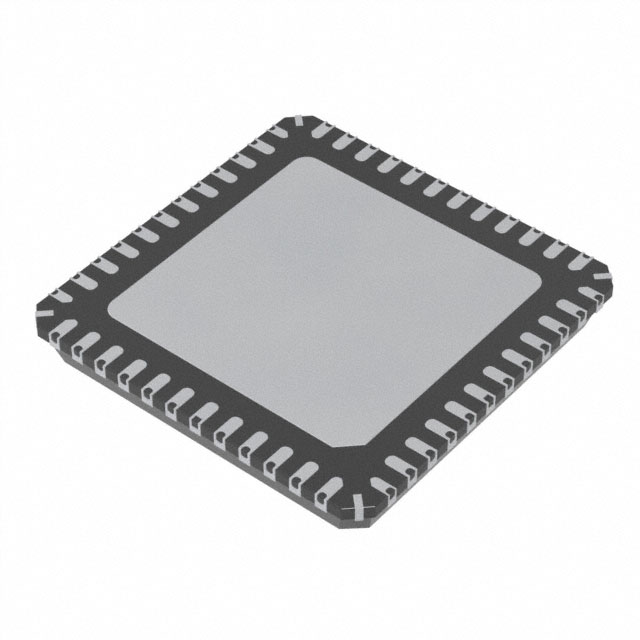


 工商网监
湘ICP备2023018690号
工商网监
湘ICP备2023018690号
