FSUSB20 Low-Power 1-Port High-Speed USB (480Mbps) Switch
September 2006
FSUSB20
Low-Power 1-Port High-Speed USB (480Mbps) Switch
Features
■ −30dB off isolation at 250MHz ■ −30dB non-adjacent channel crosstalk at 250MHz ■ 4.5Ω typical on resistance (RON) ■ −3dB bandwidth: >720MHz ■ Low power consumption (1µA max) ■ Control input: LVTTL compatible ■ Bi-directional operation ■ USB high-speed and full-speed signaling capability ■ Space-saving Pb-free packaging
General Description
FSUSB20 is a low-power high-bandwidth switch specially designed for switching high-speed USB 2.0 signals in handset and consumer applications, such as cell phones, digital cameras, and notebooks with hubs or controllers with limited USB I/Os. The wide bandwidth (>720MHz) of this switch allows signals to pass with minimum edge and phase distortion. Superior channel-tochannel crosstalk results in minimal interference. It is compatible with the high-speed USB 2.0 standard.
Applications
■ Cell phone, PDA, digital camera, and notebook
Ordering Information
Order Number Package Number PbFree
Yes Yes Yes
Top Mark
EY USB20
Package Description
10-Lead MicroPak™, 1.6 x 2.1mm 14-Terminal Depopulated Quad Very-Thin Flat Pack No Leads (DQFN), JEDEC MO-241, 2.5 x 3.0mm
FSUSB20L10X MAC010A FSUSB20BQX MLP014A FSUSB20MUX MUA10A
FSUSB20 10-Lead Molded Small Outline Package (MSOP), JEDEC MO187, 3.0mm Wide
Pb-Free package per JEDEC J-STD-020B.
MicroPak™ is a trademark of Fairchild Semiconductor Corporation.
©2005 Fairchild Semiconductor Corporation FSUSB20 Rev. 1.0.2 www.fairchildsemi.com
�FSUSB20 Low-Power 1-Port High-Speed USB (480Mbps) Switch
Connection Diagrams
Pad Assignments for MicroPak
2B1 2B2 OE
Analog Symbol
1B1 1B2 1A
9
8
7
2A
6 5
2B1 GND 2B2 S Control
2A
VCC 10
1 2 3
4
1B1
1B2
S
1A
OE
(Top View)
Truth Table
Pad Assignments for DQFN
NC
1
S
X Low High
OE
High Low Low
Function
Disconnect A = B1 A = B2
VCC
14 13 OE 12 2B1 11 NC 10 2B2 9
S2 1B1 3 NC 4 1B2 5 1A 6
7 8
Pin Descriptions
Pin Name
OE S A B1–B2
2A
Description
Bus Switch Enable Select Input Bus A Bus B
GND NC
(Top Through View)
Pin Assignment for MSOP
S 1B1 1B2 1A GND
1 2 3 4 5 10 9 8 7 6
VCC OE 2B1 2B2 2A
(Top Through View)
©2005 Fairchild Semiconductor Corporation FSUSB20 Rev. 1.0.2
www.fairchildsemi.com 2
�FSUSB20 Low-Power 1-Port High-Speed USB (480Mbps) Switch
Absolute Maximum Ratings
The “Absolute Maximum Ratings” are those values beyond which the safety of the device cannot be guaranteed. The device should not be operated at these limits. The parametric values defined in the Electrical Characteristics tables are not guaranteed at the absolute maximum ratings. The “Recommended Operating Conditions” table will define the conditions for actual device operation.
Symbol
VCC VS VIN lIK IOUT ICC / IGND TSTG ESD Supply Voltage DC Switch Voltage DC Input Voltage
(1)
Parameter
Min.
−0.5 −0.5V −0.5 −50 50 ±100 −65 All Pins I/O to GND
Max.
+4.6 VCC+0.05 +4.6
Unit
V V mA mA mA
DC Input Diode Current VIN < 0V DC Output Sink Current DC VCC /GND Current Storage Temperature Range Human Body Model
+150 7000 7000
°C V
Notes: 1. The input and output negative voltage ratings may be exceeded if the input and output diode current ratings are observed.
Recommended Operating Conditions(2)
Symbol
VCC VIN VOUT tr,tf TA Power Supply Operating Input Voltage Output Voltage Input Rise and Fall Time Free Air Operating Temperature Switch Control Input Switch I/O
Parameter
Min.
3.0 0 0 0 0 −40
Max.
3.6 VCC VCC 5 DC +85°
Unit
V V V ns/V °C
Notes: 2. Unused control inputs must be held HIGH or LOW. They may not float.
©2005 Fairchild Semiconductor Corporation FSUSB20 Rev. 1.0.2
www.fairchildsemi.com 3
�FSUSB20 Low-Power 1-Port High-Speed USB (480Mbps) Switch
DC Electrical Characteristics
Typical values are at VCC = 3.0V and TA = +25°C.
TA = −40 °C to +85 °C Symbol
VIK VIH VIL II IOFF RON ΔRON
Parameter
Clamp Diode Voltage HIGH Level Input Voltage LOW Level Input Voltage Input Leakage Current Switch On Resistance(3) Delta RON
Conditions
IIN = −18mA
VCC (V)
3.0 3.0 to 3.6 3.0 to 3.6
Min.
2.0
Typ.
Max.
−1.2
Units
V V
0.8 ±1.0 ±1.0 5.0 4.5 0.3 1.0 1.0 7.0 6.5
V μA μA Ω Ω Ω Ω μA
0 ≤ VIN ≤ 3.6V VIN = 0.8V, ION = 8mA VIN = 3.0V, ION = 8mA VIN = 0.8V, VIN = 0V–1.5V, ION = 8mA IOUT = 8mA VIN = VCC or GND, IOUT = 0
3.6 3.6 3.0 3.0 3.0 3.0 3.6
OFF-STATE Leakage Current 0 ≤ A, B ≤ VCC
RFLAT(ON) On Resistance Flatness(4) ICC Quiescent Supply Current
Notes: 3. Measured by the voltage drop between A and B pins at the indicated current through the switch. On resistance is determined by the lower of the voltages on the two (A or B) pins. 4. Flatness is defined as the difference between the maximum and minimum value on resistance over the specified range of conditions.
AC Electrical Characteristics
Typical values are at VCC = 3.3V and TA = +25°C.
TA = −40°C to +85°C Symbol
tON tOFF tPD OIRR XTALK BW
Parameter
Turn ON Time S-to-Bus B Turn OFF Time S-to-Bus B Propagation Delay Non-Adjacent OFF-Isolation Non-Adjacent Channel Crosstalk −3dB Bandwidth
Conditions
VB = 0.8V VB = 0.8V CL = 10pF f = 250MHz, RL = 50Ω f = 250MHz, RL = 50Ω, RL = 50Ω, CL = 0pF RL = 50Ω, CL = 5pF
VCC (V)
3.0 to 3.6 3.0 to 3.6 3.0 to 3.6 3.0 to 3.6 3.0 to 3.6 3.0 to 3.6
Min.
Typ.
4.8 2.2 0.25 −26.0 −45.0 750 435
Figure Max. Units Number
7.0 4.0 ns ns ns dB dB MHz Figure 5 Figure 6 Figure 5 Figure 6 Figure 10 Figure 7 Figure 8 Figure 9
©2005 Fairchild Semiconductor Corporation FSUSB20 Rev. 1.0.2
www.fairchildsemi.com 4
�FSUSB20 Low-Power 1-Port High-Speed USB (480Mbps) Switch
USB Related AC Electrical Characteristics
Typical values are at VCC = 3.3V and TA = +25°C.
TA = −40°C to +85°C Symbol
tSK(O) tSK(P)
Parameter
Channel-to-Channel Skew Skew of Opposite Transition of the Same Output Total Jitter
Conditions
CL = 10pF CL = 10pF
VCC (V)
3.0 to 3.6 3.0 to 3.6
Min.
Typ.
0.051 0.020
Max.
Units
ns ns
Figure Number
Figure 10 Figure 11 Figure 10 Figure 11
TJ
RL = 50Ω, CL = 10pF tR = tF = 750ps at 480Mbps
3.0 to 3.6
0.170
ns
Capacitance
Typical values are at VCC = 3.3V and TA = +25°C.
TA = −40°C to +85°C Symbol
CIN CON COFF
Parameter
Control Pin Input Capacitance A/B ON Capacitance Port B OFF Capacitance
Conditions
VCC = 0V VCC = 3.3V, OE = 0V VCC and OE = 3.3V
Typ.
2.5 12.0 4.0
Units
pF pF pF
©2005 Fairchild Semiconductor Corporation FSUSB20 Rev. 1.0.2
www.fairchildsemi.com 5
�FSUSB20 Low-Power 1-Port High-Speed USB (480Mbps) Switch
Typical Characteristics
Frequency Response
0 -1 -2 -3 Gain (dB) -4 -5 -6 -7 -8 1 10 100 Frequency (MHz) 1000 10000
CL = 0pF, VCC = 3.3V
Figure 1. Gain vs. Frequency
Frequency Response
0 -10 -20 -30 -40 -50 -60 -70 -80 -90 -100 -110 -120 1 10 Frequency (MHz) 100 1000
Off Isolation (dB)
VBIAS = 0.5V, VCC = 3.3V
Figure 2. OFF Isolation
©2005 Fairchild Semiconductor Corporation FSUSB20 Rev. 1.0.2
www.fairchildsemi.com 6
�FSUSB20 Low-Power 1-Port High-Speed USB (480Mbps) Switch
Typical Characteristics (Continued)
Frequency Response
0 -10 -20 -30 -40 -50 -60 -70 -80 -90 -100 -110 -120 1
Crosstalk (dB)
10 Frequency (MHz)
100
1000
VBIAS = 0.5V, VCC = 3.3V
Figure 3. Crosstalk
10.0 9.0 8.0 RON (Ohms) 7.0 6.0 5.0 4.0 3.0 2.0 1.0 0.0 0.00 0.50 1.00 -25°C VB2 = 800.000mV RON = 4.437Ω 1.50 2.00 2.50 3.00 -40°C VB2 = 800.000mV RON = 3.561Ω -85°C VB2 = 800.000mV RON = 5.402Ω
VB2 (V)
Figure 4. RON
©2005 Fairchild Semiconductor Corporation FSUSB20 Rev. 1.0.2
www.fairchildsemi.com 7
�FSUSB20 Low-Power 1-Port High-Speed USB (480Mbps) Switch
AC Loading and Waveforms
nB1 nB2
+ VB –
A 50Ω Control GND 10 pF
Note: Input driven by 50Ω source terminated in 50Ω Note: CL includes load and stray capacitance Note: Input PRR = 1.0 MHz, tW = 500ns Figure 5. AC Test Circuit
GND S OE
tr = 2.5ns SELECT INPUT 10% tON 90% OUTPUT 90% 1.5V 90% 1.5V
tf = 2.5ns 3.0V
10% tOFF 90%
GND VOH
VOL
Figure 6. AC Waveforms
B1 50Ω B2
A Network Analyzer 50Ω
B1 100Ω
A 100Ω
Network Analyzer
S Control
S Control
50Ω
OE
OE
Figure 7. OFF Isolation Test
Figure 8. Crosstalk Test
B
A Network Analyzer 50Ω
S Control GND
OE
Figure 9. Bandwidth Test
©2005 Fairchild Semiconductor Corporation FSUSB20 Rev. 1.0.2
www.fairchildsemi.com 8
�FSUSB20 Low-Power 1-Port High-Speed USB (480Mbps) Switch
AC Loading and Waveforms (Continued)
800 mV Input 400 mV tPLH Output tPHL VOH VOL
Figure 10. Propagation Delay
800 mV
50% Input
50% 400 mV 0 tPHL VOH
tPLH
50% Output tSK(P) = | tPHL - tPHL |
50%
VOL
Figure 11. Pulse Skew tSK(P)
800 mV
50% Input tPLH1 tPHL1 0
50% 400 mV
50% Output 1 tSK(O) tSK(O)
50%
50% Output 2 tPLH2 tSK(O) = | tPLH1 - tPLH2 | or | tPHL1 - tPHL2 | tPHL2
50%
Figure 12. Output Skew tSK(O)
©2005 Fairchild Semiconductor Corporation FSUSB20 Rev. 1.0.2
www.fairchildsemi.com 9
�FSUSB20 Low-Power 1-Port High-Speed USB (480Mbps) Switch
Tape and Reel Specifications
Tape Format for MicroPak
Dimensions are in millimeters unless otherwise noted.
Package Designator
L10X
Tape Section
Leader (Start End) Carrier Trailer (Hub End)
Number Cavities
125 (typ) 5000 75 (typ)
Cavity Status
Empty Filled Empty
Cover Tape Status
Sealed Sealed Sealed
Tape Dimension
Dimensions are in millimeters unless otherwise noted.
©2005 Fairchild Semiconductor Corporation FSUSB20 Rev. 1.0.2
www.fairchildsemi.com 10
�FSUSB20 Low-Power 1-Port High-Speed USB (480Mbps) Switch
Reel Dimension for MicroPak
Dimensions are in inches (millimeters) unless otherwise noted.
Tape Size
(8mm)
A
7.0 (177.8)
B
0.059 (1.50)
C
0.512 (13.00)
D
0.795 (20.20)
N
2.165 (55.00)
W1
0.331 +0.059/−0.000 (8.40 +1.50/−0.00)
W2
0.567 (14.40)
W3
W1 +0.078/−0.039 (W1 +2.00/−1.00)
©2005 Fairchild Semiconductor Corporation FSUSB20 Rev. 1.0.2
www.fairchildsemi.com 11
�FSUSB20 Low-Power 1-Port High-Speed USB (480Mbps) Switch
Tape Format for DQFN
Dimensions are in millimeters unless otherwise notes.
Package Designator
BQX
Tape Section
Leader (Start End) Carrier Trailer (Hub End)
Number Cavities
125 (typ) 2500/3000 75 (typ)
Cavity Status
Empty Filled Empty
Cover Tape Status
Sealed Sealed Sealed
Tape Dimensions
Dimensions are in millimeters unless otherwise noted.
©2005 Fairchild Semiconductor Corporation FSUSB20 Rev. 1.0.2
www.fairchildsemi.com 12
�FSUSB20 Low-Power 1-Port High-Speed USB (480Mbps) Switch
Tape Dimensions for MSOP
Dimensions are in inches (millimeters) unless otherwise specified.
Reel Dimensions for MSOP
Dimensions are in inches (millimeters) unless otherwise specified
Tape Size
(12mm)
A
13 (330)
B
0.059 (1.5)
C
0.512 (13)
D
0.795 (20.2)
N
7.008 (178)
W1
0.448 (12.4)
W2
0.724 (18.4)
W3
0.468-0.606 (11.9 -15.4)
©2005 Fairchild Semiconductor Corporation FSUSB20 Rev. 1.0.2
www.fairchildsemi.com 13
�FSUSB20 Low-Power 1-Port High-Speed USB (480Mbps) Switch
Physical Dimensions (Continued)
Dimensions are in millimeters unless otherwise noted.
Figure 13. 10-Lead MicroPak, 1.6 x 2.1mm
©2005 Fairchild Semiconductor Corporation FSUSB20 Rev. 1.0.2
www.fairchildsemi.com 14
�FSUSB20 Low-Power 1-Port High-Speed USB (480Mbps) Switch
Physical Dimensions (Continued)
Dimensions are in millimeters unless otherwise noted.
Figure 14. 14-Terminal Depopulated Quad Very-Thin Flat Pack No Leads (DQFN), JEDEC MO-241, 2.5 x 3.0mm
©2005 Fairchild Semiconductor Corporation FSUSB20 Rev. 1.0.2
www.fairchildsemi.com 15
�FSUSB20 Low-Power 1-Port High-Speed USB (480Mbps) Switch
Physical Dimensions (Continued)
Dimensions are in millimeters unless otherwise noted.
Figure 15. 10-Lead Molded Small Outline Package (MSOP), JEDEC MO-187, 3.0mm Wide
©2005 Fairchild Semiconductor Corporation FSUSB20 Rev. 1.0.2
www.fairchildsemi.com 16
�FSUSB20 Low-Power 1-Port High-Speed USB (480Mbps) Switch
©2005 Fairchild Semiconductor Corporation FSUSB20 Rev. 1.0.2
www.fairchildsemi.com 17
�
很抱歉,暂时无法提供与“FSUSB20L10X”相匹配的价格&库存,您可以联系我们找货
免费人工找货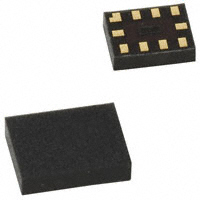


 工商网监
湘ICP备2023018690号
工商网监
湘ICP备2023018690号
