SC553
NOT RECOMMENDED FOR NEW DESIGN
150mA Ultra Low Dropout
Regulator with Adjustable Output
POWER MANAGEMENT
Description
Features
The SC553 is a low dropout linear regulator that
operates from a +2.25V to +6.5V input range and
delivers up to 150mA. A PMOS pass transistor allows
the low 75µA supply current to remain independent of
load, making these devices ideal for battery operated
portable equipment such as cellular phones, cordless
phones and personal digital assistants.
! “5205” compatible pinout
! 2% output accuracy guaranteed over line, load and
!
!
!
!
!
!
!
!
!
N
O
FO T R
R EC
N O
EW M
M
D EN
ES D
IG ED
N
The SC553 has an adjust pin (ADJ) enabling the user to
set the output voltage anywhere from 1.25V to 6V. For a
low noise version, see SC1453 and for an error flag see
SC1457. Other features include low powered shutdown,
short circuit protection, thermal shutdown protection and
reverse battery protection. The SC553 comes in the tiny
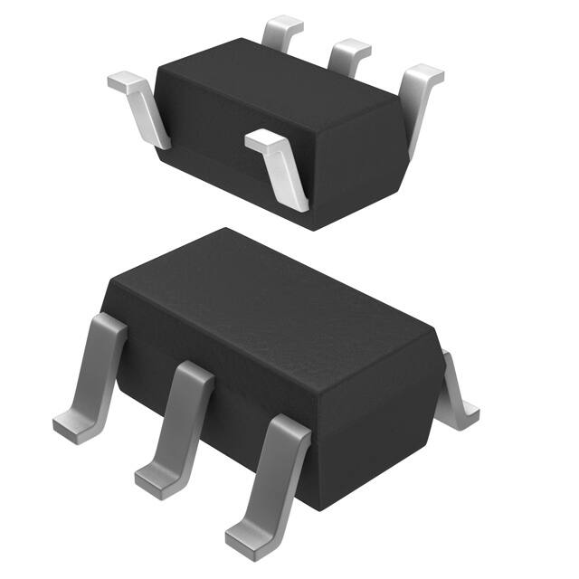
5 lead SOT-23 package.
temperature
Guaranteed 150 mA output current
Very small external components - designed to work
with ceramic capacitors
Output adjustable from 1.25V to 6V
Very low supply current
Thermal overload protection
Reverse battery protection
Low power shutdown
Full industrial temperature range
Surface mount packaging (5 pin SOT-23)
Applications
!
!
!
!
!
!
!
Battery Powered Systems
Cellular Telephones
Cordless Telephones
Personal Digital Assistants
Portable Instrumentation
Modems
PCMCIA cards
Typical Application Circuit
VIN
1
C1
1uF
3
U1
SC553
IN
OUT
EN
GND ADJ
5
4
R1
VOUT
C2
1uF
R1
VOUT = 1.250 • 1 +
R2
2
R2
Revision: April 20, 2004
Downloaded from Elcodis.com electronic components distributor
1
www.semtech.com
�SC553
NOT RECOMMENDED FOR NEW DESIGN
POWER MANAGEMENT
Absolute Maximum Ratings
Exceeding the specifications below may result in permanent damage to the device, or device malfunction. Operation outside of the parameters specified
in the Electrical Characteristics section is not implied.
Symbol
Maximum
Units
Input Supply Voltage
VIN
-0.6 to +7
V
Enable Voltage
V EN
-0.6 to VIN
V
Output Pin Voltage
VOUT
-0.6 to +7
V
Adjust Pin Voltage
V AD J
-0.6 to +7
V
Thermal Resistance Junction to Ambient
θJA
256
°C/W
Thermal Resistance Junction to Case
θJC
81
°C/W
N
O
FO T R
R EC
N O
EW M
M
D EN
ES D
IG ED
N
Parameter
Operating Ambient Temperature Range
TA
-40 to +85
°C
Operating Junction Temperature Range
TJ
-40 to +125
°C
Storage Temperature Range
TSTG
-65 to 150
°C
Lead Temperature (Soldering) 10 Sec.
TLEAD
300
°C
Electrical Characteristics
Unless specified: VIN = 2.25V, VEN = VIN, IOUT = 100µA, CIN = COUT = 1µF, TA = 25°C. Values in bold apply over full operating ambient temperature range.
Parameter
IN
Symbol
Supply Voltage Range
VIN
Supply Current
IQ
Off-State Supply Current
IQ(OFF)
Conditions
Min
Typ
2.25
IOUT = 0mA to150mA, 2.25V ≤ VIN ≤ 6.5V
VIN = 6.5V, VEN = 0V
75
Max
Units
6.50
V
130
µA
160
0.1
1.0
µA
1.5
ADJ
Adjust Pin Voltage (1)
Adjust Pin Input Current (2)
V AD J
IADJ
IOUT = 1mA
-1.5%
0mA ≤ IOUT ≤ 150mA, 2.25V ≤ VIN ≤ 5.5V
-2.0%
VADJ = 1.3V
1.250
+1.5%
V
+2.0%
0.015
2.500
nA
5.000
OUT
Line Regulation (1)
REG(LINE)
VIN = 2.25V to 5.5V, IOUT = 1mA, VADJ = VOUT
1.5
10
mV
12
Load Regulation (1)
REG(LOAD)
IOUT = 0.1mA to 150mA,
VIN = 2.25V, VADJ = VOUT
2004 Semtech Corp.
Downloaded from Elcodis.com electronic components distributor
2
-1
-10
mV
-20
www.semtech.com
�SC553
NOT RECOMMENDED FOR NEW DESIGN
POWER MANAGEMENT
Electrical Characteristics (Cont.)
Unless specified: VIN = 2.25V, VEN = VIN, IOUT = 100µA, CIN = COUT = 1µF, TA = 25°C. Values in bold apply over full operating ambient temperature range.
Parameter
Symbol
Conditions
Min
Typ
Max
Units
OUT (Cont.)
Current Limit
ILIM
Dropout Voltage(1)(3)
VD
400
mA
IOUT = 1mA
1
IOUT = 50mA
50
mV
65
mV
75
N
O
FO T R
R EC
N O
EW M
M
D EN
ES D
IG ED
N
IOUT = 100mA
100
Enable Input Threshold
Enable Input Bias Current (2)
VIH
2.25V ≤ VIN ≤ 6.5V
VIL
2.25V ≤ VIN ≤ 6.5V
IEN
0V ≤ VEN ≤ VIN
mV
155
IOUT = 150mA
EN
125
150
190
mV
230
1.6
V
0.4
-0.5
0
+0.5
µA
Over Temperature Protection
High Trip Level
Hysteresis
THI
150
°C
THYST
15
°C
Notes:
(1) Low duty cycle pulse testing with Kelvin connections required.
(2) Guaranteed by design.
(3) VOUT = 3.3V. Defined as the input to output differential at which the output voltage drops 100mV below the value
measured at a differential of 1V. Not measurable on outputs set below 2.25V due to minimum VIN constraints. See
Typical Characteristics for typical dropout voltage at other output voltage settings.
2004 Semtech Corp.
Downloaded from Elcodis.com electronic components distributor
3
www.semtech.com
�NOT RECOMMENDED FOR NEW DESIGN
POWER MANAGEMENT
Pin Configuration
SC553
Ordering Information
Top View
Part Number (1)
P ackag e
SC553ISKTR
SOT-23-5
SC553ISKTRT(2)
Notes:
(1) Only available in tape and reel packaging. A reel
contains 3000 devices.
(2) Lead free product. This product is fully WEEE and
RoHS compliant.
SOT-23-5L
N
O
FO T R
R EC
N O
EW M
M
D EN
ES D
IG ED
N
Pin Descriptions
Pin #
Pin Name
1
IN
2
GND
3
EN
4
AD J
5
OUT
Block Diagram
Pin Function
Input pin.
Ground pin. Can be used for heatsinking if needed.
Active high enable pin. Connect to IN if not being used.
Adjust pin. Connecting this pin to an external resistor divider (see Typical Application Circuit
on page 1) sets VOUT to:
R1
VOUT = 1.250 • 1 +
R
2
Regulator output, sourcing up to 150mA.
2004 Semtech Corp.
Downloaded from Elcodis.com electronic components distributor
4
www.semtech.com
�SC553
NOT RECOMMENDED FOR NEW DESIGN
POWER MANAGEMENT
Marking Information
Top Mark
Bottom Mark
553
yyww
yyww = Datecode (Example: 0108)
Theory Of Operation
N
O
FO T R
R EC
N O
EW M
M
D EN
ES D
IG ED
N
Applications Information
Component Selection - General
The SC553 is intended for applications where very low
dropout voltage, low supply current and low output noise
are critical. It provides a very simple, low cost solution
that uses very little pcb real estate. Only two external
capacitors are required for operation.
Output capacitor - Semtech recommends a minimum
capacitance of 1µF at the output with an equivalent
series resistance (ESR) of < 1Ω over temperature. While
the SC553 has been designed to be used with ceramic
capacitors, it does not have to be used with ceramic
capacitors, allowing the designer a choice. Increasing the
bulk capacitance will further reduce output noise and
improve the overall transient response.
The SC553 contains a bandgap reference trimmed for
optimal temperature coefficient which is fed into the
inverting input of an error amplifier. The output voltage
of the regulator is divided down externally using a
resistor divider and compared to the bandgap voltage
via the adjust pin (ADJ). The error amplifier drives the
gate of a low RDS(ON) P-channel MOSFET pass device to
maintain VOUT such that VADJ = VREF.
An active high enable pin (EN) allows the regulator to be
shut down. Pulling this pin low causes the device to
enter a very low power shutdown mode, where it will draw
typically 0.1µA from the input supply.
Input capacitor - Semtech recommends the use of a
1µF ceramic capacitor at the input. This allows for the
device being some distance from any bulk capacitance
on the rail. Additionally, input droop due to load transients
is reduced, improving overall load transient response.
External voltage selection resistors - the use of 1%
resistors, and designing for a current flow ≥ 10µA is
recommended to ensure a well regulated output (thus
R2 ≤ 125kΩ). The output voltage (referring to Figure 1
below) will be:
The regulator has its own current limit circuitry to
ensure that the output current will not damage the
device during output short, overload or start-up. The
current limit is guaranteed to be greater than 400mA to
allow fast charging of the output capacitor and high
initial currents for DSP initialization.
R1
VOUT = 1.250 • 1 +
R
2
1
VIN
The SC553 includes thermal shutdown circuitry to turn
off the device if T J exceeds 150°C (typical), with the
device remaining off until TJ drops by 15°C (typical).
Reverse battery protection circuitry ensures that the
device cannot be damaged if the input supply is
accidentally reversed, limiting the reverse current to less
than 1.5mA.
2004 Semtech Corp.
Downloaded from Elcodis.com electronic components distributor
C1
1uF
3
U1
SC553
IN
OUT
EN
GND ADJ
5
4
VOUT
R1
C2
1uF
2
R2
Figure 1
5
www.semtech.com
�SC553
NOT RECOMMENDED FOR NEW DESIGN
POWER MANAGEMENT
Applications Information (Cont.)
Thermal Considerations
Layout Considerations
The worst-case power dissipation for this part is given
by:
While layout for linear devices is generally not as critical
as for a switching application, careful attention to detail
will ensure reliable operation.
PD(MAX ) = (VIN(MAX) − VOUT(MIN) ) • IOUT(MAX ) + VIN(MAX ) • IQ(MAX )
(1)
1) Attaching the part to a larger copper footprint will
enable better heat transfer from the device, especially
on PCBs where there are internal ground and power
planes.
For all practical purposes, equation (1) can be reduced
to the following expression:
(2)
N
O
FO T R
R EC
N O
EW M
M
D EN
ES D
IG ED
N
2) Place the input and output capacitors close to the
device for optimal transient response and device
behaviour.
Looking at a typical application, 3.3V to 2.8V at 150mA:
VIN(MAX) = 3.3 + 5% = 3.465V
VOUT(MIN) = 2.8V - 2% = 2.744V
IOUT = 150mA
TA = 85°C
3) While the external resistor divider does not need to be
close to the device, care should be taken to avoid routing
the connections next to any lines carrying large amounts
of noise. The simplest solution is to place these resistors
close to the device and routing the top of R1 to the load
if not adjacent to the part.
Inserting these values into equation (2) gives us:
4) Connect all ground connections directly to the ground
plane. If there is no ground plane, connect to a common
local ground point before connecting to board ground.
Using this figure, we can calculate the maximum thermal
impedance allowable to maintain TJ ≤ 125°C:
θ JA (MAX ) =
(T
J(MAX )
− TA (MAX ) )
PD(MAX )
=
Typical Characteristics
(125 − 85) = 370°C / W
Dropout Voltage vs. Output Voltage
0.108
vs. Output Current
250
With the standard SOT-23-5 Land Pattern shown at the
end of this datasheet, and minimum trace widths, the
thermal impedance junction to ambient for SC553 is
256°C/W. Thus no additional heatsinking is required for
this example.
225
200
Downloaded from Elcodis.com electronic components distributor
Top to bottom:
IOUT = 150mA
IOUT = 100mA
IOUT = 50mA
VD (mV)
175
The junction temperature can be reduced further (or
higher power dissipation can be allowed) by the use of
larger trace widths and connecting PCB copper to the
GND pin (pin 2), which connects directly to the device
substrate. Adding approximately one square inch of PCB
copper to pin 2 will reduce θ JA to approximately
130°C/W and T J(MAX) for the example above to
approximately 100°C. The use of multi layer boards with
internal ground/power planes will lower the junction
temperature and improve overall output voltage
accuracy.
2004 Semtech Corp.
TA = 25°C
150
125
100
75
50
25
0
2.0
2.5
3.0
3.5
4.0
4.5
5.0
5.5
6.0
VOUT (V)
6
www.semtech.com
�NOT RECOMMENDED FOR NEW DESIGN
SC553
N
O
FO T R
R EC
N O
EW M
M
D EN
ES D
IG ED
N
POWER MANAGEMENT
Outline Drawing - SOT-23-5
Land Pattern - SOT-23-5
This land pattern is for reference only. Consult your
manufacturing group to ensure you meet your
company’s manufacturability guidelines.
Contact Information
Semtech Corporation
Power Management Products Division
200 Flynn Road, Camarillo, CA 93012
Phone: (805)498-2111 FAX (805)498-3804
2004 Semtech Corp.
Downloaded from Elcodis.com electronic components distributor
7
www.semtech.com
�


 工商网监
湘ICP备2023018690号
工商网监
湘ICP备2023018690号
