CMOS Quad 2-Input NAND Schmitt Triggers
CD4093B
FEATURES
• Wide Operating Voltage Range of 3.0V to 18.0V
• Maximum Input Current of 1µA at 18V over Full
Package-Temperature range, 100nA at 18V and 25°C
• Independent Schmitt-Trigger at each Input
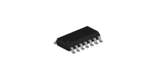
SOP-14
APPLICATIONS
•
•
•
•
•
Wave and Pulse Shapers
High-Noise-Environment Systems
Monostable Multivibrators
Asstable Multivibtayors
NAND Logic
DIP-14
DESCRIPTION
ORDERING INFORMATION
The CD4093B consist of four Schmitt-trigger circuits.
Each circuit functions as a two-input NAND gate with
Schmitt-trigger action on both inputs.
The gate
switches at different points for positive- and negativegoing signals. The difference between the positive
voltage (VTP) and the negative voltage (VTN) is defined
as hysteresis voltage (VH).
Device
Package
CD4093BD
SOP-14
CD4093BN
DIP-14
ABSOLUTE MAXIMUM RATINGS (Note 1)
CHARACTERISTIC
SYMBOL
MIN.
MAX.
UNIT
DC Supply Voltage (Referenced to VSS)
VDD
-0.5
20
V
DC Input Voltage (Referenced to VSS)
VIN
-0.5
VDD + 0.5
V
DC Input Current
IIN
-
±10
mA
Maximum Junction Temperature
TJ
-
150
°C
TSTG
-65
150
°C
Storage Temperature
Note1. Stresses beyond those listed under Absolute Maximum Ratings may cause permanent damage to the device. These
are stress ratings only and functional operation of the device at these or any other conditions beyond those indicated
under Recommended Operating Conditions is not implied. Exposure to absolute-maximum-rated conditions for
extended periods may affect device reliability.
Feb. 2020 – R1.1.2
1/9
HTC
�CMOS Quad 2-Input NAND Schmitt Triggers
CD4093B
RECOMMENDED OPERATING CONDITIONS (Note 2)
CHARACTERISTIC
SYMBOL
MIN.
MAX.
UNIT
Supply Voltage
VDD
3
18
V
DC Input Voltage
VIN
0
VDD
V
VOUT
0
VDD
V
TA
-55
125
°C
DC Output Voltage
Operating Free-Air Temperature Range
Note 2. The device is not guaranteed to function outside its operating ratings.
ORDERING INFORMATION
Package
Order No.
Description
Supplied As
Status
SOP-14
CD4093BD
Quad 2-Input NAND Schmitt Triggers
Tape & Reel
Active
DIP-14
CD4093BN
Quad 2-Input NAND Schmitt Triggers
Tube
Active
Feb. 2020 – R1.1.2
2/9
HTC
�CMOS Quad 2-Input NAND Schmitt Triggers
CD4093B
PIN CONFIGURATION
SOP-14
DIP-14
1A
1
14
VDD
1A
1
14
VDD
1B
2
13
4B
1B
2
13
4B
1Y
3
12
4A
1Y
3
12
4A
2Y
4
11
4Y
2Y
4
11
4Y
2A
5
10
3Y
2A
5
10
3Y
2B
6
9
3B
2B
6
9
3B
VSS
7
8
3A
VSS
7
8
3A
PIN DESCRIPTION
Pin No.
Pin Name
Pin Function
SOP-14
DIP-14
1
1
1A
Input 1A
2
2
1B
Input 1B
3
3
1Y
Output 1
4
4
2Y
Output 2
5
5
2A
Input 2A
6
6
2B
Input 2B
7
7
VSS
Ground
8
8
3A
Input 3A
9
9
3B
Input 3B
10
10
3Y
Output 3
11
11
4Y
Output 4
12
12
4A
Input 4A
13
13
4B
Input 4B
14
14
VDD
Feb. 2020 – R1.1.2
Power Supply
3/9
HTC
�CMOS Quad 2-Input NAND Schmitt Triggers
CD4093B
BLOCK DIAGRAM
1A
1Y
1B
2A
2Y
2B
3A
3Y
3B
4A
4Y
4B
Feb. 2020 – R1.1.2
4/9
HTC
�CMOS Quad 2-Input NAND Schmitt Triggers
CD4093B
DC ELECTRICAL CHARACTERISTICS
Voltages referenced to VSS.
Limit
SYMBOL
VTP.min
PARAMETER
Minimum Positive-Going
Input Threshold Voltage
TEST CONDITION
Input on Terminal A or B;
Other Inputs to VDD
Input on Terminal A and B;
Other Inputs to VDD
VTP.max
Maximum Positive-Going
Input Threshold Voltage
Input on Terminal A or B;
Other Inputs to VDD
Input on Terminal A and B;
Other Inputs to VDD
VTN.min
Minimum Negative-Going
Input Threshold Voltage
Input on Terminal A or B;
Other Inputs to VDD
Input on Terminal A and B;
Other Inputs to VDD
VTN.max
Maximum Negative-Going
Input Threshold Voltage
Input on Terminal A or B;
Other Inputs to VDD
Input on Terminal A and B;
Other Inputs to VDD
VH.min
VH.max
Minimum Hysteresis Voltage
Maximum Hysteresis Voltage
Feb. 2020 – R1.1.2
Input on Terminal A and/or B;
Other Inputs to VDD
Input on Terminals A and/or B;
Other Inputs to VDD
5/9
VDD
UNIT
−55°C
25°C
125°C
5V
2.2
2.2
2.2
10 V
4.6
4.6
4.6
15 V
6.8
6.8
6.8
5V
2.6
2.6
2.6
10 V
5.6
5.6
5.6
15 V
6.3
6.3
6.3
5V
3.6
3.6
3.6
10 V
7.1
7.1
7.1
15 V
10.8
10.8
10.8
5V
4.0
4.0
4.0
10 V
8.2
8.2
8.2
15 V
12.7
12.7
12.7
5V
0.9
0.9
0.9
10 V
2.5
2.5
2.5
15 V
4.0
4.0
4.0
5V
1.4
1.4
1.4
10 V
3.4
3.4
3.4
15 V
4.8
4.8
4.8
5V
2.8
2.8
2.8
10 V
5.2
5.2
5.2
15 V
7.4
7.4
7.4
5V
3.2
3.2
3.2
10 V
6.6
6.6
6.6
15 V
9.6
9.6
9.6
5V
0.3
0.3
0.3
10 V
1.2
1.2
1.2
15 V
1.6
1.6
1.6
5V
1.6
1.6
1.6
10 V
3.4
3.4
3.4
15 V
5.0
5.0
5.0
V
V
V
V
V
V
HTC
�CMOS Quad 2-Input NAND Schmitt Triggers
CD4093B
DC ELECTRICAL CHARACTERISTICS (continued)
Voltages referenced to VSS.
Limit
SYMBOL
VOH
VOL
IIN
ICC
IOL
IOH
PARAMETER
TEST CONDITION
Minimum High-Level Output
Voltage
Maximum Low-Level Output
Voltage
Maximum Input Leakage
Current
Minimum Output Low (Sink)
Current
25°C
125°C
5V
4.95
4.95
4.95
10 V
9.95
9.95
9.95
15 V
14.95
14.95
14.95
5V
0.05
0.05
0.05
10 V
0.05
0.05
0.05
15 V
0.05
0.05
0.05
18 V
±0.1
±0.1
±1.0
5V
1
1
30
10 V
2
2
60
15 V
4
4
120
20 V
20
20
600
VOL = 0.4V
5V
0.64
0.51
0.36
VOL = 0.5V
10 V
1.6
1.3
0.9
VOL = 1.5V
15 V
4.2
3.4
2.4
VOH = 2.5V
5V
−2.0
−1.6
−1.15
VOH = 4.6V
5V
−0.64
−0.51
−0.36
VOH = 9.5V
10 V
−1.6
−1.3
−0.9
VOH = 13.5V
15 V
−4.2
−3.4
−2.4
VIN = VDD or VSS
VIN = VDD
Minimum Output High
(Source) Current
VIN = VDD or VSS
VIN = VDD or VSS
VIN = VDD or VSS
UNIT
−55°C
VIN = VDD or VSS
Maximum Quiescent Supply
Current
VDD
V
V
µA
µA
mA
mA
AC ELECTRICAL CHARACTERISTICS
CL = 50 pF, RL = 200kΩ, Input tr = tf = 20 ns
Limit
SYMBOL
tPLH,
tPHL
tTLH,
tTHL
CIN
PARAMETER
VDD
Maximum Propagation Delay, Input A or Input B to Output Y
(Figure 4)
Maximum Output Transition Time, Any Output
(Figure 4)
Maximum Input Capacitance
Feb. 2020 – R1.1.2
25°C
125°C
5V
380
380
760
10 V
180
180
360
15 V
130
130
260
5V
200
200
400
10 V
100
100
200
15 V
80
80
160
–
6/9
UNIT
−55°C
7.5
ns
ns
pF
HTC
�CMOS Quad 2-Input NAND Schmitt Triggers
CD4093B
FUNCTION TABLE
Input (A)
Input (B)
Output (Y)
L
L
H
L
H
H
H
L
H
H
H
L
SWITCHING CHARACTERISTICS
VTP
VTN
VDD
VIN
VH
VOUT
VH
VH = VTP - VTN
VSS
VDD
VOUT
VIN
VTN
VSS
Fig. 1. Hysteresis Definition
VTP
Fig. 2. Hysteresis Characteristic
tr
tf
VDD
90%
VIN
50%
10%
VSS
VDD
VOUT
tPHL
tPLH
VIN
VOH
90%
VOUT
50%
10%
tTHL
Fig. 3. Test Circuit
Feb. 2020 – R1.1.2
VOL
tTLH
Fig. 4. Switching Time Waveforms
7/9
HTC
�CMOS Quad 2-Input NAND Schmitt Triggers
CD4093B
TYPICAL OPERATING CHARACTERISTICS
T.B.D.
Feb. 2020 – R1.1.2
8/9
HTC
�CMOS Quad 2-Input NAND Schmitt Triggers
CD4093B
REVISION NOTICE
The description in this data sheet is subject to change without any notice to describe its electrical characteristics
properly.
Feb. 2020 – R1.1.2
9/9
HTC
�
很抱歉,暂时无法提供与“CD4093BD”相匹配的价格&库存,您可以联系我们找货
免费人工找货- 国内价格
- 54+2.21120
- 100+1.87950
- 500+1.49250
- 1000+1.29350
- 10000+1.24930
- 国内价格
- 1+1.25550
- 10+1.20900
- 100+1.06950
- 500+1.04160
- 国内价格
- 54+2.21120
- 100+1.87950
- 500+1.49250
- 1000+1.29350
- 10000+1.24930
- 国内价格
- 54+2.21120
- 100+1.87950
- 500+1.49250
- 1000+1.29350
- 10000+1.24930


 工商网监
湘ICP备2023018690号
工商网监
湘ICP备2023018690号
