60V, 3A, 150kHz, Step-down Switching Regulator
FEATURES
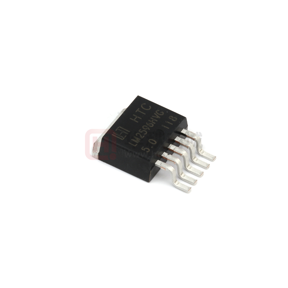
LM2596HV
SOP-8PP PKG
3.3V, 5V, 12V and Adjustable output versions
Adjustable version output voltage range, 1.23V to 57V
±4% max over line and load condition
Available in TO-220, TO-263 and SOP-8PP
Guaranteed 3A output load current
Input voltage range up to 60V
Requires only 4 external components
Excellent line and load regulation specifications
150kHz fixed frequency internal oscillator
Low power standby mode, ISTB typically 30uA
High efficiency
Thermal shutdown and current limit protection
Output short protection by reduction of frequency
by 3 times
TO-263 PKG
TO-220 PKG
ORDERING INFORMATION
Device
LM2596HVGDP-ADJ
LM2596HVGDP-X.X
LM2596HVGR-ADJ
LM2596HVGR-X.X
LM2596HVGT-ADJ
LM2596HVGT-X.X
X.X = Output Voltage = 3.3, 5.0, 12
APPLICATION
Simple high-efficiency step-down (buck) regulator
Efficient pre-regulator for linear regulators
On-card switching regulators
Package
SOP-8PP
TO-263 5L
TO-220 5L
DESCRIPTION
The LM2596HV series of regulators are monolithic integrated circuits that provide all the active functions for a
step-down (buck) switching regulator, capable of driving a 3A load with excellent line and load regulation. These
devices are available in fixed output voltages of 3.3V, 5V, 12V, and an adjustable output version.
Available in a standard 5-lead TO-220 package and a 5-lead TO-263 surface mount package.
External shutdown is included, featuring typically 30 μA standby current. The output switch includes cycle-bycycle current limiting, as well as thermal shutdown, and protection from output short for full protection under fault
conditions.
Absolute Maximum Ratings (Note 1)
CHARACTERISTIC
Supply Voltage
ON/OFF Pin Input Voltage
SYMBOL
MIN.
MAX.
UNIT
VIN
-
63
V
VON/OFF
-0.3
60 (or VIN)
V
FB pin voltage
VFB
-0.3
25 (or VIN)
V
Output voltage to GND
VOUT
-1
Storage Temperature Range
TSTG
-65
150
℃
Maximum Junction Temperature Range
TJ,MAX
-
150
℃
Feb. 2020 – R1.1
-1-
V
HTC
�60V, 3A, 150kHz, Step-down Switching Regulator
LM2596HV
Operating Ratings
CHARACTERISTIC
Supply Voltage
Load Current
Temperature Range
SYMBOL
MIN.
MAX.
UNIT
VIN
4.5
60
V
ILOAD
-
3.0
A
TJ
-40
125
℃
Ordering Information
VOUT
ADJ
3.3V
5.0V
12V
Package
Order No.
Description
Supplied As
Status
SOP-8PP-8L
LM2596HVGDP-ADJ
3A, 150kHz, Adjustable
Reel
Active
TO-263-5L
LM2596HVGR-ADJ
3A, 150kHz, Adjustable
Reel
Active
TO-220-5L
LM2596HVGT-ADJ
3A, 150kHz, Adjustable
Tube
Active
SOP-8PP-8L
LM2596HVGDP-3.3
3A, 150kHz, Fixed
Reel
Contact us
TO-263-5L
LM2596HVGR-3.3
3A, 150kHz, Fixed
Reel
Active
TO-220-5L
LM2596HVGT-3.3
3A, 150kHz, Fixed
Tube
Contact us
SOP-8PP-8L
LM2596HVGDP-5.0
3A, 150kHz, Fixed
Reel
Active
TO-263-5L
LM2596HVGR-5.0
3A, 150kHz, Fixed
Reel
Active
TO-220-5L
LM2596HVGT-5.0
3A, 150kHz, Fixed
Tube
Active
SOP-8PP-8L
LM2596HVGDP-12
3A, 150kHz, Fixed
Reel
Contact us
TO-263-5L
LM2596HVGR-12
3A, 150kHz, Fixed
Reel
Active
TO-220-5L
LM2596HVGT-12
3A, 150kHz, Fixed
Tube
Active
Feb. 2020 – R1.1
-2-
HTC
�60V, 3A, 150kHz, Step-down Switching Regulator
LM2596HV
PIN CONFIGURATION
VIN 1.
VOUT 2.
FB/ADJ 3.
On/Off 4.
5. ON/OFF
4. FB/ADJ
3. GND
2. VOUT
1. VIN
8. GND
7. GND
6. GND
5. GND
Exposed
PAD
SOP-8PP
5. ON/OFF
4. FB/ADJ
3. GND
2. VOUT
1. VIN
TO-263-5L
TO-220-5L
PIN DESCRIPTION
TO-263 / TO-220 5 LEAD
SOP-8PP 8 LEAD
Pin No.
Pin No.
Name
Function
Name
Function
1
VIN
Input Supply
1
VIN
Input Supply
2
VOUT
Output Voltage
2
VOUT
Output Voltage
3
GND
Ground
3
FB / ADJ
Output Voltage
Feedback
or Output Adjust
4
FB / ADJ
Output Voltage
Feedback
or Output Adjust
4
ON/OFF
ON/OFF
Shutdown
GND
Ground
ON/OFF
5/6/7/8
Shutdown
* Exposed Pad of SOP8-PP package should be externally connected to GND.
5
ON/OFF
TYPICAL APPLICATION
- Fixed Output Voltage Version
LM2596HV
Input Voltage
VIN
C1
0.1uF
Output Voltage
Feed
back
ON/OFF
CIN
100uF
L1
OUTPUT
GND
COUT
1000uF
C2
0.1uF
D1
- Adjustable Output Voltage Version
LM2596HV
Input Voltage
VIN
L1
Output Voltage
OUTPUT
R2
ON/OFF
CIN
100uF
C1
0.1uF
GND
Feed
back
D1
C2
0.1uF
CFF
(Option)
COUT
1000uF
R1
Feb. 2020 – R1.1
-3-
HTC
�60V, 3A, 150kHz, Step-down Switching Regulator
LM2596HV
ELECTRICAL CHARACTERISTICS
Unless specified otherwise, VIN = 12V for the 3.3V, 5V and adjustable versions, ILOAD = 0.5A, VIN = 18V for 12V version.
The boldface type denotes the specifications, which apply over full operating temperature range TJ = -40 to +125°C.
PARAMETER
SYMBOL
SYSTEM PARAMETERS
Feedback Voltage
TEST CONDITION
MIN.
TYP.
MAX.
UNIT
(Note 3)
VFB
LM2596HV-ADJ
LM2596HV-3.3
Output Voltage
(Note 2)
VO
LM2596HV-5.0
LM2596HV-12
8V ≤ VIN ≤ 60V,
1.193
0.2A ≤ ILOAD ≤ 3A
1.180
5.5V ≤ VIN ≤ 60V,
3.185
V
1.285
3.432
3.30
0.2A ≤ ILOAD≤ 3A
3.152
8V ≤ VIN ≤ 60V,
4.825
V
3.465
5.20
5.00
0.2A ≤ ILOAD ≤ 3A
4.775
15V ≤ VIN ≤ 60V,
11.58
0.2A ≤ ILOAD ≤ 3A
1.273
1.230
V
5.25
12.48
12.00
11.46
V
12.60
Line Regulation
Line Reg
8 ≤ VIN ≤ 60V, ILOAD = 0.2A
0.3
%
Load Regulation
Load Reg
10mA ≤ ILOAD ≤ 3A, VIN = 12V
0.3
%
79
%
LM2596HV-ADJ
Efficiency
η
VIN =12V, ILOAD =3A,
VOUT = 5V
LM2596HV-3.3
VIN =12V, ILOAD =3A
77
%
LM2596HV-5.0
VIN =12V, ILOAD =3A
79
%
LM2596HV-12
VIN =15V, ILOAD =3A
83
%
DEVICE PARAMETERS
Quiescent Current
Feedback Bias
Current
Shutdown Supply
Current
Oscillator Frequency
Oscillator Frequency
of short Circuit Protect
VFB=12V force driver off
IFB
VFB=1.3V (Adjustable version only)
ISTB
VON/OFF=5V, VIN=60V
FOSC
FSCP
Max. duty Cycle
DC(MAX.)
Min. duty Cycle
DC(MIN.)
Feb. 2020 – R1.1
(Note 6)
IQ
5
-250
-70
150
120
When VOUT < 40% from nominal,
(Note 5)
VFB=12V force driver off
(VFB=15V, For 12V Version)
-4-
168
180
50
(Note 8)
VFB=0V force driver on
220
280
133
mA
nA
-450
30
(Note 8)
IOUT=CL
8
uA
KHz
KHz
100
%
0
HTC
�60V, 3A, 150kHz, Step-down Switching Regulator
Current Limit
Saturation Voltage
Output Leakage
Current
Output Leakage
Current
ON/OFF
Input Threshold
ON/OFF
Input Current
Thermal Shutdown
Temperature
CL
VSAT
IL
IL1
Peak Current. No outside circuit.
VFB=0V
(Note 4, 8)
4.1
5.3
3.8
(Note 4)
(Note 6, 7)
VOUT=-1V. No outside circuit.
VFB=12V
1.50
1.70
VOUT=0V. No outside circuit.
VFB=12V
6.7
7.0
1.35
IOUT=3A. No outside circuit.
VFB=0V
LM2596HV
(Note 6, 7)
VTH
A
V
-300
-50
uA
-30
-3
mA
0.6
1.3
2.0
V
IH
VON/OFF=2.5V
-5
-0.1
5
uA
IL
VON/OFF=0.5V
-1
-0.01
1
uA
TSD
TJ
160
℃
Note 1. Absolute Maximum Ratings indicate limits beyond which damage to the device may occur. Operating Ratings indicate conditions for
which the device is intended to be functional, but do not guarantee specific performance limits. For guaranteed specifications and test
conditions, see the Electrical Characteristics.
Note 2, All limits guaranteed at room temperature (standard type face) and at temperature extremes (bold type face).
Note 3, External components such as the schottky diode, inductor, input and output capacitors can affect switching regulator system
performance. When the 2596HV is used as shown in the Figure 2 test circuit, system performance will be as shown in system
parameters section of Electrical Characteristics.
Note 4. Output pin sourcing current. No diode, inductor or capacitor connected to output.
Note 5. Feedback pin removed from output and connected to 0V.
Note 6. Feedback pin removed from output and connected to +12V for the Adjustable, 3.3V, and 5V, versions, and +25V for the 12V and 15V
versions, to force the output transistor OFF.
Note 7. VIN =60V.
Note 8. The oscillator frequency reduces to approximately 50KHz in the event of an output short or an overload which causes the regulated
output voltage to drop approximately 40% from the nominal output voltage. This self protections feature lowers the average power
dissipation of the IC by lowering the minimum duty cycle from 5% down to approximately 2%.
Feb. 2020 – R1.1
-5-
HTC
�60V, 3A, 150kHz, Step-down Switching Regulator
LM2596HV
TYPICAL OPERATING CHARACTERISTIC
Efficiency vs. IOUT
Line Regulation vs. VIN
Load Regulation vs. IOUT
VOUT vs. TJ
FOSC vs. TJ
Feb. 2020 – R1.1
VSAT vs. IOUT
-6-
HTC
�60V, 3A, 150kHz, Step-down Switching Regulator
IQ vs. VIN
Feb. 2020 – R1.1
LM2596HV
ISTB vs. VIN
-7-
HTC
�60V, 3A, 150kHz, Step-down Switching Regulator
LM2596HV
APPLICATION INFORMATION
As in any switching regulator, layout is very important. Rapidly switching currents associated with wiring
inductance generate voltage transients which can cause problems. For minimal inductance and ground loops,
the length of the wires should be kept as short as possible. Single-point grounding or ground plane
construction should be used for best results. Keep the feedback wiring away from the inductor flux
- Fixed Output Voltage Version
LM2596HV
Input Voltage
VIN
Output Voltage
Feed
back
ON/OFF
CIN
100uF
L1
OUTPUT
C1
0.1uF
GND
COUT
1000uF
C2
0.1uF
D1
[Figure 1]
- Adjustable Output Voltage Version
LM2596HV
Input Voltage
VIN
L1
Output Voltage
OUTPUT
R2
ON/OFF
CIN
100uF
C1
0.1uF
GND
Feed
back
D1
C2
0.1uF
CFF
(Option)
COUT
1000uF
R1
[Figure 2]
* VOUT = VFB(1 +
R2
)
R1
where VFB = 1.23V, R1 between 1KΩ and 5KΩ.
Feb. 2020 – R1.1
-8-
HTC
�60V, 3A, 150kHz, Step-down Switching Regulator
LM2596HV
REVISION NOTICE
The description in this data sheet can be revised without any notice to describe its electrical characteristics
properly.
Feb. 2020 – R1.1
-9-
HTC
�


 工商网监
湘ICP备2023018690号
工商网监
湘ICP备2023018690号
