Precision Operational Amplifier
OP07
FEATURES
•
•
•
•
•
•
Low Noise
Low VOS: 75μV maximum
Low VOS Drift: 1.3μV/°C maximum
No External Components required
Wide Input Voltage Range: ±14V (Typ.)
Wide Supply Voltage Range: ±3V to ±18V
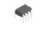
SOP-8
APPLICATIONS
•
•
•
•
•
Wireless Base Station Control Circuits
Optical Network Control Circuits
Instrumentation
Sensors and Controls
Precision Filters
DIP-8
DESCRIPTION
ORDERING INFORMATION
The OP07 is a very low offset and long-term stability
operational amplifier.
Low offset and long-term
stability are achieved by means of a low-noise, bipolarinput-transistor amplifier circuit. For most applications,
external components are not required for offset nulling
and frequency compensation. The true differential
input, with a wide input voltage range and outstanding
common-mode rejection, provides maximum flexibility
and performance in high-noise environments and in
noninverting applications. Low bias currents and
extremely high input impedances are maintained over
the entire temperature range.
The accuracy and stability of the OP07, even at high
gain, combined with the freedom from external nulling
have made the OP07 an industry standard for
instrumentation applications.
Device
Package
OP07D
SOP-8
OP07N
DIP-8
ABSOLUTE MAXIMUM RATINGS
CHARACTERISTIC
Supply Voltage
Input Voltage
SYMBOL
(Note 1)
(Note 2)
Differential Input Voltage
MIN.
MAX.
UNIT
VCC
± 22
V
VIN
± 22
V
± 30
V
(Note 3)
Operating Ambient Temperature Range
TA
-55
125
°C
Junction Temperature
TJ
-40
150
°C
Note 1. All voltage values, unless otherwise noted, are with respect to the midpoint between VCC+ and VCC–.
Nov. 2019 – Rev 1.1
1/9
HTC
�Precision Operational Amplifier
OP07
Note 2. For supply voltages less than ±22 V, the absolute maximum input voltage is equal to the supply voltage.
Note 3. Differential voltages are at IN+ with respect to IN–.
RECOMMENDED OPERATING CONDITIONS
CHARACTERISTIC
SYMBOL
MIN.
MAX.
UNIT
Supply Voltage
VCC
±3
± 18
V
Common Mode Input Voltage (VCC=±15V)
VIC+
-13
13
V
Operating Ambient Temperature Range
TA-
-40
85
V
ORDERING INFORMATION
Package
Order No.
Description
Supplied As
Status
SOP-8
OP07D
Precision Operational Amplifier
Reel
Active
DIP-8
OP07N
Precision Operational Amplifier
Tube
Active
Nov. 2019 – Rev 1.1
2/9
HTC
�Precision Operational Amplifier
OP07
PIN CONFIGURATION
OFFSET N1 1
8
OFFSET N2
IN1(-) 2
7
VCC+
IN1(+) 3
6
OUT
VCC- 4
5 N.C.
SOP-8 / DIP-8
PIN DESCRIPTION
Pin No.
Pin Name
Pin Function
SOP-8
DIP-8
1
1
OFFSET N1
2
2
IN-
Inverting Input
3
3
IN+
Non-Inverting Input
4
4
VCC-
Negative Supply
5
5
N.C.
No Connection
6
6
OUT
Output
7
7
VCC+
Positive Supply
8
8
OFFSET N2
Nov. 2019 – Rev 1.1
External Input Offset Voltage Adjustment
External Input Offset Voltage Adjustment
3/9
HTC
�Precision Operational Amplifier
OP07
FUNCTIONAL BLOCK DIAGRAM
Nov. 2019 – Rev 1.1
4/9
HTC
�Precision Operational Amplifier
OP07
ELECTRICAL CHARACTERISTICS
Specifications with standard type face are for TA = 25°C, VCC = ±15V, and those with boldface type are for -40°C to 85°C
(Note 4)
unless otherwise noted.
PARAMETER
SYMBOL
TEST CONDITIONS
MIN
TYP
MAX
UNIT
VIO
-
60
85
150
250
µV
Input Offset Voltage Drift
without External Trim
TCVIO
-
0.5
1.8
Input Offset Voltage Drift
with External Trim
TCVION
0.5
1.8
INPUT CHARACTERISTICS
Input Offset Voltage
(Note 5)
Long Term Input Offset Voltage
(Note 6)
Stability
RP=20kΩ (See Figure 1)
-
ΔVIO/Time
-
0.4
IIO
-
0.5
1.1
3.8
6.1
TCIIO
-
8
35
IB
-
±1.2
±1.7
±4.0
±6.5
Input Bias Current Drift
TCIB
-
13
35
Input Noise Voltage
enP-P
Input Offset Current
Input Offset Current Drift
Input Bias Current
Input Noise Voltage Density
Input Noise Current
Input Noise Current Density
en
InP-P
In
µV/°C
µV/°C
µV/Month
F = 0.1Hz to 10Hz
-
0.35
0.6
F = 10Hz
-
10.3
18.0
F = 100Hz
-
10.0
13.0
F = 1kHz
-
9.6
11.0
F = 0.1Hz to 10Hz
-
14
30
F = 10Hz
-
0.32
0.80
F = 100Hz
-
0.14
0.23
F = 1kHz
-
0.12
0.17
nA
pA/°C
nA
pA/°C
µVP-P
nV/√Hz
pAP-P
pA/√Hz
Input Resistance
RIN
15
50
-
MΩ
Input Voltage Range
VIR
±13
±13
±14
±13.5
-
V
106
103
123
123
-
dB
-
5
8
20
38
µV/V
Common Mode Rejection Ratio
CMRR
VCM = ±13V
Power Supply Rejection Ratio
PSRR
VCC = ±3V to ±18V
Nov. 2019 – Rev 1.1
5/9
HTC
�Precision Operational Amplifier
OP07
ELECTRICAL CHARACTERISTICS (Continued)
PARAMETER
Large Signal Voltage Gain
SYMBOL
AVO
TEST CONDITIONS
MIN
TYP
MAX
RL ≥ 2kΩ, VO = ±10V
200
150
500
400
-
RL ≥ 500Ω, VO = ±0.5V,
VCC = ±3V
150
400
-
RL ≥ 10kΩ
±12.5
±13.0
-
RL ≥ 2kΩ
±12.0
±11.0
±12.8
±12.6
RL ≥ 1kΩ
±10.5
±12.0
UNIT
V/mV
OUTPUT CHARACTERISTICS
Output Voltage Swing
VO
V
DYNAMIC PERFORMANCE
Open Loop Output Resistance
Power Dissipation
RO
VO = 0, IO = 0
60
VCC = ±15V, No Load
75
Ω
120
mW
PD
VCC = ±3V, No Load
4
RP=20kΩ (See Figure 1)
Offset Adjustment Range
6
±4
mV
Slew Rate
SR
RL ≥ 2kΩ
0.1
0.3
V/µs
Closed Loop Bandwidth
BW
AVOL=1
0.4
0.6
MHz
Note 4. All characteristics are measured under open-loop conditions with zero common-mode input voltage unless otherwise
noted.
Note 5. Input offset voltage measurements are performed by automated test equipment approximately 0.5 seconds after
application of power.
Note 6. Long-term input offset voltage stability refers to the averaged trend time of VIO vs. the time over extended periods
after the first 30 days of operation. Excluding the initial hour of operation, changes in VIO during the first 30 operating
days are typically 2.5 μV.
Nov. 2019 – Rev 1.1
6/9
HTC
�Precision Operational Amplifier
OP07
TYPICAL APPLICATION INFORMATION
The input offset voltage of operational amplifiers (op amps) arises from unavoidable mismatches in the differential
input stage of the op-amp circuit caused by mismatched transistor pairs, collector currents, current gain betas (β),
collector or emitter resistors, etc. The input offset pins allow the designer to adjust for these mismatches by
external circuitry. These input mismatches can be adjusted by putting resistors or a potentiometer between the
inputs as shown in Figure 1. A potentiometer can be used to fine tune the circuit during testing or for
applications which require precision offset control.
Fig 1. Input Offset Voltage Null Circuit
Nov. 2019 – Rev 1.1
7/9
HTC
�Precision Operational Amplifier
OP07
TYPICAL OPERATING CHARACTERISTICS
T.B.D.
Nov. 2019 – Rev 1.1
8/9
HTC
�Precision Operational Amplifier
OP07
REVISION NOTICE
The description in this data sheet is subject to change without any notice to describe its electrical characteristics
properly.
Nov. 2019 – Rev 1.1
9/9
HTC
�
很抱歉,暂时无法提供与“OP07D”相匹配的价格&库存,您可以联系我们找货
免费人工找货- 国内价格
- 1+1.14399
- 30+1.10399
- 100+1.02399
- 500+0.94399
- 1000+0.90399


 工商网监
湘ICP备2023018690号
工商网监
湘ICP备2023018690号
