Bulletin PD-20266 rev. B 02/01
19TQ015 19TQ015S
SCHOTTKY RECTIFIER 19 Amp
IF(AV) = 19Amp VR = 15V
Major Ratings and Characteristics Characteristics
IF(AV) Rectangular waveform VRRM IFSM VF TJ @ tp = 5 µs sine @ 19 Apk, TJ = 75°C range
Description/Features Units
A V A V °C The 19TQ015 Schottky rectifier has been optimized for ultra low forward voltage drop specifically for the OR-ing of parallel power supplies. The proprietary barrier technology allows for reliable operation up to 125° C junction temperature. Typical applications are in parallel switching power supplies, converters, reverse battery protection, and redundant power subsystems. 125°C TJ operation (VR < 5V) Optimized for OR-ing applications Ultra low forward voltage drop High frequency operation Guard ring for enhanced ruggedness and long term reliability High purity, high temperature epoxy encapsulation for enhanced mechanical strength and moisture resistance
19TQ015
19 15 700 0.32 - 55 to 125
Case Styles 19TQ015 19TQ015S
TO-220
D2PAK
www.irf.com
1
�19TQ015/ 19TQ015S
Bulletin PD-20266 rev. B 02/01
Voltage Ratings
Part number
VR Max. DC Reverse Voltage (V) VRWM Max. Working Peak Reverse Voltage (V)
19TQ015
15
Absolute Maximum Ratings
Parameters
IF(AV) Max. Average Forward Current * See Fig. 5 IFSM EAS IAR Max. Peak One Cycle Non-Repetitive Surge Current * See Fig. 7 Non-Repetitive Avalanche Energy Repetitive Avalanche Current
19TQ
19 700 330 6.75 1.50
Units
A
Conditions
50% duty cycle @ TC = 80° C, rectangular wave form 5µs Sine or 3µs Rect. pulse 10ms Sine or 6ms Rect. pulse Following any rated load condition and with rated VRRM applied
A mJ A
TJ = 25 °C, IAS = 1.50 Amps, L = 6 mH Current decaying linearly to zero in 1 µsec Frequency limited by TJ max. VA = 3 x VR typical
Electrical Specifications
Parameters
VFM Max. Forward Voltage Drop * See Fig. 1 (1)
19TQ
0.36 0.46 0.32 0.43
Units
V V V V mA mA mA mA pF nH V/ µs @ 19A @ 38A @ 19A @ 38A TJ = 25 °C TJ = 100 °C
Conditions
TJ = 25 °C TJ = 75 °C VR = rated VR
IRM
Max. Reverse Leakage Current (1) * See Fig. 2
10.5 522 465 285
TJ = 100 °C, VR = 12V TJ = 100 °C, VR = 5V VR = 5VDC, (test signal range 100Khz to 1Mhz) 25 °C Measured lead to lead 5mm from package body
CT LS
Max. Junction Capacitance Typical Series Inductance
2000 8.0 10,000
dv/dt Max. Voltage Rate of Change (Rated VR)
Thermal-Mechanical Specifications
Parameters
TJ Tstg Max. Junction Temperature Range Max. Storage Temperature Range
(1) Pulse Width < 300µs, Duty Cycle < 2%
19TQ
-55 to 125 -55 to 150 1.50 0.50 2 (0.07) Min. Max. 6 (5) 12 (10)
Units
°C °C °C/W °C/W g (oz.) Kg-cm (Ibf-in) DCoperation
Conditions
RthJC Max. Thermal Resistance Junction to Case RthCS Typical Thermal Resistance, Case to Heatsink wt T Approximate Weight MountingTorque
* See Fig. 4
Mounting surface , smooth and greased
2
www.irf.com
�19TQ015/ 19TQ015S
Bulletin PD-20266 rev. B 02/01
10 00 10 00 T =1 0 C 0° J R v rs C rre t - I (m ) ee e u n A R 10 0 7° 5C 5° 0C 2° 5C 1
1 0
10 0
In ta ta e u F r a dC rr n - IF ( ) s n n o s ow r u e t A
.1 0 1 0 T =1 0C 0° J T= 7 ° 5C J T= 2 ° 5C J J n tio C p c n e- C (p ) u c n a a ita c F T
5
1 0
5 1
R v rs V lta e- V (V ee e o g R)
Fig. 2 - Typical Values of Reverse Current Vs. Reverse Voltage
100 00
T =2 ° 5C J
1
10 00
.1 0
.2
.4
.6
.8
1
1 .2
1 .4
10 0 0
5
1 0
1 5
2 0
2 5
3 0
F rw rdV lta eD p- V (V oa o g ro ) F M
R v rs V lta e- V (V ee e o g R)
Fig. 1 - Maximum Forward Voltage Drop Characteristics
1 0 T e a Im e a c - Zth C (° /W h rm l p d n e C) J
Fig. 3 - Typical Junction Capacitance Vs. Reverse Voltage
1
.1
D=0 0 .5 D=0 3 .3 D=0 5 .2 D=0 7 .1 D=0 8 .0
PM D
t 1 t2 N te : os 1 D tyfa to D= t1/ t 2 .u cr 2 P a T =P xZ . ek +T JD M th C C J .0 1 .1 1 1 0 10 0
.0 1 S g P ls in le u e (T e a R s ta c ) h rm l e is n e .0 1 0 .0 0 1 00 .0 0 01 .0 1 0
t1, R c n u r P ls D ra n(S c n s e ta g la u e u tio eod)
Fig. 4 - Maximum Thermal Impedance ZthJC Characteristics
www.irf.com
3
�19TQ015/ 19TQ015S
Bulletin PD-20266 rev. B 02/01
15 0 A w b C s T m e tu - (° ) llo a le a e e p ra re C 1T 05 9 Q1 Rth C (D ) =1 0 C C .5 ° /W J 1 0 D=0 8 .0 D=0 7 .1 .2 8 D=0 5 D=0 3 .3 D=0 0 .5 6 R SL it M im 4 D C
10 0
9 5
9 0
D C
8 5
A e g P w r L s - (W tts v ra e o e o s a)
2
8 0 0
5
1 0
1 5
2 0
2 5
3 0
0 0
4
8
1 2
1 6
2 0
2 4
8 2
A e g F rw rdC rre t - IF V (A v ra e o a un (A ) )
A e g F rw rdC rre t - I v ra e o a un (A ) FV (A )
Fig. 5 - Maximum Allowable Case Temperature Vs. Average Forward Current
1000 (A)
Fig. 6 - Forward Power Loss Characteristics
Non-Repetitive Surge Current - I
FSM
At Any Rated Load Condition And With Rated VRRM Applied Following Surge
100 10
100
1000
10000
Square Wave Pulse Duration - t p (microsec)
Fig. 7 - Maximum Non-Repetitive Surge Current
L H IG H-SPE ED S W ITC H FR EE-W H E EL D IO D E 40H FL40 S02 V d = 25 V olt
D UT
IRFP460 Rg = 25 ohm
+
C URRE NT M O N ITO R
Fig. 8 - Unclamped Inductive Test Circuit
4
www.irf.com
�19TQ015/ 19TQ015S
Bulletin PD-20266 rev. B 02/01
Outline Table
10.54 (0.41) MAX. 3.78 (0.15) 3.54 (0.14) 15.24 (0.60) 14.84 (0.58) 1 14.09 (0.55) 13.47 (0.53) 3 3.96 (0.16) 3.55 (0.14) 2.04 (0.080) MAX. 1.40 (0.05) 1.15 (0.04) 0.94 (0.04) 0.69 (0.03) 2.89 (0.11) 2.64 (0.10) 0.10 (0.004) 2.92 (0.11) 2.54 (0.10) TERM 2 DIA. 6.48 (0.25) 6.23 (0.24) 2° 1.32 (0.05) 1.22 (0.05)
Base Cathode
1 4.57 (0.18) 4.32 (0.17)
3
0.61 (0.02) MAX.
1
3
Cathode
5.08 (0.20) REF.
Anode
Conform to JEDEC outline TO-220AC Dimensions in millimeters and (inches)
10.16 (0.40) REF.
4.69 (0.18) 4.20 (0.16)
1.32 (0.05)
6.47 (0.25)
15.49 (0.61)
1.22 (0.05)
93°
6.18 (0.24)
14.73 (0.58)
2.61 (0.10)
2.32 (0.09) 8.89 (0.35)
5.28 (0.21) 4.78 (0.19)
0.55 (0.02) 0.46 (0.02)
3X
1.40 (0.055)
REF.
0.93 (0.37) 0.69 (0.27)
1.14 (0.045) 2X
MINIMUM RECOMMENDED FOOTPRINT
11.43 (0.45)
Base Cathode
2
1
3
4.57 (0.18)
4.32 (0.17)
2 0.61 (0.02) MAX. 5.08 (0.20) REF.
8.89 (0.35)
17.78 (0.70) 3.81 (0.15)
2.08 (0.08) 2X
1
3
N/C
Anode
2.54 (0.10) 2X
Conform to JEDEC outline D Pak (SMD-220) Dimensions in millimeters and (inches)
2
www.irf.com
5
�19TQ015/ 19TQ015S
Bulletin PD-20266 rev. B 02/01
Ordering Information Table
Device Code
19
1
T
2
Q
3
015
4
S
5
1 2 3 4 5
-
Essential Part Number T = TO-220 Q = Schottky Q Series Voltage Rating (015 = 15V) S = D2Pak
IR WORLD HEADQUARTERS: 2 33 Kansas St., El Segundo, California 90245, USA Tel: (310) 252-7105 TAC Fax: (310) 252-7309 Visit us at www.irf.com for sales contact information. 0 2 /01
6
www.irf.com
�
很抱歉,暂时无法提供与“19TQ015”相匹配的价格&库存,您可以联系我们找货
免费人工找货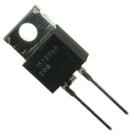


 工商网监
湘ICP备2023018690号
工商网监
湘ICP备2023018690号
