PD- 94829
SMPS MOSFET
Applications l Switch Mode Power Supply ( SMPS ) l Uninterruptable Power Supply l High speed power switching l Lead-Free Benefits l Low Gate Charge Qg results in Simple Drive Requirement l Improved Gate, Avalanche and dynamic dv/dt Ruggedness l Fully Characterized Capacitance and Avalanche Voltage and Current l Effective Coss Specified (See AN1001)
IRF840APbF
HEXFET® Power MOSFET
VDSS
500V
Rds(on) max
0.85 Ω
ID
8.0A
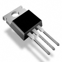
TO-220AB
G DS
Absolute Maximum Ratings
Parameter
ID @ TC = 25°C ID @ TC = 100°C IDM PD @TC = 25°C VGS dv/dt TJ TSTG Continuous Drain Current, VGS @ 10V Continuous Drain Current, VGS @ 10V Pulsed Drain Current Power Dissipation Linear Derating Factor Gate-to-Source Voltage Peak Diode Recovery dv/dt Operating Junction and Storage Temperature Range Soldering Temperature, for 10 seconds Mounting torqe, 6-32 or M3 screw
Max.
8.0 5.1 32 125 1.0 ± 30 5.0 -55 to + 150 300 (1.6mm from case ) 10 lbf•in (1.1N•m)
Units
A W W/°C V V/ns °C
Typical SMPS Topologies:
l l l
Two Transistor Forward Haft Bridge Full Bridge 1
11/11/03
www.irf.com
�IRF840APbF
Static @ TJ = 25°C (unless otherwise specified)
Parameter Min. Drain-to-Source Breakdown Voltage 500 ∆V(BR)DSS/∆TJ Breakdown Voltage Temp. Coefficient ––– RDS(on) Static Drain-to-Source On-Resistance ––– VGS(th) Gate Threshold Voltage 2.0 ––– IDSS Drain-to-Source Leakage Current ––– Gate-to-Source Forward Leakage ––– IGSS Gate-to-Source Reverse Leakage ––– V(BR)DSS Typ. ––– 0.58 ––– ––– ––– ––– ––– ––– Max. Units Conditions ––– V VGS = 0V, ID = 250µA ––– V/°C Reference to 25°C, I D = 1mA 0.85 Ω VGS = 10V, ID = 4.8A 4.0 V VDS = VGS, ID = 250µA 25 VDS = 500V, VGS = 0V µA 250 VDS = 400V, VGS = 0V, TJ = 125°C 100 VGS = 30V nA -100 VGS = -30V
Dynamic @ TJ = 25°C (unless otherwise specified)
gfs Qg Qgs Qgd td(on) tr td(off) tf Ciss Coss Crss Coss Coss Coss eff. Parameter Forward Transconductance Total Gate Charge Gate-to-Source Charge Gate-to-Drain ("Miller") Charge Turn-On Delay Time Rise Time Turn-Off Delay Time Fall Time Input Capacitance Output Capacitance Reverse Transfer Capacitance Output Capacitance Output Capacitance Effective Output Capacitance Min. 3.7 ––– ––– ––– ––– ––– ––– ––– ––– ––– ––– ––– ––– ––– Typ. ––– ––– ––– ––– 11 23 26 19 1018 155 8.0 1490 42 56 Max. Units Conditions ––– S VDS = 50V, ID = 4.8A 38 ID = 8.0A 9.0 nC VDS = 400V 18 VGS = 10V, See Fig. 6 and 13 ––– VDD = 250V ––– ID = 8.0A ns ––– RG = 9.1Ω ––– R D = 31Ω,See Fig. 10 ––– VGS = 0V ––– VDS = 25V ––– pF ƒ = 1.0MHz, See Fig. 5 ––– VGS = 0V, VDS = 1.0V, ƒ = 1.0MHz ––– VGS = 0V, VDS = 400V, ƒ = 1.0MHz ––– VGS = 0V, VDS = 0V to 400V
Avalanche Characteristics
Parameter
EAS IAR EAR Single Pulse Avalanche Energy Avalanche Current Repetitive Avalanche Energy
Typ.
––– ––– –––
Max.
510 8.0 13
Units
mJ A mJ
Thermal Resistance
RθJC RθCS RθJA
Parameter
Junction-to-Case Case-to-Sink, Flat, Greased Surface Junction-to-Ambient Parameter Continuous Source Current (Body Diode) Pulsed Source Current (Body Diode) Diode Forward Voltage Reverse Recovery Time Reverse RecoveryCharge Forward Turn-On Time
Typ.
––– 0.50
Max.
1.0 ––– 62
Units
°C/W
Diode Characteristics
Min. Typ. Max. Units IS
I SM
VSD t rr Q rr ton
Conditions D MOSFET symbol ––– ––– 8.0 showing the A G integral reverse ––– ––– 32 S p-n junction diode. ––– ––– 2.0 V TJ = 25°C, IS = 8.0A, VGS = 0V ––– 422 633 ns TJ = 25°C, IF = 8.0A ––– 2.16 3.24 µC di/dt = 100A/µs Intrinsic turn-on time is negligible (turn-on is dominated by LS+LD)
2
www.irf.com
�IRF840APbF
100
VGS 15V 10V 8.0V 7.0V 6.0V 5.5V 5.0V BOTTOM 4.5V TOP
100
I D , Drain-to-Source Current (A)
I D , Drain-to-Source Current (A)
10
10
VGS 15V 10V 8.0V 7.0V 6.0V 5.5V 5.0V BOTTOM 4.5V TOP
4.5V
1
1
4.5V
20µs PULSE WIDTH TJ = 25 °C
1 10 100
0.1 0.1
VDS, Drain-to-Source Voltage (V)
0.1 0.1
20µs PULSE WIDTH TJ = 150 °C
1 10 100
VDS , Drain-to-Source Voltage (V)
Fig 1. Typical Output Characteristics
Fig 2. Typical Output Characteristics
100
3.0
RDS(on) , Drain-to-Source On Resistance (Normalized)
8.0 ID = 7.4A
I D , Drain-to-Source Current (A)
2.5
10
TJ = 150 ° C
2.0
TJ = 25 ° C
1
1.5
1.0
0.5
0.1 4.0
V DS = 50V 20µs PULSE WIDTH 5.0 6.0 7.0 8.0 9.0
0.0 -60 -40 -20
VGS = 10V
0 20 40 60 80 100 120 140 160
VGS , Gate-to-Source Voltage (V)
TJ , Junction Temperature ( °C)
Fig 3. Typical Transfer Characteristics
Fig 4. Normalized On-Resistance Vs. Temperature
www.irf.com
3
�IRF840APbF
100000 VGS = 0V, f = 1 MHZ Ciss = C + Cgd, C gs ds SHORTED Crss = C gd Coss = C + Cgd ds
20
8.0 ID = 7.4 A
VGS , Gate-to-Source Voltage (V)
10000
16
VDS = 400V VDS = 250V VDS = 100V
C, Capacitance(pF)
1000
Ciss Coss
12
100
8
10
Crss
4
1 1 10 100 1000
0
FOR TEST CIRCUIT SEE FIGURE 13
0 10 20 30 40
VDS , Drain-to-Source Voltage (V)
QG , Total Gate Charge (nC)
Fig 5. Typical Capacitance Vs. Drain-to-Source Voltage
Fig 6. Typical Gate Charge Vs. Gate-to-Source Voltage
100
100
ISD , Reverse Drain Current (A)
OPERATION IN THIS AREA LIMITED BY RDS(on)
10us
10
TJ = 150 ° C
ID , Drain Current (A)
10
100us
1ms 1
1
TJ = 25 ° C
10ms
0.1 0.2
V GS = 0 V
0.5 0.8 1.1 1.4
0.1
TC = 25 °C TJ = 150 °C Single Pulse
10 100 1000 10000
VSD ,Source-to-Drain Voltage (V)
VDS , Drain-to-Source Voltage (V)
Fig 7. Typical Source-Drain Diode Forward Voltage
Fig 8. Maximum Safe Operating Area
4
www.irf.com
�IRF840APbF
8.0
V DS V GS
RD
ID , Drain Current (A)
6.0
RG 10V
D.U.T.
+
-V DD
4.0
Pulse Width ≤ 1 µs Duty Factor ≤ 0.1 %
2.0
Fig 10a. Switching Time Test Circuit
VDS 90%
0.0
25
50
75
100
125
150
TC , Case Temperature ( °C)
Fig 9. Maximum Drain Current Vs. Case Temperature
10% VGS
td(on) tr t d(off) tf
Fig 10b. Switching Time Waveforms
10
Thermal Response (Z thJC )
1 D = 0.50 0.20 0.1 0.10 0.05 0.02 0.01 0.01 0.00001 PDM t1 t2 SINGLE PULSE (THERMAL RESPONSE) 0.0001 0.001 0.01 Notes: 1. Duty factor D = t 1 / t 2 2. Peak T J = P DM x Z thJC + TC 0.1 1
t1 , Rectangular Pulse Duration (sec)
Fig 11. Maximum Effective Transient Thermal Impedance, Junction-to-Case
www.irf.com
5
�IRF840APbF
EAS , Single Pulse Avalanche Energy (mJ)
15V
1200
TOP BOTTOM
1000
VDS
L
DRIVER
ID 3.6A 5.1A 8.0A
800
RG
20V
D.U.T
IAS tp
+ V - DD
A
600
0.01Ω
Fig 12a. Unclamped Inductive Test Circuit
V(BR)DSS tp
400
200
0
25
50
75
100
125
150
Starting TJ , Junction Temperature ( °C)
I AS
Fig 12b. Unclamped Inductive Waveforms
QG
Fig 12c. Maximum Avalanche Energy Vs. Drain Current
10 V
QGS
QGD
V DSav , Avalanche Voltage ( V )
600
VG
580
Charge
Fig 13a. Basic Gate Charge Waveform
Current Regulator Same Type as D.U.T.
560
50KΩ 12V .2µF .3µF
540
D.U.T. VGS
3mA
+ V - DS
520 0.0 1.0 2.0 3.0 4.0 5.0 6.0 7.0 8.0
IAV , Avalanche Current ( A)
IG ID
Current Sampling Resistors
Fig 13b. Gate Charge Test Circuit
Fig 12d. Typical Drain-to-Source Voltage Vs. Avalanche Current
6
www.irf.com
�IRF840APbF
Peak Diode Recovery dv/dt Test Circuit
D.U.T
+
+
Circuit Layout Considerations • Low Stray Inductance • Ground Plane • Low Leakage Inductance Current Transformer
-
+
RG • • • • dv/dt controlled by RG Driver same type as D.U.T. ISD controlled by Duty Factor "D" D.U.T. - Device Under Test
+ V DD
Driver Gate Drive P.W. Period D=
P.W. Period VGS=10V
*
D.U.T. ISD Waveform Reverse Recovery Current Body Diode Forward Current di/dt D.U.T. VDS Waveform Diode Recovery dv/dt
VDD
Re-Applied Voltage Inductor Curent
Body Diode
Forward Drop
Ripple ≤ 5%
ISD
* VGS = 5V for Logic Level Devices Fig 14. For N-Channel HEXFETS
www.irf.com
7
�IRF840APbF
TO-220AB Package Outline
2.87 (.113) 2.62 (.103) 10.54 (.415) 10.29 (.405) 3.78 (.149) 3.54 (.139) -A6.47 (.255) 6.10 (.240) -B4.69 (.185) 4.20 (.165) 1.32 (.052) 1.22 (.048)
4 15.24 (.600) 14.84 (.584)
1.15 (.045) MIN 1 2 3
LEAD ASSIGNMENTS IGBTs, CoPACK 1 - GATE 21- GATE DRAIN 1- GATE 32- DRAINSOURCE 2- COLLECTOR 3- SOURCE 3- EMITTER 4 - DRAIN
LEAD ASSIGNMENTS
HEXFET
14.09 (.555) 13.47 (.530)
4- DRAIN
4.06 (.160) 3.55 (.140)
4- COLLECTOR
3X 3X 1.40 (.055) 1.15 (.045)
0.93 (.037) 0.69 (.027) M BAM
3X
0.55 (.022) 0.46 (.018)
0.36 (.014)
2.54 (.100) 2X NOTES: 1 DIMENSIONING & TOLERANCING PER ANSI Y14.5M, 1982. 2 CONTROLLING DIMENSION : INCH
2.92 (.115) 2.64 (.104)
3 OUTLINE CONFORMS TO JEDEC OUTLINE TO-220AB. 4 HEATSINK & LEAD MEASUREMENTS DO NOT INCLUDE BURRS.
TO-220AB Part Marking Information
E XAMPLE : T H IS IS AN IRF 1010 LOT CODE 1789 AS S E MB L E D ON WW 19, 1997 IN T H E AS S E MB LY L INE "C" INT E R NAT IONAL R E CT IF IE R L OGO AS S E MB LY L OT CODE PAR T NU MB E R
Note: "P" in assembly line position indicates "Lead-Free"
DAT E CODE YE AR 7 = 1997 WE E K 19 L INE C
Notes: max. junction temperature. ( See fig. 11 ) Starting TJ = 25°C, L = 16 mH RG = 25Ω, IAS = 8.0A. (See Figure 12) ISD ≤ 8.0A, di/dt ≤ 100A/µs, VDD ≤ V(BR)DSS, TJ ≤ 150°C
Repetitive rating; pulse width limited by
Pulse width ≤ 300µs; duty cycle ≤ 2%.
Coss eff. is a fixed capacitance that gives the same charging time
as Coss while VDS is rising from 0 to 80% VDSS
Data and specifications subject to change without notice.
IR WORLD HEADQUARTERS: 233 Kansas St., El Segundo, California 90245, USA Tel: (310) 252-7105 TAC Fax: (310) 252-7903 Visit us at www.irf.com for sales contact information. 11/03
8
www.irf.com
�


 工商网监
湘ICP备2023018690号
工商网监
湘ICP备2023018690号
