DSS25-0025B
Schottky Diode
VRRM
=
25 V
I FAV
=
25 A
VF
=
0.45 V
High Performance Schottky Diode
Low Loss and Soft Recovery
Single Diode
Part number
DSS25-0025B
Backside: cathode
3
1
Features / Advantages:
Applications:
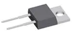
Package: TO-220
● Very low Vf
● Extremely low switching losses
● Low Irm values
● Improved thermal behaviour
● High reliability circuit operation
● Low voltage peaks for reduced
protection circuits
● Low noise switching
● Rectifiers in switch mode power
supplies (SMPS)
● Free wheeling diode in low voltage
converters
● Industry standard outline
● RoHS compliant
● Epoxy meets UL 94V-0
Disclaimer Notice
Information furnished is believed to be accurate and reliable. However, users should independently
evaluate the suitability of and test each product selected for their own applications. Littelfuse products are not designed for,
and may not be used in, all applications. Read complete Disclaimer Notice at www.littelfuse.com/disclaimer-electronics.
IXYS reserves the right to change limits, conditions and dimensions.
© 2021 IXYS all rights reserved
Data according to IEC 60747and per semiconductor unless otherwise specified
20211013c
�DSS25-0025B
Ratings
Schottky
Conditions
Symbol
VRSM
Definition
max. non-repetitive reverse blocking voltage
TVJ = 25°C
VRRM
max. repetitive reverse blocking voltage
TVJ = 25°C
25
V
IR
reverse current, drain current
VF
forward voltage drop
I FAV
average forward current
VF0
threshold voltage
rF
slope resistance
R thJC
thermal resistance junction to case
min.
VR =
25 V
TVJ = 25°C
20
mA
25 V
TVJ = 100°C
80
mA
TVJ = 25°C
0.52
V
0.67
V
0.45
V
IF =
25 A
IF =
50 A
IF =
25 A
IF =
50 A
TVJ = 125 °C
TC = 125 °C
0.66
V
T VJ = 150 °C
25
A
TVJ = 150 °C
0.21
V
8.8
mΩ
d = 0.5
for power loss calculation only
1.4 K/W
R thCH
thermal resistance case to heatsink
Ptot
total power dissipation
I FSM
max. forward surge current
t = 10 ms; (50 Hz), sine; VR = 0 V
TVJ = 45°C
CJ
junction capacitance
VR =
TVJ = 25°C
EAS
non-repetitive avalanche energy
I AS =
I AR
repetitive avalanche current
VA = 1.5·V R typ. f = 10 kHz
© 2021 IXYS all rights reserved
max. Unit
25
V
VR =
rectangular
IXYS reserves the right to change limits, conditions and dimensions.
typ.
K/W
0.5
TC = 25°C
5 V f = 1 MHz
20 A
L = 100 µH
90
330
1.26
TVJ = 25 °C
Data according to IEC 60747and per semiconductor unless otherwise specified
W
A
nF
60
mJ
2
A
20211013c
�DSS25-0025B
Package
Ratings
TO-220
Symbol
I RMS
Definition
Conditions
RMS current
per terminal
min.
TVJ
virtual junction temperature
T op
operation temperature
Tstg
storage temperature
-55
typ.
max.
35
Unit
A
-55
150
°C
-55
125
°C
150
°C
2
Weight
MD
mounting torque
FC
mounting force with clip
g
0.4
0.6
Nm
20
60
N
Product Marking
Part Number
Logo
Date Code
Lot #
XXXXXX
yywwZ
123456
Location
Ordering
Standard
Ordering Number
DSS25-0025B
Equivalent Circuits for Simulation
I
V0
R0
Marking on Product
DSS25-0025B
* on die level
Delivery Mode
Tube
Code No.
475114
T VJ = 150°C
Schottky
V 0 max
threshold voltage
0.21
V
R0 max
slope resistance *
5.6
mΩ
IXYS reserves the right to change limits, conditions and dimensions.
© 2021 IXYS all rights reserved
Quantity
50
Data according to IEC 60747and per semiconductor unless otherwise specified
20211013c
�DSS25-0025B
Outlines TO-220
A
= supplier option
H1
ØP
D
4
3
L1
1
L
2x b2
2x b
C
e
A2
3
IXYS reserves the right to change limits, conditions and dimensions.
© 2021 IXYS all rights reserved
Millimeter
Min.
Max.
Inches
Min.
Max.
A
A1
A2
4.32
1.14
2.29
4.82
1.39
2.79
0.170
0.045
0.090
0.190
0.055
0.110
b
b2
0.64
1.15
1.01
1.65
0.025
0.045
0.040
0.065
C
D
0.35
14.73
0.56
16.00
0.014
0.580
0.022
0.630
E
e
H1
9.91
5.08
5.85
10.66
BSC
6.85
0.390
0.200
0.230
0.420
BSC
0.270
L
L1
12.70
2.79
13.97
5.84
0.500
0.110
0.550
0.230
ØP
Q
3.54
2.54
4.08
3.18
0.139
0.100
0.161
0.125
A1
Q
E
Dim.
1
Data according to IEC 60747and per semiconductor unless otherwise specified
20211013c
�DSS25-0025B
Schottky
40
1000
3000
TVJ = 150°C
100
IF 10
100°C
IR 10
[A]
2000
125°C
TVJ = 25°C
CT
75°C
TVJ =
150°C
125°C
25°C
1
0.0
1000
[mA] 1
[pF]
50°C
0.1
25°C
0.01
0.2
0.4
0.6
500
0
5
10
15
20
25
0
5
10
15
20
25
VF [V]
VR [V]
VR [V]
Fig. 1 Max. forward voltage
drop characteristics
Fig. 2 Typ. reverse current
IR vs. reverse voltage VR
Fig. 3 Typ. junction capacitance
CT vs. reverse voltage VR
40
20
30
d = 0.5
15
DC
P(AV)
IF(AV)
d=
DC
0.5
0.33
0.25
0.17
0.08
10
20
[W]
[A]
10
5
0
0
0
40
80
120
0
160
TC [°C]
10
20
30
IF(AV) [A]
Fig. 4 Average forward current
IF(AV) vs. case temp. TC
Fig. 5 Forward power loss
characteristics
2
1
D=0.5
0.33
0.25
ZthJC
0.17
Single Pulse
0.08
0.1
[K/W]
0.01
0.0001
Note: All curves are per diode
0.001
0.01
0.1
1
10
t [s]
Fig. 6 Transient thermal impedance junction to case at various duty cycles
IXYS reserves the right to change limits, conditions and dimensions.
© 2021 IXYS all rights reserved
Data according to IEC 60747and per semiconductor unless otherwise specified
20211013c
�
很抱歉,暂时无法提供与“DSS25-0025B”相匹配的价格&库存,您可以联系我们找货
免费人工找货- 国内价格 香港价格
- 50+7.1171050+0.86256
- 150+7.08384150+0.85852
- 500+7.08368500+0.85851
- 1000+7.083531000+0.85849
- 2000+7.083372000+0.85847
- 国内价格 香港价格
- 50+7.2522350+0.87893
- 150+7.21834150+0.87483
- 500+7.21819500+0.87481
- 1000+7.218021000+0.87479
- 2000+7.217862000+0.87477


 工商网监
湘ICP备2023018690号
工商网监
湘ICP备2023018690号
