JIANGSU CHANGJING ELECTRONICS TECHNOLOGY CO., LTD
SOT-89-3L Plastic-Encapsulate Voltage Regulator
CJ79L06
Three-terminal negative voltage regulator
SOT-89-3L
FEATURES
Maximum output current
IOM: 0.1A
Output voltage
Vo: -6 V
Continuous total dissipation
PD:0.6 W (Ta= 25 ℃ )
1. GND
2. IN
3.OUT
ABSOLUTE MAXIMUM RATINGS (Operating temperature range applies unless otherwise specified)
Parameter
Symbol
Value
Unit
Vi
-30
V
℃/W
Input Voltage
Thermal Resistance from Junction to Ambient
RθJA
208.3
Operating Junction Temperature Range
TOPR
-40~+125
Storage Temperature Range
TSTG
-65~+150
℃
℃
ELECTRICAL CHARACTERISTICS AT SPECIFIED VIRTUAL JINCTION TEMPERATURE (VI=-11V,Io=40mA,Ci=0.33 μF,Co=0.1μF, unless otherwise specified)
Parameter
Output Voltage
Load Regulation
Min
Typ
Max
Unit
TJ=25℃
-5.82
-6.0
-6.18
V
-8V≤Vl≤-20V, Io=1mA~40mA
-5.7
-6.0
-6.3
V
Io=1mA~70mA
-5.7
-6.0
-6.3
V
Io=1mA~100mA ,TJ=25℃
21
80
mV
Io=1mA~40mA ,TJ=25℃
11
40
mV
-8V≤Vl≤-20V ,TJ=25℃
20
175
mV
-9V≤Vl≤-20V ,TJ=25℃
15
125
mV
TJ=25℃
3.9
6.0
mA
Symbol
Vo
ΔVo
Line Regulation
ΔVo
Quiescent Current
Iq
Test conditions
ΔIq
-9V≤Vl≤-20V
1.5
mA
ΔIq
1mA≤Vl≤40mA
0.1
mA
Output Noise Voltage
VN
10Hz≤f≤100KHz ,TJ=25℃
Ripple Rejection
RR
-9V≤Vl≤-19V,f=120HZ
Dropout Voltage
Vd
TJ=25℃
Quiescent Current Change
40
44
μV/Vo
48
dB
1.7
V
* Pulse test.
TYPICAL APPLICATION
-Vi
2
3
-Vo
CJ79L06
Ci
1
Co
0.1μF
0.33μF
Note: Bypass capacitors are recommended for optimum stability and transient response and should be located as close
possible to the regulators.
www.jscj-elec.com
1
Rev. - 2.2
�Typical Characteristics
Dropout Characteristics
Output Characteristics
-7
-8
TJ=25℃
(V)
-6
-5
-4
-3
-2
IO=0mA
-4
IO=-40mA,-70mA,-100mA
-3
-2
-1
-1
0
-5
VO
-6
OUTPUT VOLTAGE
(V)
OUTPUT VOLTAGE VO
TJ=25℃
IO=0mA
-7
0
-5
-10
-15
-20
INPUT VOLTAGE
VIN
-25
0
-30
-4.0
-4.5
-5.0
-5.5
-6.5
-6.0
INPUT VOLTAGE
(V)
Quiescent Current vs Input Voltage
VIN
-7.0
Current Cut-off Grid Voltage
VIN=-11V
TJ=25℃
-2.5
TJ=25℃
-7
(V)
Pulsed
VO
-2.0
OUTPUT VOLTAGE
IQ
(mA)
IO=0mA
QUIESCENT CURRENT
-8.0
-8
-3.0
-1.5
-1.0
-0.5
0.0
-7.5
(V)
-6
-5
-4
-3
-2
-1
0
-5
-10
-15
-20
INPUT VOLTAGE
VIN
-25
0
-30
0
50
100
150
200
OUTPUT CURRENT
(V)
Output Voltage vs Junction Temperature
IO
250
300
(A)
Power Derating Curve
-8
800
Vin= -11V
OUTPUT VOLTAGE VO (V)
POWER DISSIPATION PD (mW)
IO= 5mA
-7
-6
-5
-4
600
400
200
-3
-2
-40
-25
0
25
50
75
100
0
125
JUNCTION TEMPERATURE TJ (℃ )
www.jscj-elec.com
-40
-25
0
25
50
75
100
125
JUNCTION TEMPERATURE TJ (℃ )
2
Rev. - 2.2
�Dimensions In Millimeters
Max
Min
1.400
1.600
0.320
0.520
0.400
0.580
0.350
0.440
4.400
4.600
1.550 REF.
2.300
2.600
3.940
4.250
1.500 TYP.
3.000 TYP.
0.900
1.200
Symbol
A
b
b1
c
D
D1
E
E1
e
e1
L
www.jscj-elec.com
3
Dimensions In Inches
Max
Min
0.063
0.055
0.013
0.020
0.016
0.023
0.014
0.017
0.173
0.181
0.061 REF.
0.091
0.102
0.155
0.167
0.060 TYP.
0.118 TYP.
0.035
0.047
Rev. - 2.2
�www.jscj-elec.com
4
Rev. - 2.2
�DISCLAIMER
IMPORTANT NOTICE, PLEASE READ CAREFULLY
The information in this data sheet is intended to describe the operation and characteristics of our products.
JSCJ has the right to make any modification, enhancement, improvement, correction or other changes to any
content in this data sheet, including but not limited to specification parameters, circuit design and application
information, without prior notice.
Any person who purchases or uses JSCJ products for design shall: 1. Select products suitable for circuit
application and design; 2. Design, verify and test the rationality of circuit design; 3. Procedures to ensure that
the design complies with relevant laws and regulations and the requirements of such laws and regulations.
JSCJ makes no warranty or representation as to the accuracy or completeness of the information contained
in this data sheet and assumes no responsibility for the application or use of any of the products described in
this data sheet.
Without the written consent of JSCJ, this product shall not be used in occasions requiring high quality or high
reliability, including but not limited to the following occasions: medical equipment, automotive electronics,
military facilities and aerospace. JSCJ shall not be responsible for casualties or property losses caused by
abnormal use or application of this product.
Official Website: www.jscj-elec.com
Copyright © JIANGSU CHANGJING ELECTRONICS TECHNOLOGY CO., LTD.
�
很抱歉,暂时无法提供与“CJ79L06”相匹配的价格&库存,您可以联系我们找货
免费人工找货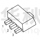


 工商网监
湘ICP备2023018690号
工商网监
湘ICP备2023018690号
