Photocoupler
Product Data Sheet
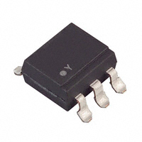
4N25/ 4N26
(M, S, S-TA1)
Spec No.: DS-70-99-0010
Effective Date: 12/11/2015
Revision: C
LITE-ON DCC
RELEASE
BNS-OD-FC001/A4
LITE-ON Technology Corp. / Optoelectronics
No.90,Chien 1 Road, Chung Ho, New Taipei City 23585, Taiwan, R.O.C.
Tel: 886-2-2222-6181 Fax: 886-2-2221-1948 / 886-2-2221-0660
http://www.liteon.com/opto
�Photocoupler
4N2X Series
1. DESCRIPTION
1.1 Features
High Current transfer ratio (CTR : MIN. 10% at IF = 10mA, VCE = 10V )
Response time( ton : TYP. 3s at VCC = 10V, IC = 2mA, RL = 100 )
Input-output isolation voltage
4N25 series : Viso = 2,500Vrms
4N26 series : Viso = 1,500Vrms
4N27 series : Viso = 1,500Vrms
4N28 series : Viso = 500Vrms
Dual-in-line package :
4N25, 4N26, 4N27, 4N28
Wide lead spacing package :
Surface mounting package :
Tape and reel packaging :
Safety approval
4N25M, 4N26M, 4N27M, 4N28M
4N25S, 4N26S, 4N27S, 4N28S
4N25S-TA1, 4N26S-TA1, 4N27S-TA1, 4N28S-TA1
UL approval (NO. E113898)
TUV approval (NO. R9653630)
DEMKO approval (NO. 303985)
CSA & cUL, VDE, FIMKO, CQC approved
RoHS Compliance
All materials be used in device are followed EU RoHS directive (No.2002/95/EC).
ESD pass HBM 8000V/MM2000V
MSL class 1
1.2 Applications
Hybrid substrates that require high density mounting.
Programmable controllers
1/14
Part No. : 4N2X series
BNS-OD-FC002/A4
Rev.: C
�Photocoupler
4N2X Series
2. PACKAGE DIMENSIONS
2.1
4N25
2.3
4N25S
2.2
4N25M
Notes :
1. Year date code.
2. 2-digit work week.
3. Factory identification mark shall be marked
(W: China-CZ, Y: Thailand)
4. VDE option.
Dimensions in millimeters(inches).
2/14
Part No. : 4N2X series
BNS-OD-FC002/A4
Rev.: C
�Photocoupler
4N2X Series
2.4
2.6
4N26
2.5
4N26M
4N26S
Notes :
1. Year date code.
2. 2-digit work week.
3. Factory identification mark shall be marked
(W: China-CZ, Y: Thailand)
4. VDE option.
Dimensions in millimeters(inches).
3/14
Part No. : 4N2X series
BNS-OD-FC002/A4
Rev.: C
�Photocoupler
4N2X Series
2.7
2.9
4N27
2.8
4N27M
4N27S
Notes :
1. Year date code.
2. 2-digit work week.
3. Factory identification mark shall be marked
(W: China-CZ, Y: Thailand)
4. VDE option.
Dimensions in millimeters(inches).
4/14
Part No. : 4N2X series
BNS-OD-FC002/A4
Rev.: C
�Photocoupler
4N2X Series
2.10
2.12
4N28
2.11
4N28M
4N28S
Notes :
1. Year date code.
2. 2-digit work week.
3. Factory identification mark shall be marked
(W: China-CZ, Y: Thailand)
4. VDE option.
Dimensions in millimeters(inches).
5/14
Part No. : 4N2X series
BNS-OD-FC002/A4
Rev.: C
�Photocoupler
4N2X Series
3. TAPING DIMENSIONS
3.1 4N25S-TA , 4N26S-TA , 4N27S-TA , 4N28S-TA
3.2 4N25S-TA1 , 4N26S-TA1 , 4N27S-TA1 , 4N28S-TA1
Description
Symbol
Dimension in mm (inch)
Tape wide
W
16±0.3 (0.63)
Pitch of sprocket holes
P0
4±0.1 (0.15)
F
7.5±0.1 (0.295)
P2
2±0.1 (0.079)
P1
12±0.1 (0.472)
Distance of compartment
Distance of compartment to
compartment
3.3 Quantities Per Reel
Package Type
TA/TA1
Quantities (pcs)
1000
6/14
Part No. : 4N2X series
BNS-OD-FC002/A4
Rev.: C
�Photocoupler
4N2X Series
4. RATING AND CHARACTERISTICS
4.1 Absolute Maximum Ratings at Ta=25°C
Parameter
Input
Output
Symbol
Rating
Unit
Forward Current
IF
80
mA
Reverse Voltage
VR
6
V
Power Dissipation
P
150
mW
Collector - Emitter Voltage
VCEO
30
V
Emitter - Collector Voltage
VECO
7
V
Collector - Base Voltage
VCBO
70
V
Collector Current
IC
100
mA
Collector Power Dissipation
PC
150
mW
Total Power Dissipation
Ptot
250
mW
4N25 series
2,500
4N26 series
*1.
1,500
Viso
*1 Isolation Voltage
Vrms
4N27 series
1,500
4N28 series
500
Operating Temperature
Topr
-55 ~ +100
o
C
Storage Temperature
Tstg
-55 ~ +150
o
C
*2 Soldering Temperature
Tsol
260
o
C
AC For 1 Minute,
R.H. = 40 ~ 60%
Isolation voltage shall be measured using the following method.
(1) Short between anode and cathode on the primary side and between collector and emitter on the
secondary side.
(2) The isolation voltage tester with zero-cross circuit shall be used.
(3) The waveform of applied voltage shall be a sine wave.
*2.
For 10 Seconds
7/14
Part No. : 4N2X series
BNS-OD-FC002/A4
Rev.: C
�Photocoupler
4N2X Series
4.2
Electrical Optical Characteristics at Ta=25°C
Parameter
Input
Symbol
Min.
Typ.
Max.
Unit
Forward Voltage
VF
—
1.2
1.5
V
IF=10mA
Reverse Current
IR
—
—
10
A
VR=4V
Terminal Capacitance
Ct
—
50
—
pF
V=0, f=1KHz
Collector Dark Current
ICEO
—
—
50
nA
VCE=10V, IF=0
BVCEO
30
—
—
V
IC=0.1mA, IF=0
BVECO
7
—
—
V
IE=10A, IF=0
BVCBO
70
—
—
V
IC=0.1mA, IF=0
IC
2
—
—
mA
CTR
20
—
—
%
IC
1
—
—
mA
CTR
10
—
—
%
VCE(sat)
—
0.1
0.5
V
Riso
51010
11011
—
Collector-Emitter
Test Condition
Breakdown Voltage
Output
Emitter-Collector Breakdown
Voltage
Collector-Base Breakdown
Voltage
Collector Current (4N25/4N26)
* Current Transfer Ratio
(4N25/4N26)
IF=10mA, VCE=10V
Collector Current (4N27/4N28)
* Current Transfer Ratio
TRANSFER
CHARACTERISTI
CS
(4N27/4N28)
Collector-Emitter
IF=50mA, IC=2mA
Saturation Voltage
Isolation Resistance
DC500V,
40 ~ 60% R.H.
*.
Floating Capacitance
Cf
—
1
—
pF
40 ~f=1MHz
60% R.H.
V=0,
Response Time (Rise)
tr
—
3
—
s
VCE=2V, IC=2mA
Response Time (Fall)
tf
—
3
—
s
RL=100,
Current Transfer Ratio
CTR
IC
100%
IF
8/14
Part No. : 4N2X series
BNS-OD-FC002/A4
Rev.: C
�Photocoupler
4N2X Series
5. CHARACTERISTICS CURVES
F ig .1 F o rw a rd C u rre n t vs. A m b ie n t
F ig .2 C o lle cto r P o w e r D issip a tio n vs.
T e m p e ra tu re
A m b ie n t T e m p e ra tu re
C o llec to r p o w er d issip atio n Pc (m W)
Fo rw ard c urrent I F (m A)
100
80
60
40
20
0
-55
-25
0
25
50
75
100
125
200
150
100
50
0
-55
-25
25
0
50
75
100
o
Am b ient tem p erature Ta ( C )
F ig .3 F o rw a rd C u rre n t vs. F o rw a rd
F ig .4 C u rre n t T ra n sfe r R a tio vs. F o rw a rd
V o lta g e
C u rre n t
50
500
V = 10V
200
C urrent Transfer ratio C TR (%)
Fo rw ard c urrent I F (m A)
o
o
o
o
100
o
50
20
10
5
2
1
0
0.5
1.0
1.5
2.0
2.5
o
Ta= 25 C
40
30
20
R =
10
100k
0
0.1 0.2
3.0
Fo rw ard vo ltag e V F (V)
5 10 20
50 100
vs. A m b ie n t T e m p e ra tu re
15
300
Pc (M AX.)
30m A
10
20m A
5
10m A
5m A
Relative c urrent transfer ratio (%)
IF = 40m A
o
2
F ig .6 R e la tive C u rre n t T ra n sfe r R a tio
C o lle cto r-e m itte r V o lta g e
Ta= 25 C
0.5 1
Fo rw ard c urrent I F (m A)
F ig .5 C o lle cto r C u rre n t vs.
C o llec to r c urrent Ic (m A)
125
o
Am b ient tem p erature Ta ( C )
I F = 10m A
V = 10V
200
100
0
0
0
5
10
C o llec to r-em itter vo ltag e VC E (V)
15
-55
-25
0
25
50
75
100
o
Am b ient tem p erature Ta ( C )
9/14
Part No. : 4N2X series
BNS-OD-FC002/A4
Rev.: C
�Photocoupler
4N2X Series
F ig .7 C o lle cto r-e m itte r S a tu ra tio n V o lta g e vs.
F ig .8 C o lle cto r D a rk C u rre n t vs.
A m b ie n t T e m p e ra tu re
A m b ie n t T e m p e ra tu re
-6
10
I F = 50m A
I C = 2m A
5
C o llec to r d ark c urrent I C EO (A)
C o llec to r-em itter saturatio n vo ltag e
VC E(sat)(V)
0.3
0.2
0.1
V = 10V
-7
10
5
-8
10
5
-9
10
5
-10
10
5
10
5
-12
10
5
-13
0
-55
10
-25
0
25
50
75
100
-55
-25
0
20
40
60
100 125
O
O
Am b ient tem p erature Ta ( C )
Am b ient tem p erature Ta ( C )
F ig .9 R e sp o n se T im e vs. L o a d R e sista n ce
5
V = 10V
Ic = 2m A
Ta= 25 C
50
tr
O
20
Resp o nse tim e ( s)
V = 5V
Ic = 2m A
Ta= 25 C
tf
O
Vo ltag e g ain Av (d B)
100
F ig .1 0 F re q u e n cy R e sp o n se
td
10
5
2
ts
1
0.5
0
-5
100
R L= 10k
1k
-10
-15
0.2
0.1
0.05
0.1 0.2 0.5 1
2
5 10 20
Lo ad resistanc e R L (k
-20
0.5
50
1
2
5
)
10 20
50 100 200 500
Freq uenc y f (kH z)
F ig .1 1 C o lle cto r-e m itte r S a tu ra tio n
T e st C ircu it fo r R e sp o n se T im e
5
7m A
5m A
3m A
2m A
6
1m A
Vc c
7
Ic = 0.5m A
C o llec to r-em itter saturatio n vo ltag e
VC E( sat)(V)
V o lta g e vs. F o rw a rd C u rre n t
Inp ut
O utp ut
O
Ta= 25 C
Inp ut
RD
RL
10%
O utp ut
90%
ts
td
4
tr
3
tf
T e st C ircu it fo r F re q u e n cy R e sp o n se
2
Vc c
1
RD
RL
O utp ut
0
0
5
10
15
20
25
30
Fo rw ard c urrent I F (m A)
10/14
Part No. : 4N2X series
BNS-OD-FC002/A4
Rev.: C
�Photocoupler
4N2X Series
6. TEMPERATURE PROFILE OF SOLDERING
6.1 IR Reflow Soldering (JEDEC-STD-020C compliant)
One time soldering reflow is recommended within the condition of temperature and time profile shown below. Do not solder more than three
times.
Profile item
Conditions
Preheat
- Temperature Min (TSmin)
150˚C
- Temperature Max (TSmax)
200˚C
- Time (min to max) (ts)
90±30 sec
Soldering zone
- Temperature (TL)
217˚C
- Time (tL)
60 sec
Peak Temperature (TP)
260˚C
3˚C / sec max.
Ramp-up rate
3~6˚C / sec
Ramp-down rate
2 0 se c
T e m p e ra tu re ( C )
R a m p -u p
TP 260 C
TL 217 C
R a m p -d o w n
T sm a x 2 0 0 C
6 0 se c
T sm in
150 C
tL (S o ld e rin g )
25 C
6 0 ~ 1 2 0 se c
3 5 ~ 7 0 se c
T im e (s e c)
ts (P re h e a t)
11/14
Part No. : 4N2X series
BNS-OD-FC002/A4
Rev.: C
�Photocoupler
4N2X Series
6.2 Wave Soldering (JEDEC22A111 compliant)
One time soldering is recommended within the condition of temperature.
Temperature: 260+0/-5˚C
Time: 10 sec.
Preheat temperature:25 to 140˚C
Preheat time: 30 to 80 sec.
6.3 Hand Soldering by Soldering Iron
Allow single lead soldering in every single process. One time soldering is recommended.
Temperature: 380+0/-5˚C
Time: 3 sec max.
12/14
Part No. : 4N2X series
BNS-OD-FC002/A4
Rev.: C
�Photocoupler
4N2X Series
7. RRECOMMENDED FOOT PRINT PATTERNS (MOUNT PAD)
Note :
Dimensions in millimeters.
13/14
Part No. : 4N2X series
BNS-OD-FC002/A4
Rev.: C
�Photocoupler
4N2X Series
8. Naming rule
4NXX (1)-( 2)
DEVICE PART NUMBER
(1) No suffix = Dual-in-Line package
M = Wide lead spacing package
S = Surface mounting package
(2) TAPING TYPE (TA,TA1 or none)
4NXX series have tape and reel solution.
Please refer to orientation of taping on Page P6
Example : 4N25S-TA1
4N XX(1)( 2)-V
DEVICE PART NUMBER
(1) No suffix = Dual-in-Line package
M = Wide lead spacing package
S = Surface mounting package
(2) TAPING TYPE (TA,TA1 or none)
4NXX series have tape and reel solution.
Please refer to orientation of taping on Page P6
(3) VDE order option
Example : 4N25STA1-V-G
9. Notes:
LiteOn is continually improving the quality, reliability, function or design and LiteOn reserves the right to make changes
without further notices.
The products shown in this publication are designed for the general use in electronic applications such as office automation
equipment, communications devices, audio/visual equipment, electrical application and instrumentation.
For equipment/devices where high reliability or safety is required, such as space applications, nuclear power control
equipment, medical equipment, etc, please contact our sales representatives.
When requiring a device for any ”specific” application, please contact our sales in advice.
If there are any questions about the contents of this publication, please contact us at your convenience.
The contents described herein are subject to change without prior notice.
Immerging unit’s body in solder paste is not recommended.
14/14
Part No. : 4N2X series
BNS-OD-FC002/A4
Rev.: C
�


 工商网监
湘ICP备2023018690号
工商网监
湘ICP备2023018690号

