BCW72LT1G, SBCW72LT1G
General Purpose Transistor
NPN Silicon
Features
• S Prefix for Automotive and Other Applications Requiring Unique
•
www.onsemi.com
Site and Control Change Requirements; AEC−Q101 Qualified and
PPAP Capable
These Devices are Pb−Free, Halogen Free/BFR Free and are RoHS
Compliant
SOT−23
(TO−236)
CASE 318−08
STYLE 6
MAXIMUM RATINGS
Rating
Symbol
Value
Unit
Collector −Emitter Voltage
VCEO
45
Vdc
Collector −Base Voltage
VCBO
50
Vdc
Emitter−Base Voltage
VEBO
5.0
Vdc
IC
100
mAdc
Symbol
Max
Unit
225
1.8
mW
mW/°C
556
°C/W
300
2.4
mW
mW/°C
RqJA
417
°C/W
TJ, Tstg
−55 to +150
°C
Collector Current − Continuous
COLLECTOR
3
1
BASE
THERMAL CHARACTERISTICS
Characteristic
Total Device Dissipation FR−5 Board,
(Note 1) TA = 25°C
Derate above 25°C
Thermal Resistance, Junction−to−Ambient
Total Device Dissipation
Alumina Substrate, (Note 2) TA = 25°C
Derate above 25°C
Thermal Resistance, Junction−to−Ambient
Junction and Storage Temperature
2
EMITTER
PD
RqJA
MARKING DIAGRAM
PD
Stresses exceeding those listed in the Maximum Ratings table may damage the
device. If any of these limits are exceeded, device functionality should not be
assumed, damage may occur and reliability may be affected.
1. FR−5 = 1.0 x 0.75 x 0.062 in.
2. Alumina = 0.4 x 0.3 x 0.024 in. 99.5% alumina.
K2 M G
G
1
K2 = Device Code
M = Date Code*
G
= Pb−Free Package
(Note: Microdot may be in either location)
*Date Code orientation and/or overbar may
vary depending upon manufacturing location.
ORDERING INFORMATION
Device
Package
Shipping†
BCW72LT1G
SOT−23
(Pb−Free)
3,000 / Tape & Reel
SBCW72LT1G
SOT−23
(Pb−Free)
3,000 / Tape & Reel
†For information on tape and reel specifications,
including part orientation and tape sizes, please
refer to our Tape and Reel Packaging Specifications
Brochure, BRD8011/D.
© Semiconductor Components Industries, LLC, 1994
November, 2016 − Rev. 5
1
Publication Order Number:
BCW72LT1/D
�BCW72LT1G, SBCW72LT1G
ELECTRICAL CHARACTERISTICS (TA = 25°C unless otherwise noted)
Characteristic
Symbol
Min
Typ
Max
45
−
−
45
−
−
50
−
−
5.0
−
−
−
−
−
−
100
10
200
−
450
−
−
−
0.21
0.25
−
−
0.85
−
0.6
−
0.75
−
300
−
−
−
4.0
−
9.0
−
−
−
10
Unit
OFF CHARACTERISTICS
Collector −Emitter Breakdown Voltage
(IC = 2.0 mAdc, VEB = 0)
V(BR)CEO
Collector −Emitter Breakdown Voltage
(IC = 2.0 mAdc, VEB = 0)
V(BR)CES
Collector −Base Breakdown Voltage
(IC = 10 mAdc, IE = 0)
V(BR)CBO
Emitter −Base Breakdown Voltage
(IE = 10 mAdc, IC = 0)
V(BR)EBO
Collector Cutoff Current
(VCB = 20 Vdc, IE = 0)
(VCB = 20 Vdc, IE = 0, TA = 100°C)
Vdc
Vdc
Vdc
Vdc
ICBO
nAdc
mAdc
ON CHARACTERISTICS
DC Current Gain
(IC = 2.0 mAdc, VCE = 5.0 Vdc)
hFE
−
Collector −Emitter Saturation Voltage
(IC = 10 mAdc, IB = 0.5 mAdc)
(IC = 50 mAdc, IB = 2.5 mAdc)
VCE(sat)
Base −Emitter Saturation Voltage
(IC = 50 mAdc, IB = 2.5 mAdc)
VBE(sat)
Base −Emitter On Voltage
(IC = 2.0 mAdc, VCE = 5.0 Vdc)
VBE(on)
Vdc
Vdc
Vdc
SMALL− SIGNAL CHARACTERISTICS
Current −Gain − Bandwidth Product
(IC = 10 mAdc, VCE = 5.0 Vdc, f = 100 MHz)
fT
Output Capacitance
(IE = 0, VCB = 10 Vdc, f = 1.0 MHz)
Cobo
Input Capacitance
(IE = 0, VCB = 10 Vdc, f = 1.0 MHz)
Cibo
Noise Figure
(IC = 0.2 mAdc, VCE = 5.0 Vdc, RS = 2.0 kW, f = 1.0 kHz, BW = 200 Hz)
NF
MHz
pF
pF
dB
Product parametric performance is indicated in the Electrical Characteristics for the listed test conditions, unless otherwise noted. Product
performance may not be indicated by the Electrical Characteristics if operated under different conditions.
EQUIVALENT SWITCHING TIME TEST CIRCUITS
+�3.0 V
300 ns
DUTY CYCLE = 2%
275
+10.9 V
+�3.0 V
10 < t1 < 500 ms
DUTY CYCLE = 2%
t1
+10.9 V
10 k
-�0.5 V
很抱歉,暂时无法提供与“BCW72LT1G”相匹配的价格&库存,您可以联系我们找货
免费人工找货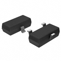


 工商网监
湘ICP备2023018690号
工商网监
湘ICP备2023018690号
