DATA SHEET
www.onsemi.com
LDO Voltage Regulator Adjustable Output, Load
Dump Protection
FIXED OUTPUT VOLTAGE
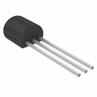
TO−92
Z SUFFIX
CASE 29−10 1
2
3
60 V, 100 mA
LM2931, NCV2931 Series
The LM2931 series consists of positive fixed and adjustable output
voltage regulators that are specifically designed to maintain proper
regulation with an extremely low input−to−output voltage differential.
These devices are capable of supplying output currents in excess of
100 mA and feature a low bias current of 0.4 mA at 10 mA output.
Designed primarily to survive in the harsh automotive environment,
these devices will protect all external load circuitry from input fault
conditions caused by reverse battery connection, two battery jump
starts, and excessive line transients during load dump. This series also
includes internal current limiting, thermal shutdown, and additionally,
is able to withstand temporary power−up with mirror−image insertion.
Due to the low dropout voltage and bias current specifications, the
LM2931 series is ideally suited for battery powered industrial and
consumer equipment where an extension of useful battery life is
desirable. The ‘C’ suffix adjustable output regulators feature an output
inhibit pin which is extremely useful in microprocessor−based systems.
Features
•
•
•
•
•
•
•
•
•
•
•
•
•
Pin 1. Output
2. Ground
3. Input
Input−to−Output Voltage Differential of < 0.6 V @ 100 mA
Output Current in Excess of 100 mA
Low Bias Current
60 V Load Dump Protection
−50 V Reverse Transient Protection
Internal Current Limiting with Thermal Shutdown
Temporary Mirror−Image Protection
Ideally Suited for Battery Powered Equipment
Economical 5−Lead TO−220 Package with Two Optional Leadforms
Available in Surface Mount SOP−8, D2PAK and DPAK Packages
High Accuracy (±2.5%) Reference (LM2931AC) Available
NCV Prefix for Automotive and Other Applications Requiring
Unique Site and Control Change Requirements; AEC−Q100
Qualified and PPAP Capable
Pb−Free Packages are Available
TO−220
T SUFFIX
CASE 221AB
1
2
3
DPAK
DT SUFFIX
CASE 369C
1
D2PAK
D2T SUFFIX
CASE 936
Pin 1. Input
2. Ground
3. Output
3
1
3
SOT−223
ST SUFFIX
CASE 318H
1
3
ADJUSTABLE OUTPUT VOLTAGE
TO−220
TH SUFFIX
CASE 314A
1
5
TO−220
1
TV SUFFIX
CASE 314B
TO−220
T SUFFIX
CASE 314D
5
1
Pin 1. Adjust
2. Output
Inhibit
3. Ground
4. Input
5. Output
5
D2PAK
D2T SUFFIX 1
CASE 936A
5
ORDERING INFORMATION
See detailed ordering and shipping information on page 12 of
this data sheet.
DEVICE MARKING INFORMATION
See general marking and heatsink information in the device
marking section on page 14 of this data sheet.
Applications
• Battery Powered Consumer Products
• Hand−held Instruments
• Camcorders and Cameras
© Semiconductor Components Industries, LLC, 2013
October, 2021 − Rev. 29
1
Publication Order Number:
LM2931/D
�LM2931, NCV2931 Series
SOIC−8
D SUFFIX
CASE 751
8
1
ADJUSTABLE
FIXED
N.C.
5
4
GND
Input
8
1
N.C.
Output
Inhibit
GND
GND
Output
Input
(Top View)
5
4
8
1
Adjust
GND
Output
(Top View)
Representative Schematic Diagram
Input
6.0
30 k
6.0 k
6.8 V
350
500
Output
Inhibit
Output
30 k
30 k
50 k
30 k *
48 k
180 k
184 k
3.94 k
Adjust
3.0 k
EPI
Bias
92.8 k *
35 k
11.5 k
Ground
*Deleted on Adjustable Regulators
This device contains 26 active transistors.
www.onsemi.com
2
10 k
5.8 V
�LM2931, NCV2931 Series
MAXIMUM RATINGS
Rating
Symbol
Value
Unit
VI
40
Vdc
Transient Input Voltage (t ≤ 100 ms)
VI(t)
60
Vpk
Transient Reverse Polarity Input Voltage
1.0% Duty Cycle, t ≤ 100 ms
−VI(t)
−50−
Vpk
−
−
−
2000
200
2000
V
V
V
PD
RqJA
RqJC
Internally Limited
178
83
W
°C/W
°C/W
PD
RqJA
RqJC
Internally Limited
65
5.0
W
°C/W
°C/W
PD
RqJA
RqJC
Internally Limited
242
21
W
°C/W
°C/W
PD
RqJA
RqJC
Internally Limited
92
6.0
W
°C/W
°C/W
PD
RqJA
RqJC
Internally Limited
160
25
W
°C/W
°C/W
PD
RqJA
RqJC
Internally Limited
70
5.0
W
°C/W
°C/W
TA
−40 to +125
°C
Input Voltage Continuous
Electrostatic Discharge Sensitivity (ESD)
Human Body Model (HBM) Class 2, JESD22 A114−C
Machine Model (MM) Class A, JESD22 A115−A
Charged Device Model (CDM), JESD22 C101−C
Power Dissipation
Case 29 (TO−92 Type)
TA = 25°C
Thermal Resistance, Junction−to−Ambient
Thermal Resistance, Junction−to−Case
Case 221A, 314A, 314B and 314D (TO−220 Type)
TA = 25°C
Thermal Resistance, Junction−to−Ambient
Thermal Resistance, Junction−to−Case
Case 318H (SOT−223)
TA = 25°C
Thermal Resistance, Junction−to−Ambient
Thermal Resistance, Junction−to−Case
Case 369A (DPAK) (Note 1)
TA = 25°C
Thermal Resistance, Junction−to−Ambient
Thermal Resistance, Junction−to−Case
Case 751 (SOP−8) (Note 2)
TA = 25°C
Thermal Resistance, Junction−to−Ambient
Thermal Resistance, Junction−to−Case
Case 936 and 936A (D2PAK) (Note 3)
TA = 25°C
Thermal Resistance, Junction−to−Ambient
Thermal Resistance, Junction−to−Case
Operating Ambient Temperature Range
Operating Die Junction Temperature
TJ
+150
°C
Storage Temperature Range
Tstg
−65 to +150
°C
Stresses exceeding those listed in the Maximum Ratings table may damage the device. If any of these limits are exceeded, device functionality
should not be assumed, damage may occur and reliability may be affected.
1. DPAK Junction−to−Ambient Thermal Resistance is for vertical mounting. Refer to Figure 25 for board mounted Thermal Resistance.
2. SOP−8 Junction−to−Ambient Thermal Resistance is for minimum recommended pad size. Refer to Figure 24 for Thermal Resistance
variation versus pad size.
3. D2PAK Junction−to−Ambient Thermal Resistance is for vertical mounting. Refer to Figure 26 for board mounted Thermal Resistance.
4. NCV rated devices are subjected to and meet the AECQ−100 quality standards.
www.onsemi.com
3
�LM2931, NCV2931 Series
ELECTRICAL CHARACTERISTICS (Vin = 14 V, IO = 10 mA, CO = 100 mF, CO(ESR) = 0.3 W, TA = 25°C [Note 5])
LM2931−5.0/NCV2931−5.0
Characteristic
Symbol
Min
Typ
Max
LM2931A−5.0/NCV2931A−5.0
Min
Typ
Max
Unit
FIXED OUTPUT
Output Voltage
VO
V
Vin = 14 V, IO = 10 mA, TA = 25°C
4.75
5.0
5.25
4.81
5.0
5.19
Vin = 6.0 V to 26 V, IO ≤ 100 mA,
TA = − 40° to +125°C
4.50
−
5.50
4.75
−
5.25
Line Regulation
Regline
mV
Vin = 9.0 V to 16 V
−
2.0
10
−
2.0
10
Vin = 6.0 V to 26 V
−
4.0
30
−
4.0
30
−
14
50
−
14
50
Load Regulation (IO = 5.0 mA to 100 mA)
Output Impedance
Regload
ZO
Bias Current
mW
−
IO = 10 mA, DIO = 1.0 mA, f = 100 Hz to
10 kHz
mV
200
−
−
200
−
IB
mA
Vin = 14 V, IO = 100 mA, TA = 25°C
−
5.8
30
−
5.8
30
Vin = 6.0 V to 26 V, IO = 10 mA, TA = − 40° to
+125°C
−
0.4
1.0
−
0.4
1.0
Output Noise Voltage (f = 10 Hz to 100 kHz)
Vn
−
700
−
−
700
−
mVrms
Long Term Stability
S
−
20
−
−
20
−
mV/kHR
RR
60
90
−
60
90
−
dB
Ripple Rejection (f = 120 Hz)
Dropout Voltage
VI−VO
V
IO = 10 mA
−
0.015
0.2
−
0.015
0.2
IO = 100 mA
−
0.16
0.6
−
0.16
0.6
Vth(OV)
26
29.5
40
26
29.5
40
V
−VO
−0.3
0
−
−0.3
0
−
V
Over−Voltage Shutdown Threshold
Output Voltage with Reverse Polarity Input
(Vin = −15 V)
5. Low duty cycle pulse techniques are used during test to maintain junction temperature as close to ambient as possible.
6. NCV devices are qualified for automotive use.
www.onsemi.com
4
�LM2931, NCV2931 Series
ELECTRICAL CHARACTERISTICS (Vin = 14 V, IO = 10 mA, CO = 100 mF, CO(ESR) = 0.3 W, TA = 25°C [Note 7])
LM2931C/NCV2931C
Characteristic
Symbol
LM2931AC/NCV2931AC
Min
Typ
Max
Min
Typ
Max
1.14
1.08
1.20
−
1.26
1.32
1.17
1.15
1.20
−
1.23
1.25
Unit
ADJUSTABLE OUTPUT
Reference Voltage (Note 8, Figure 18)
IO = 10 mA, TA = 25°C
IO ≤ 100 mA, TA = − 40 to +125°C
Vref
V
Output Voltage Range
VO range
3.0 to
24
2.7 to
29.5
−
3.0 to
24
2.7 to
29.5
−
V
Line Regulation (Vin = VO + 0.6 V to 26 V)
Regline
−
0.2
1.5
−
0.2
1.5
mV/V
Load Regulation (IO = 5.0 mA to 100 mA)
Regload
−
0.3
1.0
−
0.3
1.0
%/V
−
40
−
−
40
−
−
−
−
6.0
0.4
0.2
−
1.0
1.0
−
−
−
6.0
0.4
0.2
−
1.0
1.0
IAdj
−
0.2
−
−
0.2
−
mA
Output Noise Voltage (f = 10 Hz to 100 kHz)
Vn
−
140
−
−
140
−
mVrms/V
Long−Term Stability
S
−
0.4
−
−
0.4
−
%/kHR
RR
0.10
0.003
−
0.10
0.003
−
%/V
−
−
0.015
0.16
0.2
0.6
−
−
0.015
0.16
0.2
0.6
Output Impedance
IO = 10 mA, DIO = 1.0 mA, f = 10 Hz to 10 kHz
ZO
Bias Current
IO = 100 mA
IO = 10 mA
Output Inhibited (Vth(OI) = 2.5 V)
IB
Adjustment Pin Current
Ripple Rejection (f = 120 Hz)
mW/V
mA
Dropout Voltage
IO = 10 mA
IO = 100 mA
VI−VO
Over−Voltage Shutdown Threshold
Vth(OV)
26
29.5
40
26
29.5
40
V
−VO
−0.3
0
−
−0.3
0
−
V
−
−
2.50
3.25
2.15
−
2.26
−
1.90
1.20
−
−
−
−
2.50
3.25
2.15
−
2.26
−
1.90
1.20
−
−
−
30
50
−
30
50
Output Voltage with Reverse Polarity Input
(Vin = −15 V)
Output Inhibit Threshold Voltages
Output “On”:
TA = 25°C
TA = − 40° to +125°C
Output “Off”:
TA = 25°C
TA = − 40° to +125°C
Output Inhibit Threshold Current (Vth(OI) = 2.5 V)
V
Vth(OI)
V
Ith(OI)
7. Low duty cycle pulse techniques are used during test to maintain junction temperature as close to ambient as possible.
8. The reference voltage on the adjustable device is measured from the output to the adjust pin across R1.
www.onsemi.com
5
mA
�LM2931, NCV2931 Series
300
Vin -VO , DROPOUT VOLTAGE (mV)
Vin -VO , DROPOUT VOLTAGE (mV)
200
Vin = 14 V
DVout = 100 mV
TJ = 25°C
160
120
80
40
0
0
20
40
60
IO, OUTPUT CURRENT (mA)
80
Vin = 14 V
DVout = 100 mV
100
IO = 50 mA
IO = 10 mA
0
100
0
75
100
125
6.0
TJ = -40°C
VO , OUTPUT VOLTAGE (V)
I O , OUTPUT CURRENT (mA)
50
Figure 2. Dropout Voltage versus
Junction Temperature
350
TJ = 25°C
250
TJ = 85°C
150
Dashed lines below Vin = 5.0 V
are for Adjustable output devices only.
0
5.0
10
15
20
Vin, INPUT VOLTAGE (V)
25
Vout = 5.0 V
TA = 25°C
5.0
4.0
3.0
2.0
RL = 50 W
1.0
0
30
0
Figure 3. Peak Output Current versus Input Voltage
4.0
VO, OUTPUT VOLTAGE
(5.0 V/DIV)
3.0
2.0
Vout = 5.0 V
RL = 500 W
TA = 25°C
1.0
0
-20
-10
0
10
20
30
Vin, INPUT VOLTAGE (V)
40
50
2.0
3.0
4.0
Vin, INPUT VOLTAGE (V)
Vin , INPUT VOLTAGE
(10 V/DIV)
VCC = 15 V
VFB1 = 5.05 V
5.0
1.0
IO = 100 mA
5.0
6.0
Figure 4. Output Voltage versus Input Voltage
6.0
VO , OUTPUT VOLTAGE (V)
25
TJ, JUNCTION TEMPERATURE (°C)
Figure 1. Dropout Voltage versus Output Current
50
IO = 100 mA
200
60
Vout = 5.0 V
RL = 50 W
CO = 100 mF
t = 150 ms
TA = 25°C
0
0
Figure 5. Output Voltage versus Input Voltage
t, TIME (50 ms/DIV)
Figure 6. Load Dump Characteristics
www.onsemi.com
6
�LM2931, NCV2931 Series
8.0
10
Vout = 5.0 V
TJ = 25°C
IB , BIAS CURRENT (mA)
IB , BIAS CURRENT (mA)
12
8.0
RL = 50 W
6.0
4.0
RL = 100 W
2.0
Vin = 14 V
Vout = 5.0 V
TJ = 25°C
6.0
4.0
2.0
RL = 500 W
0
0
-20
-10
0
10
20
30
Vin, INPUT VOLTAGE (V)
40
50
60
0
40
60
80
100
IO, OUTPUT CURRENT (mA)
Figure 8. Bias Current versus Output Current
Figure 7. Bias Current versus Input Voltage
2.0
8.0
IO , OUTPUT IMPEDANCE ( Ω� )
Vin = 14 V
Vout = 5.0 V
IB , BIAS CURRENT (mA)
20
IO = 100 mA
6.0
4.0
IO = 50 mA
2.0
Vin = 14 V
Vout = 5.0 V
IO = 10 mA
DIO = 1.0 mA
CO = 100 mF
TJ = 25°C
1.6
1.2
0.8
CO(ESR) = 0.3 W
Electrolytic
0.4
CO(ESR) = 0.15 W
Tantulum
IO = 0 mA
0
-55
0
-25
0
25
50
75
TJ, JUNCTION TEMPERATURE (°C)
100
10
125
Figure 9. Bias Current versus Junction Temperature
1.0 k
10 k
100 k
f, FREQUENCY (Hz)
1.0 M
10 M
Figure 10. Output Impedance versus Frequency
95
95
RR, RIPPLE REJECTION RATIO (dB)
RR, RIPPLE REJECTION RATIO (dB)
100
85
CO(ESR) = 0.15 W
Tantulum
Vin = 14 V
Vout = 5.0 V
DVin = 100 mV
RL = 500 W
CO = 100 mF
TJ = 25°C
75
65
CO(ESR) = 0.3 W
Electrolytic
55
10
100
1.0 k
10 k
100 k
1.0 M
85
Vin = 14 V
Vout = 5.0 V
f = 120 Hz
TJ = 25°C
75
65
10 M
0
f, FREQUENCY (Hz)
Figure 11. Ripple Rejection versus Frequency
20
40
60
IO, OUTPUT CURRENT (mA)
80
100
Figure 12. Ripple Rejection versus Output Current
www.onsemi.com
7
�18.5
14
t, TIME (10 ms/DIV)
Figure 13. Line Regulation
OUTPUT CURRENT, OUTPUT VOLTAGE DEVIATION,
I out (mA)
Δ VO , (2.0 mV/DIV)
Vout = 5.0 V
RL = 500 W
CO = 100 mF
CO(ESR) = 0.3 W
TA = 25°C
V th(on/off) , OUTPUT INHIBIT‐THRESHOLDS (V)
INPUT VOLTAGE,
V in, (V)
OUTPUT VOLTAGE DEVIATION,
Δ VO , (2.0 mV/DIV)
LM2931, NCV2931 Series
Vref, REFERENCE VOLTAGE (V)
1.240
LM2931C Adjustable
IO = 10 mA
Vin = Vout + 1.0 V
TA = 25°C
1.220
1.200
1.180
1.160
0
3.0
6.0
9.0
12
15
18
21
24
Vin = 14 V
Vout = 5.0 V
Cin = 1000 mF
100
CO = 100 mF
CO(ESR) = 0.3 W
TA = 25°C
0
t, TIME (10 ms/DIV)
Figure 14. Load Regulation
2.6
LM2931C Adjustable
IO = 10 mA
Vin = Vout + 1.0 V
TA = 25°C
2.5
Output “Off"
2.4
2.3
2.2
Output “On"
2.1
2.0
0
3.0
VO, OUTPUT VOLTAGE (V)
Figure 15. Reference Voltage versus Output Voltage
6.0
9.0
12
15
18
VO, OUTPUT VOLTAGE (V)
21
24
Figure 16. Output Inhibit−Thresholds
versus Output Voltage
APPLICATIONS INFORMATION
The LM2931 series regulators are designed with many
protection features making them essentially blow−out
proof. These features include internal current limiting,
thermal shutdown, overvoltage and reverse polarity input
protection, and the capability to withstand temporary
power−up with mirror−image insertion. Typical application
circuits for the fixed and adjustable output device are shown
in Figures 17 and 18.
The input bypass capacitor Cin is recommended if the
regulator is located an appreciable distance (≥ 4″) from the
supply input filter. This will reduce the circuit’s sensitivity
to the input line impedance at high frequencies.
This regulator series is not internally compensated and
thus requires an external output capacitor for stability. The
capacitance value required is dependent upon the load
current, output voltage for the adjustable regulator, and the
type of capacitor selected. The least stable condition is
encountered at maximum load current and minimum output
voltage. Figure 22 shows that for operation in the “Stable”
region, under the conditions specified, the magnitude of the
output capacitor impedance |ZO| must not exceed 0.4 W. This
limit must be observed over the entire operating temperature
range of the regulator circuit.
With economical electrolytic capacitors, cold temperature
operation can pose a serious stability problem. As the
electrolyte freezes, around − 30°C, the capacitance will
decrease and the equivalent series resistance (ESR) will
increase drastically, causing the circuit to oscillate. Quality
electrolytic capacitors with extended temperature ranges of
−40° to +85°C and − 55° to +105°C are readily available.
Solid tantalum capacitors may be a better choice if small size
is a requirement, however, the maximum ⏐ZO⏐ limit over
temperature must be observed.
Note that in the stable region, the output noise voltage is
linearly proportional to ⏐ZO⏐. In effect, CO dictates the high
frequency roll−off point of the circuit. Operation in the area
titled “Marginally Stable” will cause the output of the
regulator to exhibit random bursts of oscillation that decay
in an under−damped fashion. Continuous oscillation occurs
when operating in the area titled “Unstable”. It is suggested
that oven testing of the entire circuit be performed with
maximum load, minimum input voltage, and minimum
ambient temperature.
www.onsemi.com
8
�LM2931, NCV2931 Series
Input
Output
Vin
Vout
51 k
Output
Inhibit
2
Cin
0.1
LM2931C
Adjustable
Output
CO
1
IAdj
Input
Cin
0.1
LM2931-5.0
Fixed
Output
IB
Output
Vout
Switch Position 1 = Output “On", 2 = Output “Off"
CO
GND
ǒ
22.5�k� w�
R 1�R 2
R 1� )� R 2
Figure 18. Adjustable Output Regulator
D45VH7
68
Ǔ
R
V out� +� V � 1� )� 2 � )� I �R 2
ref
Adj
R1
Figure 17. Fixed Output Regulator
Input
≥ 6.0 V
R2
GND
IB
Vin
R1
Adjust
RSC
Input
R
R
Output
5.0 V @ 5.0 A
LM2931-5.0
LM2931-5.0
+
+
100
+
Output
The LM2931 series can be current boosted with a PNP transistor. The
D45VH7, on a heatsink, will provide an output current of 5.0 A with an input
to output voltage differential of approximately 1.0 V. Resistor R in
conjunction with the VBE of the PNP determines when the pass transistor
begins conducting. This circuit is not short circuit proof.
Figure 20. Current Boost Regulator with
Short Circuit Projection
LM2931C
+
2.0 k
100
8.2 k
CM
#345
+
100
100
The circuit of Figure 19 can be modified to provide supply protection against
short circuits by adding the current sense resistor RSC and an additional PNP
transistor. The current sensing PNP must be capable of handling the short
circuit current of the LM2931. Safe operating area of both transistors must be
considered under worst case conditions.
Figure 19. (5.0 A) Low Differential
Voltage Regulator
Input
6.4 V to 30 V
+
100
100
33 k
6.2 V
0
fosc = 2.2 Hz
Figure 21. Constant Intensity Lamp Flasher
www.onsemi.com
9
�100
Unstable
Marginally
Stable
1.0
10 mF
22 mF
47 mF
100
mF
0.40
Unstable
0.50
ESR (Ohms)
10
0.60
Vin = 5.6 V
Vout = 5.0 V
IO = 100 mA
Vnrms 10 Hz to 10 MHz
|ZO| @ 40 kHz
TA = 25°C
0.30
Stable
0.20
0.1
Note - Optimum stability uses a 22 mF
output capacitor. Output capacitor values
below 10 mF are not recommended.
0.10
100
1.0 k
|ZO|, MAGNITUDE OF CAPACITOR IMPEDANCE (mW)
0.00
10 k
0
10
20
30
40
60
70
50
OUTPUT CURRENT (mA)
JUNCTION-TO-AIR ( °C/W)
R θ JA, THERMAL RESISTANCE
170
3.2
150
2.8
PD(max) for TA = 50°C
130
110
2.4
ÎÎÎ
ÎÎ
ÎÎÎÎÎÎ
ÎÎ
ÎÎÎÎÎÎÎÎ
2.0
Graph represents symmetrical layout
90
L
70
1.6
2.0 oz.
Copper
L
1.2
3.0 mm
0.8
50
RqJA
30
0
10
0.4
20
30
40
50
L, LENGTH OF COPPER (mm)
100
2.4
PD(max) for TA = 50°C
Free Air
Mounted
Vertically
2.0
ÎÎÎÎ
ÎÎÎÎ
ÎÎÎÎ
ÎÎÎÎ
80
Minimum
Size Pad
70
60
2.0 oz. Copper
L
1.6
L
1.2
0.8
50
0.4
RqJA
40
0
0
5.0
10
15
20
25
30
L, LENGTH OF COPPER (mm)
Figure 25. DPAK Thermal Resistance and Maximum
Power Dissipation versus P.C.B. Copper Length
www.onsemi.com
10
PD, MAXIMUM POWER DISSIPATION (W)
Figure 24. SOP−8 Thermal Resistance and Maximum
Power Dissipation versus P.C.B. Copper Length
90
80
90
100
Figure 23. Output Capacitor ESR Stability vs.
Output Load Current
PD, MAXIMUM POWER DISSIPATION (W)
Figure 22. Output Noise Voltage vs.
Output Capacitor Impedance
JUNCTION-TO-AIR ( °C/W)
0.01
10
Stable
R θ JA, THERMAL RESISTANCE
Vn , OUTPUT NOISE VOLTAGE (mVrms)
LM2931, NCV2931 Series
�3.5
PD(max) for TA = 50°C
JUNCTION-TO-AIR (° C/W)
R θ JA, THERMAL RESISTANCE
80
70
3.0
Free Air
Mounted
Vertically
60
ÎÎÎÎ
ÎÎÎÎ
ÎÎÎÎ
ÎÎÎÎ
2.0 oz. Copper
L
Minimum
Size Pad
50
2.5
2.0
L
1.5
40
RqJA
30
1.0
0
5.0
10
15
20
25
PD, MAXIMUM POWER DISSIPATION (W)
LM2931, NCV2931 Series
30
L, LENGTH OF COPPER (mm)
RqJA, THERMAL RESISTANCE,
JUNCTION−TO−AIR (°CW)
300
1.8
PD(max) for TA = 50°C
250
1.4
2.0 oz. Copper
L
ÎÎÎ
ÎÎÎ
ÎÎÎ
200
150
L
100
50
0
1.6
RqJA
0
5.0
10
15
20
25
L, LENGTH OF COPPER (mm)
1.2
1.0
0.8
0.6
0.4
0.2
0.0
30
PD, MAXIMUM POWER DISSIPATION (W)
Figure 26. 3−Pin and 5−Pin D2PAK
Thermal Resistance and Maximum Power
Dissipation versus P.C.B. Copper Length
Figure 27. SOT−223 Thermal Resistance and Maximum
Power Dissipation vs. P.C.B. Copper Length
DEFINITIONS
Maximum Power Dissipation − The maximum total
device dissipation for which the regulator will operate
within specifications.
Bias Current − That part of the input current that is not
delivered to the load.
Output Noise Voltage − The rms AC voltage at the
output, with constant load and no input ripple, measured
over a specified frequency range.
Long−Term Stability − Output voltage stability under
accelerated life test conditions with the maximum rated
voltage listed in the devices electrical characteristics and
maximum power dissipation.
Dropout Voltage − The input/output voltage differential
at which the regulator output no longer maintains regulation
against further reductions in input voltage. Measured when
the output decreases 100 mV from nominal value at 14 V
input, dropout voltage is affected by junction temperature
and load current.
Line Regulation − The change in output voltage for a
change in the input voltage. The measurement is made under
conditions of low dissipation or by using pulse techniques
such that the average chip temperature is not significantly
affected.
Load Regulation − The change in output voltage for a
change in load current at constant chip temperature.
www.onsemi.com
11
�LM2931, NCV2931 Series
ORDERING INFORMATION
Output
Voltage
Tolerance
Package
Shipping†
LM2931AD−5.0G
5.0 V
"3.8%
SOIC−8
(Pb−Free)
98 Units / Rail
LM2931AD−5.0R2G
5.0 V
"3.8%
SOIC−8
(Pb−Free)
2500 / Tape & Reel
LM2931ADT−5.0RKG
5.0 V
"3.8%
DPAK
(Pb−Free)
2500 / VacPk
LM2931AD2T−5R4G
5.0 V
"3.8%
D2PAK
(Pb−Free)
800 / VacPk Reel
LM2931AT−5.0G
5.0 V
"3.8%
TO−220
(Pb−Free)
50 Units / Rail
LM2931AZ−5.0G
5.0 V
"3.8%
TO−92
(Pb−Free)
2000 / Inner Bag
LM2931AZ−5.0RAG
5.0 V
"3.8%
TO−92
(Pb−Free)
2000 / Tape & Reel
LM2931AZ−5.0RPG
5.0 V
"3.8%
TO−92
(Pb−Free)
2000 / Ammo Pack
LM2931D−5.0R2G
5.0 V
"5.0%
SOIC−8
(Pb−Free)
2500 / Tape & Reel
LM2931D2T−5.0R4G
5.0 V
"5.0%
D2PAK
(Pb−Free)
800 / VacPk Reel
LM2931DT−5.0G
5.0 V
"5.0%
DPAK
(Pb−Free)
75 Units / Rail
LM2931T−5.0G
5.0 V
"5.0%
TO−220
(Pb−Free)
50 Units / Rail
LM2931Z−5.0G
5.0 V
"5.0%
TO−92
(Pb−Free)
2000 / Inner Bag
LM2931Z−5.0RAG
5.0 V
"5.0%
TO−92
(Pb−Free)
2000 / Tape & Reel
LM2931Z−5.0RPG
5.0 V
"5.0%
TO−92
(Pb−Free)
2000 / Ammo Pack
LM2931CDG
Adjustable
"5.0%
SOIC−8
(Pb−Free)
98 Units / Rail
LM2931CDR2G
Adjustable
"5.0%
SOIC−8
(Pb−Free)
2500 / Tape & Reel
LM2931ACDR2G
Adjustable
"2.0%
SOIC−8
(Pb−Free)
2500 / Tape & Reel
LM2931ACD2TR4G
Adjustable
"2.0%
D2PAK
(Pb−Free)
800 / VacPk Reel
NCV2931ACDR2G*
Adjustable
"2.5%
SOIC−8
(Pb−Free)
2500 / Tape & Reel
NCV2931AD−5.0R2G*
5.0 V
"3.8%
SOIC−8
(Pb−Free)
2500 / Tape & Reel
NCV2931AST−5.0T3G*
5.0 V
"3.8%
SOT−223
(Pb−Free)
4000 / Tape & Reel
NCV2931AZ−5.0G*
5.0 V
"3.8%
TO−92
(Pb−Free)
2000 / Inner Bag
Device
†For information on tape and reel specifications, including part orientation and tape sizes, please refer to our Tape and Reel Packaging Specifications Brochure, BRD8011/D.
*NCV2931: Tlow = −40°C, Thigh = +125°C. Guaranteed by design. NCV Prefix for Automotive and Other Applications Requiring Unique Site
and Control Change Requirements; AEC−Q100 Qualified and PPAP Capable.
www.onsemi.com
12
�LM2931, NCV2931 Series
ORDERING INFORMATION (continued)
Output
Voltage
Tolerance
Package
Shipping†
5.0 V
"3.8%
TO−92
(Pb−Free)
2000 / Tape & Reel
Adjustable
"5.0%
SOIC−8
(Pb−Free)
2500 / Tape & Reel
NCV2931D−5.0R2G*
5.0 V
"5.0%
SOIC−8
(Pb−Free)
2500 / Tape & Reel
NCV2931ADT5.0RKG*
5.0 V
"3.8%
DPAK
(Pb−Free)
2500 / Tape & Reel
NCV2931DT−5.0RKG*
5.0 V
"5.0%
DPAK
(Pb−Free)
2500 / Tape & Reel
NCV2931ACD2TR4G*
Adjustable
"2.5%
D2PAK
(Pb−Free)
800 / VacPk Reel
NCV2931D2T5.0R4G*
5.0 V
"5.0%
D2PAK
(Pb−Free)
800 / VacPk Reel
Device
NCV2931AZ−5.0RAG*
NCV2931CDR2G*
†For information on tape and reel specifications, including part orientation and tape sizes, please refer to our Tape and Reel Packaging Specifications Brochure, BRD8011/D.
*NCV2931: Tlow = −40°C, Thigh = +125°C. Guaranteed by design. NCV Prefix for Automotive and Other Applications Requiring Unique Site
and Control Change Requirements; AEC−Q100 Qualified and PPAP Capable.
www.onsemi.com
13
�LM2931, NCV2931 Series
MARKING DIAGRAMS
DPAK
DT SUFFIX
CASE 369A
DPAK
DT SUFFIX
CASE 369A
931A5G
ALYWW
2931G
ALYWW
*
D2PAK
D2T SUFFIX
CASE 936
D2PAK
D2T SUFFIX
CASE 936
D2PAK
D2T SUFFIX
CASE 936
LM
2931AD2T−5
AWLYWWG
LM
2931AD2T−5.0
AWLYWWG
LM
2931D2T−5
AWLYWWG
*
Heatsink surface (shown as terminal 4 in case outline drawing) is connected to Pin 2.
TO−220
T SUFFIX
CASE 221A
TO−220
T SUFFIX
CASE 221A
TO−220
T SUFFIX
CASE 314D
LM
2931AT−5
AWLYWWG
LM
2931T−5.0
AWLYWWG
LM
2931ACTV
AWLYWWG
Heatsink surface
connected to Pin 3.
Heatsink surface connected to Pin 2.
SOIC−8
D SUFFIX
CASE 751
SOIC−8
D SUFFIX
CASE 751
8
1
1
2931A
ALYW5
G
*
1
D2PAK
D2T SUFFIX
CASE 936A
LM
2931ACD2T
AWLYWWG
LM
2931CT
AWLYWWG
Heatsink surface (shown as terminal 6 in
case outline drawing) is connected to Pin 3.
SOIC−8
D SUFFIX
CASE 751
8
8
2931A
ALYW
G
SOIC−8
D SUFFIX
CASE 751
D2PAK
D2T SUFFIX
CASE 936A
8
2931C
ALYW
G
*
1
2931
ALYW5
G
SOT−223
ST SUFFIX
CASE 318H
*
ALYW
2931AG
G
1
2
3
A
WL, L
YY, Y
WW, W
G or G
= Assembly Location
= Wafer Lot
= Year
= Work Week
= Pb−Free Device
*This marking diagram also applies to NCV2931.
www.onsemi.com
14
TO−92
Z SUFFIX
CASE 029
TO−92
Z SUFFIX
CASE 029
2931A
Z−5.0
ALYW
2931Z
−5.0
ALYW
�MECHANICAL CASE OUTLINE
PACKAGE DIMENSIONS
TO−220, SINGLE GAUGE
CASE 221AB−01
ISSUE A
−T−
B
F
T
SCALE 1:1
SEATING
PLANE
C
S
DATE 16 NOV 2010
NOTES:
1. DIMENSIONING AND TOLERANCING PER ANSI Y14.5M, 1982.
2. CONTROLLING DIMENSION: INCHES.
3. DIMENSION Z DEFINES A ZONE WHERE ALL BODY AND
LEAD IRREGULARITIES ARE ALLOWED.
4. PRODUCT SHIPPED PRIOR TO 2008 HAD DIMENSIONS
S = 0.045 - 0.055 INCHES (1.143 - 1.397 MM)
4
DIM
A
B
C
D
F
G
H
J
K
L
N
Q
R
S
T
U
V
Z
A
Q
U
1 2 3
H
K
Z
L
R
V
J
G
D
N
INCHES
MIN
MAX
0.570
0.620
0.380
0.405
0.160
0.190
0.025
0.035
0.142
0.147
0.095
0.105
0.110
0.155
0.018
0.025
0.500
0.562
0.045
0.060
0.190
0.210
0.100
0.120
0.080
0.110
0.020
0.024
0.235
0.255
0.000
0.050
0.045
----0.080
MILLIMETERS
MIN
MAX
14.48
15.75
9.66
10.28
4.07
4.82
0.64
0.88
3.61
3.73
2.42
2.66
2.80
3.93
0.46
0.64
12.70
14.27
1.15
1.52
4.83
5.33
2.54
3.04
2.04
2.79
0.508
0.61
5.97
6.47
0.00
1.27
1.15
----2.04
STYLE 1:
PIN 1.
2.
3.
4.
BASE
COLLECTOR
EMITTER
COLLECTOR
STYLE 2:
PIN 1.
2.
3.
4.
BASE
EMITTER
COLLECTOR
EMITTER
STYLE 3:
PIN 1.
2.
3.
4.
CATHODE
ANODE
GATE
ANODE
STYLE 4:
PIN 1.
2.
3.
4.
MAIN TERMINAL 1
MAIN TERMINAL 2
GATE
MAIN TERMINAL 2
STYLE 5:
PIN 1.
2.
3.
4.
GATE
DRAIN
SOURCE
DRAIN
STYLE 6:
PIN 1.
2.
3.
4.
ANODE
CATHODE
ANODE
CATHODE
STYLE 7:
PIN 1.
2.
3.
4.
CATHODE
ANODE
CATHODE
ANODE
STYLE 8:
PIN 1.
2.
3.
4.
CATHODE
ANODE
EXTERNAL TRIP/DELAY
ANODE
STYLE 9:
PIN 1.
2.
3.
4.
GATE
COLLECTOR
EMITTER
COLLECTOR
STYLE 10:
PIN 1.
2.
3.
4.
GATE
SOURCE
DRAIN
SOURCE
STYLE 11:
PIN 1.
2.
3.
4.
DRAIN
SOURCE
GATE
SOURCE
DOCUMENT NUMBER:
DESCRIPTION:
98AON23085D
TO−220, SINGLE GAUGE
Electronic versions are uncontrolled except when accessed directly from the Document Repository.
Printed versions are uncontrolled except when stamped “CONTROLLED COPY” in red.
PAGE 1 OF 1
ON Semiconductor and
are trademarks of Semiconductor Components Industries, LLC dba ON Semiconductor or its subsidiaries in the United States and/or other countries.
ON Semiconductor reserves the right to make changes without further notice to any products herein. ON Semiconductor makes no warranty, representation or guarantee regarding
the suitability of its products for any particular purpose, nor does ON Semiconductor assume any liability arising out of the application or use of any product or circuit, and specifically
disclaims any and all liability, including without limitation special, consequential or incidental damages. ON Semiconductor does not convey any license under its patent rights nor the
rights of others.
© Semiconductor Components Industries, LLC, 2019
www.onsemi.com
�MECHANICAL CASE OUTLINE
PACKAGE DIMENSIONS
TO−92 (TO−226) 1 WATT
CASE 29−10
ISSUE D
SCALE 1:1
12
3
STRAIGHT LEAD
1
DATE 05 MAR 2021
2
3
BENT LEAD
STYLES AND MARKING ON PAGE 3
DOCUMENT NUMBER:
DESCRIPTION:
98AON52857E
TO−92 (TO−226) 1 WATT
Electronic versions are uncontrolled except when accessed directly from the Document Repository.
Printed versions are uncontrolled except when stamped “CONTROLLED COPY” in red.
PAGE 1 OF 3
ON Semiconductor and
are trademarks of Semiconductor Components Industries, LLC dba ON Semiconductor or its subsidiaries in the United States and/or other countries.
ON Semiconductor reserves the right to make changes without further notice to any products herein. ON Semiconductor makes no warranty, representation or guarantee regarding
the suitability of its products for any particular purpose, nor does ON Semiconductor assume any liability arising out of the application or use of any product or circuit, and specifically
disclaims any and all liability, including without limitation special, consequential or incidental damages. ON Semiconductor does not convey any license under its patent rights nor the
rights of others.
© Semiconductor Components Industries, LLC, 2019
www.onsemi.com
�MECHANICAL CASE OUTLINE
PACKAGE DIMENSIONS
TO−92 (TO−226) 1 WATT
CASE 29−10
ISSUE D
DATE 05 MAR 2021
STYLES AND MARKING ON PAGE 3
DOCUMENT NUMBER:
DESCRIPTION:
98AON52857E
TO−92 (TO−226) 1 WATT
Electronic versions are uncontrolled except when accessed directly from the Document Repository.
Printed versions are uncontrolled except when stamped “CONTROLLED COPY” in red.
PAGE 2 OF 3
ON Semiconductor and
are trademarks of Semiconductor Components Industries, LLC dba ON Semiconductor or its subsidiaries in the United States and/or other countries.
ON Semiconductor reserves the right to make changes without further notice to any products herein. ON Semiconductor makes no warranty, representation or guarantee regarding
the suitability of its products for any particular purpose, nor does ON Semiconductor assume any liability arising out of the application or use of any product or circuit, and specifically
disclaims any and all liability, including without limitation special, consequential or incidental damages. ON Semiconductor does not convey any license under its patent rights nor the
rights of others.
© Semiconductor Components Industries, LLC, 2019
www.onsemi.com
�TO−92 (TO−226) 1 WATT
CASE 29−10
ISSUE D
DATE 05 MAR 2021
STYLE 1:
PIN 1. EMITTER
2. BASE
3. COLLECTOR
STYLE 2:
PIN 1. BASE
2. EMITTER
3. COLLECTOR
STYLE 3:
PIN 1. ANODE
2. ANODE
3. CATHODE
STYLE 4:
PIN 1. CATHODE
2. CATHODE
3. ANODE
STYLE 5:
PIN 1. DRAIN
2. SOURCE
3. GATE
STYLE 6:
PIN 1. GATE
2. SOURCE & SUBSTRATE
3. DRAIN
STYLE 7:
PIN 1. SOURCE
2. DRAIN
3. GATE
STYLE 8:
PIN 1. DRAIN
2. GATE
3. SOURCE & SUBSTRATE
STYLE 9:
PIN 1. BASE 1
2. EMITTER
3. BASE 2
STYLE 10:
PIN 1. CATHODE
2. GATE
3. ANODE
STYLE 11:
PIN 1. ANODE
2. CATHODE & ANODE
3. CATHODE
STYLE 12:
PIN 1. MAIN TERMINAL 1
2. GATE
3. MAIN TERMINAL 2
STYLE 13:
PIN 1. ANODE 1
2. GATE
3. CATHODE 2
STYLE 14:
PIN 1. EMITTER
2. COLLECTOR
3. BASE
STYLE 15:
PIN 1. ANODE 1
2. CATHODE
3. ANODE 2
STYLE 16:
PIN 1. ANODE
2. GATE
3. CATHODE
STYLE 17:
PIN 1. COLLECTOR
2. BASE
3. EMITTER
STYLE 18:
PIN 1. ANODE
2. CATHODE
3. NOT CONNECTED
STYLE 19:
PIN 1. GATE
2. ANODE
3. CATHODE
STYLE 20:
PIN 1. NOT CONNECTED
2. CATHODE
3. ANODE
STYLE 21:
PIN 1. COLLECTOR
2. EMITTER
3. BASE
STYLE 22:
PIN 1. SOURCE
2. GATE
3. DRAIN
STYLE 23:
PIN 1. GATE
2. SOURCE
3. DRAIN
STYLE 24:
PIN 1. EMITTER
2. COLLECTOR/ANODE
3. CATHODE
STYLE 25:
PIN 1. MT 1
2. GATE
3. MT 2
STYLE 26:
PIN 1.
2.
3.
STYLE 27:
PIN 1. MT
2. SUBSTRATE
3. MT
STYLE 28:
PIN 1. CATHODE
2. ANODE
3. GATE
STYLE 29:
PIN 1. NOT CONNECTED
2. ANODE
3. CATHODE
STYLE 30:
PIN 1. DRAIN
2. GATE
3. SOURCE
STYLE 32:
PIN 1. BASE
2. COLLECTOR
3. EMITTER
STYLE 33:
PIN 1. RETURN
2. INPUT
3. OUTPUT
STYLE 34:
PIN 1. INPUT
2. GROUND
3. LOGIC
STYLE 35:
PIN 1. GATE
2. COLLECTOR
3. EMITTER
VCC
GROUND 2
OUTPUT
STYLE 31:
PIN 1. GATE
2. DRAIN
3. SOURCE
GENERIC
MARKING DIAGRAM*
XXXXX
XXXXX
ALYWG
G
XXXX
A
L
Y
W
G
= Specific Device Code
= Assembly Location
= Wafer Lot
= Year
= Work Week
= Pb−Free Package
(Note: Microdot may be in either location)
*This information is generic. Please refer to
device data sheet for actual part marking.
Pb−Free indicator, “G” or microdot “G”, may
or may not be present. Some products may
not follow the Generic Marking.
DOCUMENT NUMBER:
DESCRIPTION:
98AON52857E
TO−92 (TO−226) 1 WATT
Electronic versions are uncontrolled except when accessed directly from the Document Repository.
Printed versions are uncontrolled except when stamped “CONTROLLED COPY” in red.
PAGE 3 OF 3
ON Semiconductor and
are trademarks of Semiconductor Components Industries, LLC dba ON Semiconductor or its subsidiaries in the United States and/or other countries.
ON Semiconductor reserves the right to make changes without further notice to any products herein. ON Semiconductor makes no warranty, representation or guarantee regarding
the suitability of its products for any particular purpose, nor does ON Semiconductor assume any liability arising out of the application or use of any product or circuit, and specifically
disclaims any and all liability, including without limitation special, consequential or incidental damages. ON Semiconductor does not convey any license under its patent rights nor the
rights of others.
© Semiconductor Components Industries, LLC, 2019
www.onsemi.com
�MECHANICAL CASE OUTLINE
PACKAGE DIMENSIONS
TO−220 5 LEAD OFFSET
CASE 314B−05
ISSUE L
DATE 01/07/1994
SCALE 1:1
Q
OPTIONAL
CHAMFER
E
A
U
K
L
S
W
F
5X
G
5X
D
0.10 (0.254)
NOTES:
1. DIMENSIONING AND TOLERANCING PER ANSI
Y14.5M, 1982.
2. CONTROLLING DIMENSION: INCH.
3. DIMENSION D DOES NOT INCLUDE
INTERCONNECT BAR (DAMBAR) PROTRUSION.
DIMENSION D INCLUDING PROTRUSION SHALL
NOT EXCEED 0.043 (1.092) MAXIMUM.
C
B
−P−
M
T P
0.24 (0.610)
J
M
H
T
N
M
−T−
STYLE 1 THRU 4:
CANCELLED
DOCUMENT NUMBER:
DESCRIPTION:
V
98ASB42218B
TO−220 5 LEAD OFFSET
SEATING
PLANE
STYLE 5:
PIN 1.
2.
3.
4.
5.
DIM
A
B
C
D
E
F
G
H
J
K
L
N
Q
S
U
V
W
INCHES
MIN
MAX
0.572
0.613
0.390
0.415
0.170
0.180
0.025
0.038
0.048
0.055
0.850
0.935
0.067 BSC
0.166 BSC
0.015
0.025
0.900
1.100
0.320
0.365
0.320 BSC
0.140
0.153
--0.620
0.468
0.505
--0.735
0.090
0.110
MILLIMETERS
MIN
MAX
14.529 15.570
9.906 10.541
4.318
4.572
0.635
0.965
1.219
1.397
21.590 23.749
1.702 BSC
4.216 BSC
0.381
0.635
22.860 27.940
8.128
9.271
8.128 BSC
3.556
3.886
--- 15.748
11.888 12.827
--- 18.669
2.286
2.794
GATE
MIRROR
DRAIN
KELVIN
SOURCE
Electronic versions are uncontrolled except when accessed directly from the Document Repository.
Printed versions are uncontrolled except when stamped “CONTROLLED COPY” in red.
PAGE 1 OF 1
ON Semiconductor and
are trademarks of Semiconductor Components Industries, LLC dba ON Semiconductor or its subsidiaries in the United States and/or other countries.
ON Semiconductor reserves the right to make changes without further notice to any products herein. ON Semiconductor makes no warranty, representation or guarantee regarding
the suitability of its products for any particular purpose, nor does ON Semiconductor assume any liability arising out of the application or use of any product or circuit, and specifically
disclaims any and all liability, including without limitation special, consequential or incidental damages. ON Semiconductor does not convey any license under its patent rights nor the
rights of others.
© Semiconductor Components Industries, LLC, 2019
www.onsemi.com
�MECHANICAL CASE OUTLINE
PACKAGE DIMENSIONS
TO−220 5−LEAD
CASE 314D−04
ISSUE H
−T−
B
−Q−
B1
DETAIL A-A
A
U
SCALE 1:1
SEATING
PLANE
C
L
1234 5
K
D
E
DATE 29 JAN 2010
J
H
G
5 PL
0.356 (0.014)
M
T Q
M
B
B1
NOTES:
1. DIMENSIONING AND TOLERANCING PER ANSI
Y14.5M, 1982.
2. CONTROLLING DIMENSION: INCH.
3. DIMENSION D DOES NOT INCLUDE
INTERCONNECT BAR (DAMBAR) PROTRUSION.
DIMENSION D INCLUDING PROTRUSION SHALL
NOT EXCEED 10.92 (0.043) MAXIMUM.
INCHES
MIN
MAX
0.572
0.613
0.390
0.415
0.375
0.415
0.170
0.180
0.025
0.038
0.048
0.055
0.067 BSC
0.087
0.112
0.015
0.025
0.977
1.045
0.320
0.365
0.140
0.153
0.105
0.117
DIM
A
B
B1
C
D
E
G
H
J
K
L
Q
U
MILLIMETERS
MIN
MAX
14.529 15.570
9.906 10.541
9.525 10.541
4.318
4.572
0.635
0.965
1.219
1.397
1.702 BSC
2.210
2.845
0.381
0.635
24.810 26.543
8.128
9.271
3.556
3.886
2.667
2.972
STYLE 1 THRU 4:
1. OBSOLETE
GENERIC
MARKING DIAGRAM*
DETAIL A−A
XX
XXXXXXXXX
AWLYWWG
1
A
WL
Y
WW
G
= Assembly Location
= Wafer Lot
= Year
= Work Week
= Pb−Free Package
*This information is generic. Please refer to
device data sheet for actual part marking.
Pb−Free indicator, “G” or microdot “ G”,
may or may not be present.
DOCUMENT NUMBER:
DESCRIPTION:
98ASB42220B
TO−220 5−LEAD
Electronic versions are uncontrolled except when accessed directly from the Document Repository.
Printed versions are uncontrolled except when stamped “CONTROLLED COPY” in red.
PAGE 1 OF 1
ON Semiconductor and
are trademarks of Semiconductor Components Industries, LLC dba ON Semiconductor or its subsidiaries in the United States and/or other countries.
ON Semiconductor reserves the right to make changes without further notice to any products herein. ON Semiconductor makes no warranty, representation or guarantee regarding
the suitability of its products for any particular purpose, nor does ON Semiconductor assume any liability arising out of the application or use of any product or circuit, and specifically
disclaims any and all liability, including without limitation special, consequential or incidental damages. ON Semiconductor does not convey any license under its patent rights nor the
rights of others.
© Semiconductor Components Industries, LLC, 2019
www.onsemi.com
�MECHANICAL CASE OUTLINE
PACKAGE DIMENSIONS
SOT−223
CASE 318H
ISSUE B
DATE 13 MAY 2020
SCALE 2:1
GENERIC
MARKING DIAGRAM*
AYW
XXXXXG
G
1
A
= Assembly Location
Y
= Year
W
= Work Week
XXXXX = Specific Device Code
G
= Pb−Free Package
(Note: Microdot may be in either location)
*This information is generic. Please refer to
device data sheet for actual part marking.
Pb−Free indicator, “G” or microdot “G”, may
or may not be present. Some products may
not follow the Generic Marking.
DOCUMENT NUMBER:
DESCRIPTION:
98ASH70634A
SOT−223
Electronic versions are uncontrolled except when accessed directly from the Document Repository.
Printed versions are uncontrolled except when stamped “CONTROLLED COPY” in red.
PAGE 1 OF 1
ON Semiconductor and
are trademarks of Semiconductor Components Industries, LLC dba ON Semiconductor or its subsidiaries in the United States and/or other countries.
ON Semiconductor reserves the right to make changes without further notice to any products herein. ON Semiconductor makes no warranty, representation or guarantee regarding
the suitability of its products for any particular purpose, nor does ON Semiconductor assume any liability arising out of the application or use of any product or circuit, and specifically
disclaims any and all liability, including without limitation special, consequential or incidental damages. ON Semiconductor does not convey any license under its patent rights nor the
rights of others.
© Semiconductor Components Industries, LLC, 2018
www.onsemi.com
�MECHANICAL CASE OUTLINE
PACKAGE DIMENSIONS
DPAK (SINGLE GAUGE)
CASE 369C
ISSUE F
4
1 2
DATE 21 JUL 2015
3
SCALE 1:1
A
E
b3
C
A
B
c2
4
L3
Z
D
1
L4
2
3
NOTE 7
b2
e
c
SIDE VIEW
b
0.005 (0.13)
TOP VIEW
H
DETAIL A
M
BOTTOM VIEW
C
Z
H
L2
GAUGE
PLANE
C
L
L1
DETAIL A
Z
SEATING
PLANE
BOTTOM VIEW
A1
ALTERNATE
CONSTRUCTIONS
ROTATED 905 CW
STYLE 1:
PIN 1. BASE
2. COLLECTOR
3. EMITTER
4. COLLECTOR
STYLE 6:
PIN 1. MT1
2. MT2
3. GATE
4. MT2
STYLE 2:
PIN 1. GATE
2. DRAIN
3. SOURCE
4. DRAIN
STYLE 7:
PIN 1. GATE
2. COLLECTOR
3. EMITTER
4. COLLECTOR
STYLE 3:
PIN 1. ANODE
2. CATHODE
3. ANODE
4. CATHODE
STYLE 8:
PIN 1. N/C
2. CATHODE
3. ANODE
4. CATHODE
STYLE 4:
PIN 1. CATHODE
2. ANODE
3. GATE
4. ANODE
STYLE 9:
STYLE 10:
PIN 1. ANODE
PIN 1. CATHODE
2. CATHODE
2. ANODE
3. RESISTOR ADJUST
3. CATHODE
4. CATHODE
4. ANODE
SOLDERING FOOTPRINT*
6.20
0.244
2.58
0.102
5.80
0.228
INCHES
MIN
MAX
0.086 0.094
0.000 0.005
0.025 0.035
0.028 0.045
0.180 0.215
0.018 0.024
0.018 0.024
0.235 0.245
0.250 0.265
0.090 BSC
0.370 0.410
0.055 0.070
0.114 REF
0.020 BSC
0.035 0.050
−−− 0.040
0.155
−−−
MILLIMETERS
MIN
MAX
2.18
2.38
0.00
0.13
0.63
0.89
0.72
1.14
4.57
5.46
0.46
0.61
0.46
0.61
5.97
6.22
6.35
6.73
2.29 BSC
9.40 10.41
1.40
1.78
2.90 REF
0.51 BSC
0.89
1.27
−−−
1.01
3.93
−−−
GENERIC
MARKING DIAGRAM*
XXXXXXG
ALYWW
AYWW
XXX
XXXXXG
IC
Discrete
= Device Code
= Assembly Location
= Wafer Lot
= Year
= Work Week
= Pb−Free Package
*This information is generic. Please refer to
device data sheet for actual part marking.
Pb−Free indicator, “G” or microdot “G”, may
or may not be present. Some products may
not follow the Generic Marking.
6.17
0.243
SCALE 3:1
DIM
A
A1
b
b2
b3
c
c2
D
E
e
H
L
L1
L2
L3
L4
Z
XXXXXX
A
L
Y
WW
G
3.00
0.118
1.60
0.063
STYLE 5:
PIN 1. GATE
2. ANODE
3. CATHODE
4. ANODE
NOTES:
1. DIMENSIONING AND TOLERANCING PER ASME
Y14.5M, 1994.
2. CONTROLLING DIMENSION: INCHES.
3. THERMAL PAD CONTOUR OPTIONAL WITHIN DIMENSIONS b3, L3 and Z.
4. DIMENSIONS D AND E DO NOT INCLUDE MOLD
FLASH, PROTRUSIONS, OR BURRS. MOLD
FLASH, PROTRUSIONS, OR GATE BURRS SHALL
NOT EXCEED 0.006 INCHES PER SIDE.
5. DIMENSIONS D AND E ARE DETERMINED AT THE
OUTERMOST EXTREMES OF THE PLASTIC BODY.
6. DATUMS A AND B ARE DETERMINED AT DATUM
PLANE H.
7. OPTIONAL MOLD FEATURE.
mm Ǔ
ǒinches
*For additional information on our Pb−Free strategy and soldering
details, please download the ON Semiconductor Soldering and
Mounting Techniques Reference Manual, SOLDERRM/D.
DOCUMENT NUMBER:
DESCRIPTION:
98AON10527D
DPAK (SINGLE GAUGE)
Electronic versions are uncontrolled except when accessed directly from the Document Repository.
Printed versions are uncontrolled except when stamped “CONTROLLED COPY” in red.
PAGE 1 OF 1
onsemi and
are trademarks of Semiconductor Components Industries, LLC dba onsemi or its subsidiaries in the United States and/or other countries. onsemi reserves
the right to make changes without further notice to any products herein. onsemi makes no warranty, representation or guarantee regarding the suitability of its products for any particular
purpose, nor does onsemi assume any liability arising out of the application or use of any product or circuit, and specifically disclaims any and all liability, including without limitation
special, consequential or incidental damages. onsemi does not convey any license under its patent rights nor the rights of others.
© Semiconductor Components Industries, LLC, 2018
www.onsemi.com
�MECHANICAL CASE OUTLINE
PACKAGE DIMENSIONS
SOIC−8 NB
CASE 751−07
ISSUE AK
8
1
SCALE 1:1
−X−
DATE 16 FEB 2011
NOTES:
1. DIMENSIONING AND TOLERANCING PER
ANSI Y14.5M, 1982.
2. CONTROLLING DIMENSION: MILLIMETER.
3. DIMENSION A AND B DO NOT INCLUDE
MOLD PROTRUSION.
4. MAXIMUM MOLD PROTRUSION 0.15 (0.006)
PER SIDE.
5. DIMENSION D DOES NOT INCLUDE DAMBAR
PROTRUSION. ALLOWABLE DAMBAR
PROTRUSION SHALL BE 0.127 (0.005) TOTAL
IN EXCESS OF THE D DIMENSION AT
MAXIMUM MATERIAL CONDITION.
6. 751−01 THRU 751−06 ARE OBSOLETE. NEW
STANDARD IS 751−07.
A
8
5
S
B
0.25 (0.010)
M
Y
M
1
4
−Y−
K
G
C
N
X 45 _
SEATING
PLANE
−Z−
0.10 (0.004)
H
M
D
0.25 (0.010)
M
Z Y
S
X
J
S
8
8
1
1
IC
4.0
0.155
XXXXX
A
L
Y
W
G
IC
(Pb−Free)
= Specific Device Code
= Assembly Location
= Wafer Lot
= Year
= Work Week
= Pb−Free Package
XXXXXX
AYWW
1
1
Discrete
XXXXXX
AYWW
G
Discrete
(Pb−Free)
XXXXXX = Specific Device Code
A
= Assembly Location
Y
= Year
WW
= Work Week
G
= Pb−Free Package
*This information is generic. Please refer to
device data sheet for actual part marking.
Pb−Free indicator, “G” or microdot “G”, may
or may not be present. Some products may
not follow the Generic Marking.
1.270
0.050
SCALE 6:1
INCHES
MIN
MAX
0.189
0.197
0.150
0.157
0.053
0.069
0.013
0.020
0.050 BSC
0.004
0.010
0.007
0.010
0.016
0.050
0 _
8 _
0.010
0.020
0.228
0.244
8
8
XXXXX
ALYWX
G
XXXXX
ALYWX
1.52
0.060
0.6
0.024
MILLIMETERS
MIN
MAX
4.80
5.00
3.80
4.00
1.35
1.75
0.33
0.51
1.27 BSC
0.10
0.25
0.19
0.25
0.40
1.27
0_
8_
0.25
0.50
5.80
6.20
GENERIC
MARKING DIAGRAM*
SOLDERING FOOTPRINT*
7.0
0.275
DIM
A
B
C
D
G
H
J
K
M
N
S
mm Ǔ
ǒinches
*For additional information on our Pb−Free strategy and soldering
details, please download the ON Semiconductor Soldering and
Mounting Techniques Reference Manual, SOLDERRM/D.
STYLES ON PAGE 2
DOCUMENT NUMBER:
DESCRIPTION:
98ASB42564B
SOIC−8 NB
Electronic versions are uncontrolled except when accessed directly from the Document Repository.
Printed versions are uncontrolled except when stamped “CONTROLLED COPY” in red.
PAGE 1 OF 2
onsemi and
are trademarks of Semiconductor Components Industries, LLC dba onsemi or its subsidiaries in the United States and/or other countries. onsemi reserves
the right to make changes without further notice to any products herein. onsemi makes no warranty, representation or guarantee regarding the suitability of its products for any particular
purpose, nor does onsemi assume any liability arising out of the application or use of any product or circuit, and specifically disclaims any and all liability, including without limitation
special, consequential or incidental damages. onsemi does not convey any license under its patent rights nor the rights of others.
© Semiconductor Components Industries, LLC, 2019
www.onsemi.com
�SOIC−8 NB
CASE 751−07
ISSUE AK
DATE 16 FEB 2011
STYLE 1:
PIN 1. EMITTER
2. COLLECTOR
3. COLLECTOR
4. EMITTER
5. EMITTER
6. BASE
7. BASE
8. EMITTER
STYLE 2:
PIN 1. COLLECTOR, DIE, #1
2. COLLECTOR, #1
3. COLLECTOR, #2
4. COLLECTOR, #2
5. BASE, #2
6. EMITTER, #2
7. BASE, #1
8. EMITTER, #1
STYLE 3:
PIN 1. DRAIN, DIE #1
2. DRAIN, #1
3. DRAIN, #2
4. DRAIN, #2
5. GATE, #2
6. SOURCE, #2
7. GATE, #1
8. SOURCE, #1
STYLE 4:
PIN 1. ANODE
2. ANODE
3. ANODE
4. ANODE
5. ANODE
6. ANODE
7. ANODE
8. COMMON CATHODE
STYLE 5:
PIN 1. DRAIN
2. DRAIN
3. DRAIN
4. DRAIN
5. GATE
6. GATE
7. SOURCE
8. SOURCE
STYLE 6:
PIN 1. SOURCE
2. DRAIN
3. DRAIN
4. SOURCE
5. SOURCE
6. GATE
7. GATE
8. SOURCE
STYLE 7:
PIN 1. INPUT
2. EXTERNAL BYPASS
3. THIRD STAGE SOURCE
4. GROUND
5. DRAIN
6. GATE 3
7. SECOND STAGE Vd
8. FIRST STAGE Vd
STYLE 8:
PIN 1. COLLECTOR, DIE #1
2. BASE, #1
3. BASE, #2
4. COLLECTOR, #2
5. COLLECTOR, #2
6. EMITTER, #2
7. EMITTER, #1
8. COLLECTOR, #1
STYLE 9:
PIN 1. EMITTER, COMMON
2. COLLECTOR, DIE #1
3. COLLECTOR, DIE #2
4. EMITTER, COMMON
5. EMITTER, COMMON
6. BASE, DIE #2
7. BASE, DIE #1
8. EMITTER, COMMON
STYLE 10:
PIN 1. GROUND
2. BIAS 1
3. OUTPUT
4. GROUND
5. GROUND
6. BIAS 2
7. INPUT
8. GROUND
STYLE 11:
PIN 1. SOURCE 1
2. GATE 1
3. SOURCE 2
4. GATE 2
5. DRAIN 2
6. DRAIN 2
7. DRAIN 1
8. DRAIN 1
STYLE 12:
PIN 1. SOURCE
2. SOURCE
3. SOURCE
4. GATE
5. DRAIN
6. DRAIN
7. DRAIN
8. DRAIN
STYLE 13:
PIN 1. N.C.
2. SOURCE
3. SOURCE
4. GATE
5. DRAIN
6. DRAIN
7. DRAIN
8. DRAIN
STYLE 14:
PIN 1. N−SOURCE
2. N−GATE
3. P−SOURCE
4. P−GATE
5. P−DRAIN
6. P−DRAIN
7. N−DRAIN
8. N−DRAIN
STYLE 15:
PIN 1. ANODE 1
2. ANODE 1
3. ANODE 1
4. ANODE 1
5. CATHODE, COMMON
6. CATHODE, COMMON
7. CATHODE, COMMON
8. CATHODE, COMMON
STYLE 16:
PIN 1. EMITTER, DIE #1
2. BASE, DIE #1
3. EMITTER, DIE #2
4. BASE, DIE #2
5. COLLECTOR, DIE #2
6. COLLECTOR, DIE #2
7. COLLECTOR, DIE #1
8. COLLECTOR, DIE #1
STYLE 17:
PIN 1. VCC
2. V2OUT
3. V1OUT
4. TXE
5. RXE
6. VEE
7. GND
8. ACC
STYLE 18:
PIN 1. ANODE
2. ANODE
3. SOURCE
4. GATE
5. DRAIN
6. DRAIN
7. CATHODE
8. CATHODE
STYLE 19:
PIN 1. SOURCE 1
2. GATE 1
3. SOURCE 2
4. GATE 2
5. DRAIN 2
6. MIRROR 2
7. DRAIN 1
8. MIRROR 1
STYLE 20:
PIN 1. SOURCE (N)
2. GATE (N)
3. SOURCE (P)
4. GATE (P)
5. DRAIN
6. DRAIN
7. DRAIN
8. DRAIN
STYLE 21:
PIN 1. CATHODE 1
2. CATHODE 2
3. CATHODE 3
4. CATHODE 4
5. CATHODE 5
6. COMMON ANODE
7. COMMON ANODE
8. CATHODE 6
STYLE 22:
PIN 1. I/O LINE 1
2. COMMON CATHODE/VCC
3. COMMON CATHODE/VCC
4. I/O LINE 3
5. COMMON ANODE/GND
6. I/O LINE 4
7. I/O LINE 5
8. COMMON ANODE/GND
STYLE 23:
PIN 1. LINE 1 IN
2. COMMON ANODE/GND
3. COMMON ANODE/GND
4. LINE 2 IN
5. LINE 2 OUT
6. COMMON ANODE/GND
7. COMMON ANODE/GND
8. LINE 1 OUT
STYLE 24:
PIN 1. BASE
2. EMITTER
3. COLLECTOR/ANODE
4. COLLECTOR/ANODE
5. CATHODE
6. CATHODE
7. COLLECTOR/ANODE
8. COLLECTOR/ANODE
STYLE 25:
PIN 1. VIN
2. N/C
3. REXT
4. GND
5. IOUT
6. IOUT
7. IOUT
8. IOUT
STYLE 26:
PIN 1. GND
2. dv/dt
3. ENABLE
4. ILIMIT
5. SOURCE
6. SOURCE
7. SOURCE
8. VCC
STYLE 29:
PIN 1. BASE, DIE #1
2. EMITTER, #1
3. BASE, #2
4. EMITTER, #2
5. COLLECTOR, #2
6. COLLECTOR, #2
7. COLLECTOR, #1
8. COLLECTOR, #1
STYLE 30:
PIN 1. DRAIN 1
2. DRAIN 1
3. GATE 2
4. SOURCE 2
5. SOURCE 1/DRAIN 2
6. SOURCE 1/DRAIN 2
7. SOURCE 1/DRAIN 2
8. GATE 1
DOCUMENT NUMBER:
DESCRIPTION:
98ASB42564B
SOIC−8 NB
STYLE 27:
PIN 1. ILIMIT
2. OVLO
3. UVLO
4. INPUT+
5. SOURCE
6. SOURCE
7. SOURCE
8. DRAIN
STYLE 28:
PIN 1. SW_TO_GND
2. DASIC_OFF
3. DASIC_SW_DET
4. GND
5. V_MON
6. VBULK
7. VBULK
8. VIN
Electronic versions are uncontrolled except when accessed directly from the Document Repository.
Printed versions are uncontrolled except when stamped “CONTROLLED COPY” in red.
PAGE 2 OF 2
onsemi and
are trademarks of Semiconductor Components Industries, LLC dba onsemi or its subsidiaries in the United States and/or other countries. onsemi reserves
the right to make changes without further notice to any products herein. onsemi makes no warranty, representation or guarantee regarding the suitability of its products for any particular
purpose, nor does onsemi assume any liability arising out of the application or use of any product or circuit, and specifically disclaims any and all liability, including without limitation
special, consequential or incidental damages. onsemi does not convey any license under its patent rights nor the rights of others.
© Semiconductor Components Industries, LLC, 2019
www.onsemi.com
�MECHANICAL CASE OUTLINE
PACKAGE DIMENSIONS
D2PAK
CASE 936−03
ISSUE E
DATE 29 SEP 2015
SCALE 1:1
T
C
A
K
B
J
C
ES
OPTIONAL
CHAMFER
DETAIL C
DETAIL C
3
F
G
SIDE VIEW
2X
TOP VIEW
D
0.010 (0.254)
N
DUAL GAUGE
CONSTRUCTION
P
BOTTOM VIEW
SIDE VIEW
SINGLE GAUGE
CONSTRUCTION
T
M
M
R
T
V
H
2
U
ED
OPTIONAL
CHAMFER
S
1
TERMINAL 4
T
SEATING
PLANE
L
BOTTOM VIEW
DETAIL C
OPTIONAL CONSTRUCTIONS
NOTES:
1. DIMENSIONING AND TOLERANCING PER ANSI
Y14.5M, 1982.
2. CONTROLLING DIMENSION: INCHES.
3. TAB CONTOUR OPTIONAL WITHIN DIMENSIONS
A AND K.
4. DIMENSIONS U AND V ESTABLISH A MINIMUM
MOUNTING SURFACE FOR TERMINAL 4.
5. DIMENSIONS A AND B DO NOT INCLUDE MOLD
FLASH OR GATE PROTRUSIONS. MOLD FLASH
AND GATE PROTRUSIONS NOT TO EXCEED
0.025 (0.635) MAXIMUM.
6. SINGLE GAUGE DESIGN WILL BE SHIPPED AF
TER FPCN EXPIRATION IN OCTOBER 2011.
DIM
A
B
C
D
ED
ES
F
G
H
J
K
L
M
N
P
R
S
U
V
INCHES
MIN
MAX
0.386
0.403
0.356
0.368
0.170
0.180
0.026
0.036
0.045
0.055
0.018
0.026
0.051 REF
0.100 BSC
0.539
0.579
0.125 MAX
0.050 REF
0.000
0.010
0.088
0.102
0.018
0.026
0.058
0.078
0_
8_
0.116 REF
0.200 MIN
0.250 MIN
MILLIMETERS
MIN
MAX
9.804 10.236
9.042
9.347
4.318
4.572
0.660
0.914
1.143
1.397
0.457
0.660
1.295 REF
2.540 BSC
13.691 14.707
3.175 MAX
1.270 REF
0.000
0.254
2.235
2.591
0.457
0.660
1.473
1.981
0_
8_
2.946 REF
5.080 MIN
6.350 MIN
GENERIC
MARKING DIAGRAM*
SOLDERING FOOTPRINT*
10.490
XXXXXXG
ALYWW
8.380
16.155
XXXXXX = Specific Device Code
A
= Assembly Location
L
= Wafer Lot
Y
= Year
WW
= Work Week
G
= Pb−Free Package
2X
3.504
2X
1.016
5.080
PITCH
DIMENSIONS: MILLIMETERS
*For additional information on our Pb−Free strategy and soldering
details, please download the ON Semiconductor Soldering and
Mounting Techniques Reference Manual, SOLDERRM/D.
DOCUMENT NUMBER:
DESCRIPTION:
98ASH01005A
D2PAK
*This information is generic. Please refer to
device data sheet for actual part marking.
Pb−Free indicator, “G” or microdot “ G”,
may or may not be present.
Electronic versions are uncontrolled except when accessed directly from the Document Repository.
Printed versions are uncontrolled except when stamped “CONTROLLED COPY” in red.
PAGE 1 OF 1
ON Semiconductor and
are trademarks of Semiconductor Components Industries, LLC dba ON Semiconductor or its subsidiaries in the United States and/or other countries.
ON Semiconductor reserves the right to make changes without further notice to any products herein. ON Semiconductor makes no warranty, representation or guarantee regarding
the suitability of its products for any particular purpose, nor does ON Semiconductor assume any liability arising out of the application or use of any product or circuit, and specifically
disclaims any and all liability, including without limitation special, consequential or incidental damages. ON Semiconductor does not convey any license under its patent rights nor the
rights of others.
© Semiconductor Components Industries, LLC, 2019
www.onsemi.com
�MECHANICAL CASE OUTLINE
PACKAGE DIMENSIONS
D2PAK 5−LEAD
CASE 936A−02
ISSUE E
DATE 28 JUL 2021
SCALE 1:1
GENERIC
MARKING DIAGRAM*
xx
xxxxxxxxx
AWLYWWG
xxxxxx
A
WL
Y
WW
G
= Device Code
= Assembly Location
= Wafer Lot
= Year
= Work Week
= Pb−Free Package
*This information is generic. Please refer to
device data sheet for actual part marking.
Pb−Free indicator, “G” or microdot “G”, may
or may not be present. Some products may
not follow the Generic Marking.
DOCUMENT NUMBER:
DESCRIPTION:
98ASH01006A
D2PAK 5−LEAD
Electronic versions are uncontrolled except when accessed directly from the Document Repository.
Printed versions are uncontrolled except when stamped “CONTROLLED COPY” in red.
PAGE 1 OF 1
ON Semiconductor and
are trademarks of Semiconductor Components Industries, LLC dba ON Semiconductor or its subsidiaries in the United States and/or other countries.
ON Semiconductor reserves the right to make changes without further notice to any products herein. ON Semiconductor makes no warranty, representation or guarantee regarding
the suitability of its products for any particular purpose, nor does ON Semiconductor assume any liability arising out of the application or use of any product or circuit, and specifically
disclaims any and all liability, including without limitation special, consequential or incidental damages. ON Semiconductor does not convey any license under its patent rights nor the
rights of others.
© Semiconductor Components Industries, LLC, 2019
www.onsemi.com
�onsemi,
, and other names, marks, and brands are registered and/or common law trademarks of Semiconductor Components Industries, LLC dba “onsemi” or its affiliates
and/or subsidiaries in the United States and/or other countries. onsemi owns the rights to a number of patents, trademarks, copyrights, trade secrets, and other intellectual property.
A listing of onsemi’s product/patent coverage may be accessed at www.onsemi.com/site/pdf/Patent−Marking.pdf. onsemi reserves the right to make changes at any time to any
products or information herein, without notice. The information herein is provided “as−is” and onsemi makes no warranty, representation or guarantee regarding the accuracy of the
information, product features, availability, functionality, or suitability of its products for any particular purpose, nor does onsemi assume any liability arising out of the application or use
of any product or circuit, and specifically disclaims any and all liability, including without limitation special, consequential or incidental damages. Buyer is responsible for its products
and applications using onsemi products, including compliance with all laws, regulations and safety requirements or standards, regardless of any support or applications information
provided by onsemi. “Typical” parameters which may be provided in onsemi data sheets and/or specifications can and do vary in different applications and actual performance may
vary over time. All operating parameters, including “Typicals” must be validated for each customer application by customer’s technical experts. onsemi does not convey any license
under any of its intellectual property rights nor the rights of others. onsemi products are not designed, intended, or authorized for use as a critical component in life support systems
or any FDA Class 3 medical devices or medical devices with a same or similar classification in a foreign jurisdiction or any devices intended for implantation in the human body. Should
Buyer purchase or use onsemi products for any such unintended or unauthorized application, Buyer shall indemnify and hold onsemi and its officers, employees, subsidiaries, affiliates,
and distributors harmless against all claims, costs, damages, and expenses, and reasonable attorney fees arising out of, directly or indirectly, any claim of personal injury or death
associated with such unintended or unauthorized use, even if such claim alleges that onsemi was negligent regarding the design or manufacture of the part. onsemi is an Equal
Opportunity/Affirmative Action Employer. This literature is subject to all applicable copyright laws and is not for resale in any manner.
PUBLICATION ORDERING INFORMATION
LITERATURE FULFILLMENT:
Email Requests to: orderlit@onsemi.com
onsemi Website: www.onsemi.com
◊
TECHNICAL SUPPORT
North American Technical Support:
Voice Mail: 1 800−282−9855 Toll Free USA/Canada
Phone: 011 421 33 790 2910
Europe, Middle East and Africa Technical Support:
Phone: 00421 33 790 2910
For additional information, please contact your local Sales Representative
�


 工商网监
湘ICP备2023018690号
工商网监
湘ICP备2023018690号
