MGSF1N02L, MVGSF1N02L
Power MOSFET
750 mAmps, 20 Volts
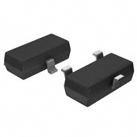
N−Channel SOT−23
These miniature surface mount MOSFETs low RDS(on) assure
minimal power loss and conserve energy, making these devices ideal
for use in space sensitive power management circuitry. Typical
applications are dc−dc converters and power management in portable
and battery−powered products such as computers, printers, PCMCIA
cards, cellular and cordless telephones.
www.onsemi.com
750 mAMPS, 20 VOLTS
RDS(on) = 90 mW
N−Channel
3
Features
• Low RDS(on) Provides Higher Efficiency and Extends Battery Life
• Miniature SOT−23 Surface Mount Package Saves Board Space
• MVGSF Prefix for Automotive and Other Applications Requiring
•
Unique Site and Control Change Requirements; AEC−Q101
Qualified and PPAP Capable*
These Devices are Pb−Free and are RoHS Compliant
1
2
MAXIMUM RATINGS (TJ = 25°C unless otherwise noted)
Symbol
Value
Unit
Drain−to−Source Voltage
VDSS
20
Vdc
Gate−to−Source Voltage − Continuous
VGS
± 20
Vdc
Rating
Drain Current
− Continuous @ TA = 25°C
− Pulsed Drain Current (tp ≤ 10 ms)
3
Drain
1
ID
IDM
750
2000
mA
PD
400
mW
Operating and Storage Temperature Range
TJ, Tstg
− 55 to 150
°C
Thermal Resistance, Junction−to−Ambient
RqJA
300
°C/W
Maximum Lead Temperature for Soldering
Purposes, 1/8″ from case for 10 seconds
TL
260
°C
Total Power Dissipation @ TA = 25°C
MARKING DIAGRAM/
PIN ASSIGNMENT
Stresses exceeding those listed in the Maximum Ratings table may damage the
device. If any of these limits are exceeded, device functionality should not be
assumed, damage may occur and reliability may be affected.
SOT−23
CASE 318
STYLE 21
N2 M G
G
1
Gate
2
Source
N2
= Device Code
M
= Date Code*
G
= Pb−Free Package
(Note: Microdot may be in either location)
*Date Code orientation and overbar may vary
depending upon manufacturing location.
ORDERING INFORMATION
Package
Shipping†
MGSF1N02LT1G
SOT−23
(Pb−Free)
3000 / Tape &
Reel
MVGSF1N02LT1G*
SOT−23
(Pb−Free)
3000 / Tape &
Reel
Device
†For information on tape and reel specifications,
including part orientation and tape sizes, please
refer to our Tape and Reel Packaging Specifications
Brochure, BRD8011/D.
© Semiconductor Components Industries, LLC, 1996
October, 2016 − Rev. 7
1
Publication Order Number:
MGSF1N02LT1/D
�MGSF1N02L, MVGSF1N02L
ELECTRICAL CHARACTERISTICS (TA = 25°C unless otherwise noted)
Characteristic
Symbol
Min
Typ
Max
Unit
V(BR)DSS
20
−
−
Vdc
−
−
−
−
1.0
10
OFF CHARACTERISTICS
Drain−to−Source Breakdown Voltage
(VGS = 0 Vdc, ID = 10 mAdc)
Zero Gate Voltage Drain Current
(VDS = 20 Vdc, VGS = 0 Vdc)
(VDS = 20 Vdc, VGS = 0 Vdc, TJ = 125°C)
IDSS
Gate−Body Leakage Current (VGS = ± 20 Vdc, VDS = 0 Vdc)
IGSS
−
−
±100
nAdc
Gate Threshold Voltage
(VDS = VGS, ID = 250 mAdc)
VGS(th)
1.0
1.7
2.4
Vdc
Static Drain−to−Source On−Resistance
(VGS = 10 Vdc, ID = 1.2 Adc)
(VGS = 4.5 Vdc, ID = 1.0 Adc)
rDS(on)
−
−
0.075
0.115
0.090
0.130
mAdc
ON CHARACTERISTICS (Note 1)
W
DYNAMIC CHARACTERISTICS
Input Capacitance
(VDS = 5.0 Vdc)
Ciss
−
125
−
pF
Output Capacitance
(VDS = 5.0 Vdc)
Coss
−
120
−
Transfer Capacitance
(VDG = 5.0 Vdc)
Crss
−
45
−
td(on)
−
2.5
−
tr
−
1.0
−
td(off)
−
16
−
tf
−
8.0
−
QT
−
6000
−
pC
IS
−
−
0.6
A
Pulsed Current
ISM
−
−
0.75
−
Forward Voltage (Note 2)
VSD
−
0.8
−
V
SWITCHING CHARACTERISTICS (Note 2)
Turn−On Delay Time
Rise Time
(VDD = 15 Vdc, ID = 1.0 Adc,
RL = 50 W)
Turn−Off Delay Time
Fall Time
Gate Charge (See Figure 6)
ns
SOURCE−DRAIN DIODE CHARACTERISTICS
Continuous Current
Product parametric performance is indicated in the Electrical Characteristics for the listed test conditions, unless otherwise noted. Product
performance may not be indicated by the Electrical Characteristics if operated under different conditions.
1. Pulse Test: Pulse Width ≤ 300 ms, Duty Cycle ≤ 2%.
2. Switching characteristics are independent of operating junction temperature.
TYPICAL ELECTRICAL CHARACTERISTICS
3
2.5
4V
I D , DRAIN CURRENT (AMPS)
I D , DRAIN CURRENT (AMPS)
VDS = 10 V
2
- 55°C
1.5
TJ = 150°C
1
0.5
1
1.5
2
2.5
3.25 V
3.5 V
2
VGS = 3.0 V
1.5
2.75 V
1
2.5 V
0.5
25°C
0
2.5
2.25 V
3
0
3.5
VGS, GATE-TO-SOURCE VOLTAGE (VOLTS)
0
2
4
6
8
3
5
7
VDS, DRAIN-TO-SOURCE VOLTAGE (VOLTS)
Figure 1. Transfer Characteristics
Figure 2. On−Region Characteristics
www.onsemi.com
2
1
9
10
�MGSF1N02L, MVGSF1N02L
R DS(on) , DRAIN-TO-SOURCE RESISTANCE (OHMS)
R DS(on) , DRAIN-TO-SOURCE RESISTANCE (OHMS)
TYPICAL ELECTRICAL CHARACTERISTICS
0.2
150°C
0.18
0.16
VGS = 4.5 V
0.14
25°C
0.12
-55°C
0.1
0.08
0.06
0.04
0
0.1
0.3
0.2
0.4
0.5
0.6
0.7
0.8
0.9
1
0.14
0.13
150°C
0.12
VGS = 10 V
0.11
0.1
0.09
25°C
0.08
0.07
-55°C
0.06
0.05
0.04
0
0.2
0.4
0.6
ID, DRAIN CURRENT (AMPS)
VGS, GATE-TO-SOURCE VOLTAGE (VOLTS)
RDS(on) , DRAIN-TO-SOURCE RESISTANCE
(NORMALIZED)
1.6
VGS = 10 V
ID = 2 A
1.4
1.3
VGS = 4.5 V
ID = 1 A
1.2
1.1
1
0.9
0.8
0.7
1.2
1.6
1.4
1.8
2
10
VDS = 16 V
TJ = 25°C
8
6
4
ID = 2.0 A
2
0
0.6
-�55
-5
45
95
145
0
2000
1000
TJ, JUNCTION TEMPERATURE (°C)
3000
4000
5000
6000
QT, TOTAL GATE CHARGE (pC)
Figure 6. Gate Charge
Figure 5. On−Resistance Variation with Temperature
1
1000
TJ = 150°C
0.1
25°C
VGS = 0 V
f = 1 MHz
TJ = 25°C
-55°C
C, CAPACITANCE (pF)
I D , DIODE CURRENT (AMPS)
1
Figure 4. On−Resistance versus Drain Current
Figure 3. On−Resistance versus Drain Current
1.5
0.8
ID, DRAIN CURRENT (AMPS)
0.01
Ciss
100
Coss
Crss
0.001
0
0.2
0.4
0.6
10
1
0.8
0
5
10
15
VDS, DRAIN-TO-SOURCE VOLTAGE (Volts)
VSD, DIODE FORWARD VOLTAGE (VOLTS)
Figure 7. Body Diode Forward Voltage
Figure 8. Capacitance
www.onsemi.com
3
20
�MGSF1N02L, MVGSF1N02L
PACKAGE DIMENSIONS
SOT−23 (TO−236)
CASE 318−08
ISSUE AR
D
0.25
3
E
1
2
T
HE
NOTES:
1. DIMENSIONING AND TOLERANCING PER ASME Y14.5M, 1994.
2. CONTROLLING DIMENSION: MILLIMETERS.
3. MAXIMUM LEAD THICKNESS INCLUDES LEAD FINISH.
MINIMUM LEAD THICKNESS IS THE MINIMUM THICKNESS OF
THE BASE MATERIAL.
4. DIMENSIONS D AND E DO NOT INCLUDE MOLD FLASH,
PROTRUSIONS, OR GATE BURRS.
DIM
A
A1
b
c
D
E
e
L
L1
HE
T
L
3X b
L1
VIEW C
e
TOP VIEW
A
A1
SIDE VIEW
c
SEE VIEW C
MIN
0.89
0.01
0.37
0.08
2.80
1.20
1.78
0.30
0.35
2.10
0_
MILLIMETERS
NOM
MAX
1.00
1.11
0.06
0.10
0.44
0.50
0.14
0.20
2.90
3.04
1.30
1.40
1.90
2.04
0.43
0.55
0.54
0.69
2.40
2.64
−−−
10 _
MIN
0.035
0.000
0.015
0.003
0.110
0.047
0.070
0.012
0.014
0.083
0_
INCHES
NOM
MAX
0.039
0.044
0.002
0.004
0.017
0.020
0.006
0.008
0.114
0.120
0.051
0.055
0.075
0.080
0.017
0.022
0.021
0.027
0.094
0.104
−−−
10 _
STYLE 21:
PIN 1. GATE
2. SOURCE
3. DRAIN
END VIEW
RECOMMENDED
SOLDERING FOOTPRINT*
3X
2.90
3X
0.90
0.95
PITCH
0.80
DIMENSIONS: MILLIMETERS
*For additional information on our Pb−Free strategy and soldering
details, please download the ON Semiconductor Soldering and
Mounting Techniques Reference Manual, SOLDERRM/D.
ON Semiconductor and
are trademarks of Semiconductor Components Industries, LLC dba ON Semiconductor or its subsidiaries in the United States and/or other countries.
ON Semiconductor owns the rights to a number of patents, trademarks, copyrights, trade secrets, and other intellectual property. A listing of ON Semiconductor’s product/patent
coverage may be accessed at www.onsemi.com/site/pdf/Patent−Marking.pdf. ON Semiconductor reserves the right to make changes without further notice to any products herein.
ON Semiconductor makes no warranty, representation or guarantee regarding the suitability of its products for any particular purpose, nor does ON Semiconductor assume any liability
arising out of the application or use of any product or circuit, and specifically disclaims any and all liability, including without limitation special, consequential or incidental damages.
Buyer is responsible for its products and applications using ON Semiconductor products, including compliance with all laws, regulations and safety requirements or standards,
regardless of any support or applications information provided by ON Semiconductor. “Typical” parameters which may be provided in ON Semiconductor data sheets and/or
specifications can and do vary in different applications and actual performance may vary over time. All operating parameters, including “Typicals” must be validated for each customer
application by customer’s technical experts. ON Semiconductor does not convey any license under its patent rights nor the rights of others. ON Semiconductor products are not
designed, intended, or authorized for use as a critical component in life support systems or any FDA Class 3 medical devices or medical devices with a same or similar classification
in a foreign jurisdiction or any devices intended for implantation in the human body. Should Buyer purchase or use ON Semiconductor products for any such unintended or unauthorized
application, Buyer shall indemnify and hold ON Semiconductor and its officers, employees, subsidiaries, affiliates, and distributors harmless against all claims, costs, damages, and
expenses, and reasonable attorney fees arising out of, directly or indirectly, any claim of personal injury or death associated with such unintended or unauthorized use, even if such
claim alleges that ON Semiconductor was negligent regarding the design or manufacture of the part. ON Semiconductor is an Equal Opportunity/Affirmative Action Employer. This
literature is subject to all applicable copyright laws and is not for resale in any manner.
PUBLICATION ORDERING INFORMATION
LITERATURE FULFILLMENT:
Literature Distribution Center for ON Semiconductor
19521 E. 32nd Pkwy, Aurora, Colorado 80011 USA
Phone: 303−675−2175 or 800−344−3860 Toll Free USA/Canada
Fax: 303−675−2176 or 800−344−3867 Toll Free USA/Canada
Email: orderlit@onsemi.com
◊
N. American Technical Support: 800−282−9855 Toll Free
USA/Canada
Europe, Middle East and Africa Technical Support:
Phone: 421 33 790 2910
Japan Customer Focus Center
Phone: 81−3−5817−1050
www.onsemi.com
4
ON Semiconductor Website: www.onsemi.com
Order Literature: http://www.onsemi.com/orderlit
For additional information, please contact your local
Sales Representative
MGSF1N02LT1/D
�


 工商网监
湘ICP备2023018690号
工商网监
湘ICP备2023018690号
