74VHC541 Octal Buffer Line Driver with TRI-STATE Outputs
November 1995
74VHC541 Octal Buffer Line Driver with TRI-STATE Outputs
General Description
The VHC541 is an advanced high-speed CMOS device fabricated with silicon gate CMOS technology It achieves the high-speed operation similar to equivalent Bipolar Schottky TTL while maintaining the CMOS low power dissipation The VHC541 is an octal buffer line driver designed to be employed as memory and address drivers clock drivers and bus oriented transmitter receivers This device is similar in function to the VHC244 while providing flow-through architecture (inputs on opposite side from outputs) This pinout arrangement makes this device especially useful as an output port for microprocessors allowing ease of layout and greater PC board density An input protection circuit insures that 0V to 7V can be applied to the input pins without regard to the supply voltage This device can be used to interface 5V to 3V systems and two supply systems such as battery backup This circuit prevents device destruction due to mismatched supply and input voltages
Features
Y Y Y
Y Y Y
Low power dissipation ICC e 4 mA (max) at TA e 25 C High noise immunity VNIH e VNIL e 28% VCC (min) All inputs are equipped with a power down protection function Balanced propagation delays tPLH j tPHL Low noise VOLP e 0 9V (typ) Pin and function compatible with 74HC541
Commercial 74VHC541M 74VHC541SJ 74VHC541MTC 74VHC541N
Package Number M20B M20D MTC20 N20A
Package Description 20-Lead Molded JEDEC SOIC 20-Lead Molded EIAJ SOIC 20-Lead Molded JEDEC Type 1 TSSOP 20-Lead Molded DIP
Note Surface mount packages are also available on Tape and Reel Specify by appending the suffix letter ‘‘X’’ to the ordering code
Logic Symbol
IEEE IEC
Connection Diagram
Pin Assignment for DIP TSSOP and SOIC
Truth Table
Inputs OE1 L H X L OE2 L X H L I H X X L Outputs H Z Z L
H e HIGH Voltage Level L e LOW Voltage Level X e Immaterial Z e High Impedance
TL F 11639 – 2
TL F 11639–1
TRI-STATE is a registered trademark of National Semiconductor Corporation
C1995 National Semiconductor Corporation
TL F 11639
RRD-B30M125 Printed in U S A
�Absolute Maximum Ratings (Note 1)
Supply Voltage (VCC) DC Input Voltage (VIN) DC Output Voltage (VOUT) Input Diode Current (IIK) Output Diode Current (IOK) DC Output Current (IOUT) DC VCC GND Current (ICC) Storage Temperature (TSTG) Lead Temperature (TL) (Soldering 10 seconds)
b 0 5V to a 7 0V b 0 5V to a 7 0V b 0 5V to VCC a 0 5V b 20 mA
g 20 mA g 25 mA g 75 mA
Note 1 Absolute Maximum Ratings are values beyond which the device may be damaged or have its useful life impaired The databook specifications should be met without exception to ensure that the system design is reliable over its power supply temperature and output input loading variables National does not recommend operation outside databook specifications
b 65 C to a 150 C
Recommended Operating Conditions
Supply Voltage (VCC) Input Voltage (VIN) Output Voltage (VOUT) Operating Temperature (TOPR) Input Rise and Fall Time (tr tf) VCC e 3 3V g 0 3V VCC e 5 0V g 0 5V 2 0V to a 5 5V 0V to a 5 5V 0V to VCC
b 40 C to a 85 C
260 C
0 E 100 ns V 0 E 20 ns V
DC Characteristics for ’VHC Family Devices
74VHC Symbol Parameter VCC (V) Min VIH VIL VOH High Level Input Voltage Low Level Input Voltage High Level Output Voltage 20 3 0–5 5 20 3 0–5 5 20 30 45 30 45 VOL Low Level Output Voltage 20 30 45 30 45 IOZ IIN ICC TRI-STATE Output Off-State Current Input Leakage Current Quiescent Supply Current 55 0–5 5 55 19 29 44 2 58 3 94 00 00 00 01 01 01 0 36 0 36
g 0 25 g0 1
TA e 25 C Typ Max
TA e b40 C to a 85 C Min 1 50 0 7 VCC Max
Units
Conditions
1 50 0 7 VCC 0 50 0 3 VCC 20 30 45
V 0 50 0 3 VCC V VIN e VIH or VIL IOH e b50 mA
19 29 44 2 48 3 80 01 01 01 0 44 0 44
g2 5 g1 0
V
V VIN e VIH or VIL
IOH e b4 mA IOH e b8 mA IOL e 50 mA
V
V mA mA mA
IOL e 4 mA IOL e 8 mA VIN e VIH or VIL VOUT e VCC or GND VIN e 5 5V or GND VIN e VCC or GND
40
40 0
2
�DC Characteristics for ’VHC Family Devices
74VHC Symbol Parameter VCC (V) TA e 25 C Typ VOLP VOLV VIHD VILD Quiet Output Maximum Dynamic VOL Quiet Output Minimum Dynamic VOL Minimum High Level Dynamic Input Voltage Maximum High Level Dynamic Input Voltage 50 50 50 50 09
b0 8
Units
Conditions
Limits 12
b1 0
V V V V
CL e 50 pF CL e 50 pF CL e 50 pF CL e 50 pF
35 15
Parameter guaranteed by design
3
�AC Electrical Characteristics for ’VHC Family Devices
74VHC Symbol Parameter VCC (V) TA e 25 C Min tPLH tPHL Propagation Delay Time 3 3 g0 3 Typ 50 75 5 0 g0 5 tPZL tPZH TRI-STATE Output Enable Time 35 50 3 3 g0 3 68 93 5 0 g0 5 tPLZ tPHZ tOSLH tOSHL CIN COUT CPD TRI-STATE Output Disable Time Output to Output Skew 3 3 g0 3 5 0 g0 5 3 3 g0 3 5 0 g0 5 Input Capacitance Output Capacitance Power Dissipation Capacitance 4 6 18 47 62 11 2 60 Max 70 10 5 50 70 10 5 14 0 72 92 15 4 88 15 10 10 74VHC TA e b40 C to a 85 C Min 10 10 10 10 10 10 10 10 10 10 Max 85 12 0 60 80 12 5 16 0 85 10 5 17 5 ns 10 0 15 10 10 pF pF pF VCC e Open VCC e 5 0V (Note 2) ns (Note 1) CL e 50 pF CL e 50 pF CL e 50 pF RL e 1 kX ns ns RL e 1 kX ns ns CL e 15 pF CL e 50 pF CL e 15 pF CL e 50 pF CL e 15 pF CL e 50 pF CL e 15 pF CL e 50 pF CL e 50 pF Units Conditions
Note 1 Parameter guaranteed by design tOSLH e l tPLHmax b tPLHmin l tOSHL e l tPHLmax b tPHLmin l Note 2 CPD is defined as the value of the internal equivalent capacitance which is calculated from the operating current consumption without load Average operating current can be obtained by the equation ICC (OPR ) e CPD VCC fIN a ICC 8 (per bit)
4
�Ordering Information
TL F 11639 – 3
5
�Physical Dimensions inches (millimeters)
20-Lead Small Outline Integrated Circuit JEDEC SOIC (M) NS Package Number M20B
20-Lead Plastic EIAJ SOIC (SJ) NS Package Number M20D
6
�Physical Dimensions inches (millimeters) (Continued)
20-Lead Molded Thin Shrink Small Outline JEDEC Type 1 TSSOP Order Number 74VHC541MTC NS Package Number MTC20
7
�74VHC541 Octal Buffer Line Driver with TRI-STATE Outputs
Physical Dimensions millimeters (Continued)
20-Lead (0 300 Wide) Molded Dual-In-Line Package Order Number 74VHC541N NS Package Number N20A
LIFE SUPPORT POLICY NATIONAL’S PRODUCTS ARE NOT AUTHORIZED FOR USE AS CRITICAL COMPONENTS IN LIFE SUPPORT DEVICES OR SYSTEMS WITHOUT THE EXPRESS WRITTEN APPROVAL OF THE PRESIDENT OF NATIONAL SEMICONDUCTOR CORPORATION As used herein 1 Life support devices or systems are devices or systems which (a) are intended for surgical implant into the body or (b) support or sustain life and whose failure to perform when properly used in accordance with instructions for use provided in the labeling can be reasonably expected to result in a significant injury to the user
National Semiconductor Corporation 1111 West Bardin Road Arlington TX 76017 Tel 1(800) 272-9959 Fax 1(800) 737-7018
2 A critical component is any component of a life support device or system whose failure to perform can be reasonably expected to cause the failure of the life support device or system or to affect its safety or effectiveness
National Semiconductor Europe Fax (a49) 0-180-530 85 86 Email cnjwge tevm2 nsc com Deutsch Tel (a49) 0-180-530 85 85 English Tel (a49) 0-180-532 78 32 Fran ais Tel (a49) 0-180-532 93 58 Italiano Tel (a49) 0-180-534 16 80
National Semiconductor Hong Kong Ltd 13th Floor Straight Block Ocean Centre 5 Canton Rd Tsimshatsui Kowloon Hong Kong Tel (852) 2737-1600 Fax (852) 2736-9960
National Semiconductor Japan Ltd Tel 81-043-299-2309 Fax 81-043-299-2408
National does not assume any responsibility for use of any circuitry described no circuit patent licenses are implied and National reserves the right at any time without notice to change said circuitry and specifications
�
很抱歉,暂时无法提供与“74VHC541N”相匹配的价格&库存,您可以联系我们找货
免费人工找货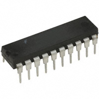


 工商网监
湘ICP备2023018690号
工商网监
湘ICP备2023018690号
