ADC0801S040
Single 8 bits ADC, up to 40 MHz
Rev. 02 — 18 August 2008
Product data sheet
1. General description
The ADC0801S040 is an 8-bit universal analog-to-digital converter (ADC) for video and
general purpose applications. It converts the analog input signal from 2.7 V to 5.5 V into
8-bit binary-coded digital words at a maximum sampling rate of 40 MHz. All digital inputs
and outputs are CMOS/Transistor-Transistor Logic (TTL) compatible. A sleep mode allows
reduction of the device power consumption to 4 mW.
2. Features
n
n
n
n
n
n
n
n
n
n
n
8-bit resolution
Operation between 2.7 V and 5.5 V
Sampling rate up to 40 MHz
DC sampling allowed
High signal-to-noise ratio over a large analog input frequency range (7.3 effective bits
at 4.43 MHz full-scale input at fclk = 40 MHz)
CMOS/TTL compatible digital inputs and outputs
External reference voltage regulator
Power dissipation only 30 mW (typical value)
Low analog input capacitance, no buffer amplifier required
Sleep mode (4 mW)
No sample-and-hold circuit required
3. Applications
n
n
n
n
n
Video data digitizing
Camera
Camcorder
Radio communication
Car alarm system
�ADC0801S040
NXP Semiconductors
Single 8 bits ADC, up to 40 MHz
4. Quick reference data
Table 1.
Quick reference data
VDDA = V5 to V6 = 3.3 V; VDDD = V3 to V4 = 3.3 V; VDDO = V20 to V11 = 3.3 V; VSSA, VSSD and VSSO
shorted together; Vi(a)(p-p) = 1.84 V; CL = 20 pF; Tamb = 0 °C to 70 °C; typical values measured at
Tamb = 25 °C unless otherwise specified.
Symbol
Parameter
Min
Typ
Max
Unit
VDDA
analog supply
voltage
Conditions
2.7
3.3
5.5
V
VDDD
digital supply
voltage
2.7
3.3
5.5
V
VDDO
output supply
voltage
2.5
3.3
5.5
V
∆VDD
supply voltage VDDA − VDDD
difference
VDDD − VDDO
−0.2
-
+0.2
V
−0.2
-
+2.25
V
IDDA
analog supply
current
-
4
6
mA
IDDD
digital supply
current
-
5
8
mA
IDDO
output supply
current
fclk = 40 MHz; ramp input;
CL = 20 pF
-
1
2
mA
INL
integral
non-linearity
ramp input; see Figure 6
-
±0.5
±0.75
LSB
DNL
differential
non-linearity
ramp input; see Figure 7
-
±0.25
±0.5
LSB
fclk(max)
maximum
clock
frequency
40
-
-
MHz
Ptot
total power
dissipation
-
30
53
mW
VDDA = VDDD = VDDO = 3.3 V
5. Ordering information
Table 2.
Ordering information
Type number
ADC0801S040TS
Package
Name
Description
Version
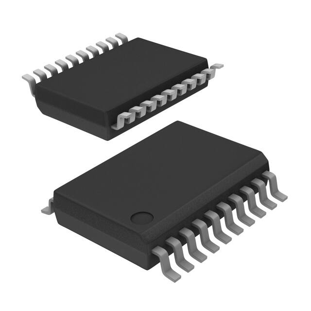
SSOP20
plastic shrink small outline package; 20 leads; body width 4.4 mm
SOT266-1
ADC0801S040_2
Product data sheet
© NXP B.V. 2008. All rights reserved.
Rev. 02 — 18 August 2008
2 of 19
�ADC0801S040
NXP Semiconductors
Single 8 bits ADC, up to 40 MHz
6. Block diagram
VDDA
CLK
VDDD
5
1
3
2
CLOCK DRIVER
RT
10
SLEEP
ADC0801S040
19 D7
MSB
18 D6
17 D5
Rlad
16 D4
analog
voltage input
VI
RM
9
ANALOG - TO - DIGITAL
CONVERTER
CMOS
OUTPUTS
LATCHES
15 D3
data outputs
14 D2
8
13 D1
12 D0
RB
20
7
6
11
4
VSSA
VSSO
VSSD
analog ground
output ground
digital ground
LSB
VDDO
014aaa495
Fig 1. Block diagram
ADC0801S040_2
Product data sheet
© NXP B.V. 2008. All rights reserved.
Rev. 02 — 18 August 2008
3 of 19
�ADC0801S040
NXP Semiconductors
Single 8 bits ADC, up to 40 MHz
7. Pinning information
7.1 Pinning
CLK
1
20 VDDO
SLEEP
2
19 D7
VDDD
3
18 D6
VSSD
4
17 D5
VDDA
5
16 D4
VSSA
6
ADC0801S
15 D3
040TS
RB
7
14 D2
RM
8
13 D1
VI
9
12 D0
RT 10
11 VSSO
014aaa494
Fig 2. Pin configuration
7.2 Pin description
Table 3.
Pin description
Symbol
Pin
Description
CLK
1
clock input
SLEEP
2
sleep mode input
VDDD
3
digital supply voltage (2.7 V to 5.5 V)
VSSD
4
digital ground
VDDA
5
analog supply voltage (2.7 V to 5.5 V)
VSSA
6
analog ground
RB
7
reference voltage BOTTOM input
RM
8
reference voltage MIDDLE
VI
9
analog input voltage
RT
10
reference voltage TOP input
VSSO
11
output stage ground
D0
12
data output; bit 0 (Least Significant Bit (LSB))
D1
13
data output; bit 1
D2
14
data output; bit 2
D3
15
data output; bit 3
D4
16
data output; bit 4
D5
17
data output; bit 5
ADC0801S040_2
Product data sheet
© NXP B.V. 2008. All rights reserved.
Rev. 02 — 18 August 2008
4 of 19
�ADC0801S040
NXP Semiconductors
Single 8 bits ADC, up to 40 MHz
Table 3.
Pin description …continued
Symbol
Pin
Description
D6
18
data output; bit 6
D7
19
data output; bit 7 (Most Significant Bit (MSB))
VDDO
20
positive supply voltage for output stage (2.7 V to 5.5 V)
8. Limiting values
Table 4.
Limiting values
In accordance with the Absolute Maximum Rating System (IEC 60134).
Symbol
Min
Max
Unit
analog supply voltage
[1]
−0.3
+7.0
V
digital supply voltage
[1]
−0.3
+7.0
V
VDDO
output supply voltage
[1]
−0.3
+7.0
V
∆VDD
supply voltage difference
VDDA − VDDD;
VDDD − VDDO;
VDDA − VDDO
−0.1
+4.0
V
VI
input voltage
referenced to
VSSA
−0.3
+7.0
V
Vi(clk)(p-p)
peak-to-peak clock input voltage referenced to
VSSD
-
VDDD
V
IO
output current
-
10
mA
Tstg
storage temperature
−55
+150
°C
Tamb
ambient temperature
−20
+75
°C
Tj
junction temperature
-
150
°C
VDDA
VDDD
[1]
Parameter
Conditions
The supply voltages VDDA, VDDD and VDDO may have any value between −0.3 V and +7.0 V provided that
the supply voltage ∆VDD remains as indicated.
9. Thermal characteristics
Table 5.
Thermal characteristics
Symbol
Parameter
Condition
Value
Unit
Rth(j-a)
thermal resistance from junction to
ambient
in free air
120
K/W
10. Characteristics
Table 6.
Characteristics
VDDA = V5 to V6 = 3.3 V; VDDD = V3 to V4 = 3.3 V; VDDO = V20 to V11 = 3.3 V; VSSA, VSSD and VSSO shorted together; Vi(a)(p-p)
= 1.84 V; CL = 20 pF; Tamb = 0 °C to 70 °C; typical values measured at Tamb = 25 °C unless otherwise specified.
Symbol
Parameter
Conditions
Min
Typ
Max
Unit
Supplies
VDDA
analog supply voltage
2.7
3.3
5.5
V
VDDD
digital supply voltage
2.7
3.3
5.5
V
VDDO
output supply voltage
2.5
3.3
5.5
ADC0801S040_2
Product data sheet
© NXP B.V. 2008. All rights reserved.
Rev. 02 — 18 August 2008
5 of 19
�ADC0801S040
NXP Semiconductors
Single 8 bits ADC, up to 40 MHz
Table 6.
Characteristics …continued
VDDA = V5 to V6 = 3.3 V; VDDD = V3 to V4 = 3.3 V; VDDO = V20 to V11 = 3.3 V; VSSA, VSSD and VSSO shorted together; Vi(a)(p-p)
= 1.84 V; CL = 20 pF; Tamb = 0 °C to 70 °C; typical values measured at Tamb = 25 °C unless otherwise specified.
Symbol
Parameter
Conditions
∆VDD
supply voltage difference VDDA − VDDD
−0.2
-
+2.25
V
IDDA
analog supply current
-
4
6
mA
IDDD
digital supply current
-
5
8
mA
IDDO
output supply current
fclk = 40 MHz; ramp input;
CL = 20 pF
-
1
2
mA
Ptot
total power dissipation
VDDA = VDDD = VDDO = 3.3 V
-
30
53
mW
VDDD − VDDO
Min
Typ
Max
Unit
−0.2
-
+0.2
V
Inputs
Clock input CLK (Referenced to VSSD)[1]
VIL
LOW-level input voltage
0
-
0.3 VDDD
V
VIH
HIGH-level input voltage VDDD ≤ 3.6 V
0.6 VDDD
-
VDDD
V
VDDD > 3.6 V
0.7 VDDD
-
VDDD
V
Vclk = 0.3 VDDD
−1
0
+1
µA
IIL
LOW-level input current
IIH
HIGH-level input current Vclk = 0.7 VDDD
-
-
5
µA
Zi
input impedance
fclk = 40 MHz
-
4
-
kΩ
Ci
input capacitance
fclk = 40 MHz
-
3
-
pF
Input SLEEP (Referenced to VSSD); see Table 8
VIL
LOW-level input voltage
0
-
0.3 VDDD
V
VIH
HIGH-level input voltage VDDD ≤ 3.6 V
0.6 VDDD
-
VDDD
V
VDDD > 3.6 V
0.7 VDDD
-
VDDD
V
VIL = 0.3 VDDD
−1
-
-
µA
-
-
+1
µA
IIL
LOW-level input current
IIH
HIGH-level input current VIH = 0.7 VDDD
Analog input VI (Referenced to VSSA)
IIL
LOW-level input current
VI = VRB
-
0
-
µA
IIH
HIGH-level input current VI = VRT
-
9
-
µA
Zi
input impedance
fi = 1 MHz
-
20
-
kΩ
Ci
input capacitance
fi = 1 MHz
-
2
-
pF
1.1
1.2
-
V
Reference voltages for the resistor ladder; see Table 7
VRB
voltage on pin RB
VRT
voltage on pin RT
VRT ≤ VDDA
2.7
3.3
VDDA
V
Vref(dif)
differential reference
voltage
VRT − VRB
1.5
2.1
2.7
V
Iref
reference current
-
0.95
-
mA
Rlad
ladder resistance
-
2.2
-
kΩ
TCRlad
ladder resistor
temperature coefficient
-
4092
-
mΩ/K
Voffset
offset voltage
Vi(a)(p-p)
peak-to-peak analog
input voltage
BOTTOM
[2]
-
170
-
mV
TOP
[2]
-
170
-
mV
[3]
1.4
1.76
2.4
V
ADC0801S040_2
Product data sheet
© NXP B.V. 2008. All rights reserved.
Rev. 02 — 18 August 2008
6 of 19
�ADC0801S040
NXP Semiconductors
Single 8 bits ADC, up to 40 MHz
Table 6.
Characteristics …continued
VDDA = V5 to V6 = 3.3 V; VDDD = V3 to V4 = 3.3 V; VDDO = V20 to V11 = 3.3 V; VSSA, VSSD and VSSO shorted together; Vi(a)(p-p)
= 1.84 V; CL = 20 pF; Tamb = 0 °C to 70 °C; typical values measured at Tamb = 25 °C unless otherwise specified.
Symbol
Parameter
Conditions
Min
Typ
Max
Unit
Digital outputs D7 to D0 and IR (Referenced to VSSD)
VOL
LOW-level output
voltage
IO = 1 mA
0
-
0.5
V
VOH
HIGH-level output
voltage
IO = −1 mA
VDDO − 0.5
-
VDDO
V
IOZ
OFF-state output current 0.4 V < VO < VDDO
−20
-
+20
µA
40
-
-
MHz
Clock input CLK; see Figure 4[1]
fclk(max)
maximum clock
frequency
tw(clk)H
HIGH clock pulse width
9
-
-
ns
tw(clk)L
LOW clock pulse width
9
-
-
ns
Analog signal processing (fclk = 40 MHz)
Linearity
INL
integral non-linearity
ramp input; see Figure 6
-
±0.5
±0.75
LSB
DNL
differential non-linearity
ramp input; see Figure 7
-
±0.25
±0.5
LSB
bandwidth
full-scale sine wave
-
10
MHz
75 % full-scale sine wave
-
13
MHz
50 % full-scale sine wave
-
20
MHz
small signal at mid scale;
Vi = ±10 LSB at code 128
-
350
MHz
Bandwidth
B
[4]
Input set response; see Figure 8[5]
ts(LH)
LOW to HIGH settling
time
full-scale square wave
-
3
5
ns
ts(HL)
HIGH to LOW settling
time
full-scale square wave
-
3
5
ns
-
−50
-
dB
without harmonics;
fi= 4.43 MHz
-
47
-
dB
fi = 300 MHz
-
7.8
-
bits
fi = 4.43 MHz
-
7.3
-
bits
PAL modulated ramp
-
1.5
-
%
Harmonics; see Figure 9[6]
THD
total harmonic distortion fi = 4.43 MHz
Signal-to-Noise ratio; see Figure
S/N
9[6]
signal-to-noise ratio
Effective bits; see Figure 9[6]
ENOB
effective number of bits
Differential gain[7]
Gdif
differential gain
ADC0801S040_2
Product data sheet
© NXP B.V. 2008. All rights reserved.
Rev. 02 — 18 August 2008
7 of 19
�ADC0801S040
NXP Semiconductors
Single 8 bits ADC, up to 40 MHz
Table 6.
Characteristics …continued
VDDA = V5 to V6 = 3.3 V; VDDD = V3 to V4 = 3.3 V; VDDO = V20 to V11 = 3.3 V; VSSA, VSSD and VSSO shorted together; Vi(a)(p-p)
= 1.84 V; CL = 20 pF; Tamb = 0 °C to 70 °C; typical values measured at Tamb = 25 °C unless otherwise specified.
Symbol
Differential
ϕdif
Parameter
Conditions
Min
Typ
Max
Unit
PAL modulated ramp
-
0.25
-
deg
phase[7]
differential phase
Timing (fclk = 40 MHz; CL = 20 pF); see Figure 4[8]
td(s)
sampling delay time
-
-
5
ns
th(o)
output hold time
5
-
-
ns
td(o)
output delay time
VDDO = 4.75 V
8
12
15
ns
VDDO = 3.15 V
8
17
20
ns
VDDO = 2.7 V
8
18
21
ns
3-state output delay times; see Figure 5
tdHZ
active HIGH to float
delay time
-
14
18
ns
tdZL
float to active LOW delay
time
-
16
20
ns
tdZH
float to active HIGH
delay time
-
16
20
ns
tdLZ
active LOW to float delay
time
-
14
18
ns
[1]
In addition to a good layout of the digital and analog ground, it is recommended that the rise and fall times of the clock must not be less
than 1 ns.
[2]
Analog input voltages producing code 0 up to and including code 255:
a) Voffset BOTTOM is the difference between the analog input which produces data equal to 00 and the reference voltage on pin RB
(VRB) at Tamb = 25 °C.
b) Voffset TOP is the difference between the reference voltage on pin RT (VRT) and the analog input which produces data outputs equal
to code 255 at Tamb = 25 °C.
[3]
To ensure the optimum linearity performance of such a converter architecture the lower and upper extremities of the converter reference
resistor ladder are connected to pins RB and RT via offset resistors ROB and ROT as shown in Figure 3.
V RT – V RB
R OB + R L + R OT
a) The current flowing into the resistor ladder is I = ---------------------------------------- and the full-scale input range at the converter, to cover code 0
RL
to 255 is V I = R L × I L = ---------------------------------------- × ( V RT + V RB ) = 0.838 × ( V RT – V RB )
R OB + R L + R OT
RL
R OB + R L + R OT
b) Since RL, ROB and ROT have similar behavior with respect to process and temperature variation, the ratio ---------------------------------------will be kept reasonably constant from device to device. Consequently variation of the output codes at a given input voltage depends
mainly on the difference VRT − VRB and its variation with temperature and supply voltage. When several ADCs are connected in
parallel and fed with the same reference source, the matching between each of them is optimized.
[4]
The analog bandwidth is defined as the maximum input sine wave frequency which can be applied to the device. No glitches greater
than 2 LSB, nor any significant attenuation is observed in the reconstructed signal.
[5]
The analog input settling time is the minimum time required for the input signal to be stabilized after a sharp full-scale input (square
wave signal) in order to sample the signal and obtain correct output data.
[6]
Effective bits are obtained via a Fast Fourier Transform (FFT) treatment taking 8000 acquisition points per equivalent fundamental
period. The calculation takes into account all harmonics and noise up to half of the clock frequency (Nyquist frequency). Conversion to
signal-to-noise ratio: S/N = ENOB × 6.02 + 1.76 dB.
[7]
Measurement carried out using video analyzer VM700A, where video analog signal is reconstructed through a DAC.
[8]
Output data acquisition: the output data is available after the maximum delay time of td(o).
ADC0801S040_2
Product data sheet
© NXP B.V. 2008. All rights reserved.
Rev. 02 — 18 August 2008
8 of 19
�ADC0801S040
NXP Semiconductors
Single 8 bits ADC, up to 40 MHz
RT
9
ROT
code 255
RL
RL
RM
7
IL
RL
Rlad
RL
code 0
ROB
RB
6
014aaa504
Fig 3. Explanation of Table 6 Table note 3
11. Additional information relating to Table 6
Table 7.
Output coding and input voltage (typical values; referenced to VSSA)
Code
Vi(a)(p-p) (V)
Binary outputs D7 to D0
Underflow
< 1.37
00 0000 00
0
1.37
00 0000 00
1
-
00 0000 01
↓
-
↓
254
-
11 11 11 10
255
3.13
11 11 11 11
Overflow
> 3.13
11 11 11 11
Table 8.
Mode selection
SLEEP
D7 to D0
IDDA + IDDD (typ)
1
high impedance
1.2 mA
0
active
9 mA
ADC0801S040_2
Product data sheet
© NXP B.V. 2008. All rights reserved.
Rev. 02 — 18 August 2008
9 of 19
�ADC0801S040
NXP Semiconductors
Single 8 bits ADC, up to 40 MHz
sample N
sample N + 1
sample N + 2
tw(clk)L
tw(clk)H
50 %
CLK
sample N
sample N + 1
sample N + 2
VI
td(s)
th(o)
VDDO
DATA
D0 to D7
DATA
N−2
DATA
N−1
DATA
N
DATA
N+1
50 %
0V
td(o)
014aaa508
Fig 4. Timing diagram
ADC0801S040_2
Product data sheet
© NXP B.V. 2008. All rights reserved.
Rev. 02 — 18 August 2008
10 of 19
�ADC0801S040
NXP Semiconductors
Single 8 bits ADC, up to 40 MHz
VDDD
50 %
SLEEP
tdHZ
tdZH
HIGH
90 %
output
data
50 %
LOW
tdZL
tdLZ
HIGH
output
data
50 %
LOW
10 %
VDDD
3.3 kΩ
ADC0801S040
S1
20 pF
SLEEP
TEST
S1
tdLZ
VDDD
tdZL
VDDD
tdHZ
GND
tdZH
GND
014aaa496
frequency on pin SLEEP = 100 kHz.
Fig 5. Timing diagram and test conditions of 3-state output delay time
014aaa501
0.291
A
(LSB)
0.178
0.065
−0.047
−0.160
−0.272
0
68
136
204
272
codes
Fig 6. Typical Integral Non-Linearity (INL) performance
ADC0801S040_2
Product data sheet
© NXP B.V. 2008. All rights reserved.
Rev. 02 — 18 August 2008
11 of 19
�ADC0801S040
NXP Semiconductors
Single 8 bits ADC, up to 40 MHz
014aaa502
0.150
A
(LSB)
0.091
0.032
−0.025
−0.84
−0.143
0
68
136
204
272
codes
Fig 7. Typical Differential Non-Linearity (DNL) performance
ts(LH)
ts(HL)
code 255
VI
50 %
50 %
code 0
5 ns
CLK
5 ns
50 %
50 %
2 ns
2 ns
014aaa497
Fig 8. Analog input settling-time diagram
ADC0801S040_2
Product data sheet
© NXP B.V. 2008. All rights reserved.
Rev. 02 — 18 August 2008
12 of 19
�ADC0801S040
NXP Semiconductors
Single 8 bits ADC, up to 40 MHz
014aaa503
0
A
(dB)
−40
−80
−120
0
5.0
10.0
15.0
20.0
f (MHz)
Effective bits: 7.32; THD = −51.08 dB.
Harmonic levels (dB): 2nd = −68.99; 3rd = −51.62; 4th = −66.05; 5th = −63.23; 6th = −72.79.
Fig 9. Typical fast Fourier transform (fclk = 40 MHz; fi = 4.43 MHz)
VDDA
VDDO
D7 to D0
VI
VSSO
VSSA
014aaa498
Fig 10. CMOS data outputs
014aaa505
Fig 11. VI analog input
VDDA
VDDO
RT
RL
RL
RM
SLEEP
RL
RL
RB
VSSO
VSSA
014aaa506
014aaa499
Fig 12. SLEEP 3-state input
Fig 13. RB, RM and RT inputs
ADC0801S040_2
Product data sheet
© NXP B.V. 2008. All rights reserved.
Rev. 02 — 18 August 2008
13 of 19
�ADC0801S040
NXP Semiconductors
Single 8 bits ADC, up to 40 MHz
VDDD
CLK
1/ V
2 DDD
VSSD
014aaa507
Fig 14. CLK input
ADC0801S040_2
Product data sheet
© NXP B.V. 2008. All rights reserved.
Rev. 02 — 18 August 2008
14 of 19
�ADC0801S040
NXP Semiconductors
Single 8 bits ADC, up to 40 MHz
12. Application information
12.1 Application diagrams
CLK
1
20
VDDO
SLEEP
2
19
D7
VDDD
3
18
D6
VSSD
4
17
D5
VDDA
5
16
D4
ADC0801S040
VSSA
RB(1)
100 nF
RM(1)
6
15
D3
7
14
D2
8
13
D1
9
12
D0
10
11
VSSO
100 nF
VSSA
VI
VSSA
RT(1)
100 nF
VSSA
014aaa500
The analog and digital supplies should be separated and decoupled.
The external voltage reference generator must be built in such a way that a good supply voltage
ripple rejection is achieved with respect to the LSB value. Eventually, the reference ladder voltages
can be derived from a well regulated VDDA supply through a resistor bridge and a decoupling
capacitor.
(1) RB, RM, RT are decoupled to VSSA.
Fig 15. Application diagram
ADC0801S040_2
Product data sheet
© NXP B.V. 2008. All rights reserved.
Rev. 02 — 18 August 2008
15 of 19
�ADC0801S040
NXP Semiconductors
Single 8 bits ADC, up to 40 MHz
13. Package outline
SSOP20: plastic shrink small outline package; 20 leads; body width 4.4 mm
D
SOT266-1
E
A
X
c
y
HE
v M A
Z
11
20
Q
A2
A
(A 3)
A1
pin 1 index
θ
Lp
L
1
10
detail X
w M
bp
e
0
2.5
5 mm
scale
DIMENSIONS (mm are the original dimensions)
UNIT
A
max.
A1
A2
A3
bp
c
D (1)
E (1)
e
HE
L
Lp
Q
v
w
y
Z (1)
θ
mm
1.5
0.15
0
1.4
1.2
0.25
0.32
0.20
0.20
0.13
6.6
6.4
4.5
4.3
0.65
6.6
6.2
1
0.75
0.45
0.65
0.45
0.2
0.13
0.1
0.48
0.18
10
o
0
o
Note
1. Plastic or metal protrusions of 0.20 mm maximum per side are not included.
OUTLINE
VERSION
SOT266-1
REFERENCES
IEC
JEDEC
JEITA
EUROPEAN
PROJECTION
ISSUE DATE
99-12-27
03-02-19
MO-152
Fig 16. Package outline SOT266-1 (SSOP20)
ADC0801S040_2
Product data sheet
© NXP B.V. 2008. All rights reserved.
Rev. 02 — 18 August 2008
16 of 19
�ADC0801S040
NXP Semiconductors
Single 8 bits ADC, up to 40 MHz
14. Revision history
Table 9.
Revision history
Document ID
Release date
Data sheet status
Change notice
Supersedes
ADC0801S040_2
20080818
Product data sheet
-
ADC0801S040_1
-
-
Modifications:
ADC0801S040_1
•
•
•
•
•
Corrections made to table notes in Figure 1.
Corrections made to Table 3.
Corrections made to symbol in Table 4.
Corrections made to Table 6.
Corrections made to Figure 13
20080612
Product data sheet
ADC0801S040_2
Product data sheet
© NXP B.V. 2008. All rights reserved.
Rev. 02 — 18 August 2008
17 of 19
�ADC0801S040
NXP Semiconductors
Single 8 bits ADC, up to 40 MHz
15. Legal information
15.1 Data sheet status
Document status[1][2]
Product status[3]
Definition
Objective [short] data sheet
Development
This document contains data from the objective specification for product development.
Preliminary [short] data sheet
Qualification
This document contains data from the preliminary specification.
Product [short] data sheet
Production
This document contains the product specification.
[1]
Please consult the most recently issued document before initiating or completing a design.
[2]
The term ‘short data sheet’ is explained in section “Definitions”.
[3]
The product status of device(s) described in this document may have changed since this document was published and may differ in case of multiple devices. The latest product status
information is available on the Internet at URL http://www.nxp.com.
15.2 Definitions
Draft — The document is a draft version only. The content is still under
internal review and subject to formal approval, which may result in
modifications or additions. NXP Semiconductors does not give any
representations or warranties as to the accuracy or completeness of
information included herein and shall have no liability for the consequences of
use of such information.
Short data sheet — A short data sheet is an extract from a full data sheet
with the same product type number(s) and title. A short data sheet is intended
for quick reference only and should not be relied upon to contain detailed and
full information. For detailed and full information see the relevant full data
sheet, which is available on request via the local NXP Semiconductors sales
office. In case of any inconsistency or conflict with the short data sheet, the
full data sheet shall prevail.
15.3 Disclaimers
General — Information in this document is believed to be accurate and
reliable. However, NXP Semiconductors does not give any representations or
warranties, expressed or implied, as to the accuracy or completeness of such
information and shall have no liability for the consequences of use of such
information.
Right to make changes — NXP Semiconductors reserves the right to make
changes to information published in this document, including without
limitation specifications and product descriptions, at any time and without
notice. This document supersedes and replaces all information supplied prior
to the publication hereof.
Suitability for use — NXP Semiconductors products are not designed,
authorized or warranted to be suitable for use in medical, military, aircraft,
space or life support equipment, nor in applications where failure or
malfunction of an NXP Semiconductors product can reasonably be expected
to result in personal injury, death or severe property or environmental
damage. NXP Semiconductors accepts no liability for inclusion and/or use of
NXP Semiconductors products in such equipment or applications and
therefore such inclusion and/or use is at the customer’s own risk.
Applications — Applications that are described herein for any of these
products are for illustrative purposes only. NXP Semiconductors makes no
representation or warranty that such applications will be suitable for the
specified use without further testing or modification.
Limiting values — Stress above one or more limiting values (as defined in
the Absolute Maximum Ratings System of IEC 60134) may cause permanent
damage to the device. Limiting values are stress ratings only and operation of
the device at these or any other conditions above those given in the
Characteristics sections of this document is not implied. Exposure to limiting
values for extended periods may affect device reliability.
Terms and conditions of sale — NXP Semiconductors products are sold
subject to the general terms and conditions of commercial sale, as published
at http://www.nxp.com/profile/terms, including those pertaining to warranty,
intellectual property rights infringement and limitation of liability, unless
explicitly otherwise agreed to in writing by NXP Semiconductors. In case of
any inconsistency or conflict between information in this document and such
terms and conditions, the latter will prevail.
No offer to sell or license — Nothing in this document may be interpreted
or construed as an offer to sell products that is open for acceptance or the
grant, conveyance or implication of any license under any copyrights, patents
or other industrial or intellectual property rights.
Quick reference data — The Quick reference data is an extract of the
product data given in the Limiting values and Characteristics sections of this
document, and as such is not complete, exhaustive or legally binding.
15.4 Trademarks
Notice: All referenced brands, product names, service names and trademarks
are the property of their respective owners.
16. Contact information
For more information, please visit: http://www.nxp.com
For sales office addresses, please send an email to: salesaddresses@nxp.com
ADC0801S040_2
Product data sheet
© NXP B.V. 2008. All rights reserved.
Rev. 02 — 18 August 2008
18 of 19
�ADC0801S040
NXP Semiconductors
Single 8 bits ADC, up to 40 MHz
17. Contents
1
2
3
4
5
6
7
7.1
7.2
8
9
10
11
12
12.1
13
14
15
15.1
15.2
15.3
15.4
16
17
General description . . . . . . . . . . . . . . . . . . . . . . 1
Features . . . . . . . . . . . . . . . . . . . . . . . . . . . . . . . 1
Applications . . . . . . . . . . . . . . . . . . . . . . . . . . . . 1
Quick reference data . . . . . . . . . . . . . . . . . . . . . 2
Ordering information . . . . . . . . . . . . . . . . . . . . . 2
Block diagram . . . . . . . . . . . . . . . . . . . . . . . . . . 3
Pinning information . . . . . . . . . . . . . . . . . . . . . . 4
Pinning . . . . . . . . . . . . . . . . . . . . . . . . . . . . . . . 4
Pin description . . . . . . . . . . . . . . . . . . . . . . . . . 4
Limiting values. . . . . . . . . . . . . . . . . . . . . . . . . . 5
Thermal characteristics. . . . . . . . . . . . . . . . . . . 5
Characteristics . . . . . . . . . . . . . . . . . . . . . . . . . . 5
Additional information relating to Table 6 . . . . 9
Application information. . . . . . . . . . . . . . . . . . 15
Application diagrams . . . . . . . . . . . . . . . . . . . 15
Package outline . . . . . . . . . . . . . . . . . . . . . . . . 16
Revision history . . . . . . . . . . . . . . . . . . . . . . . . 17
Legal information. . . . . . . . . . . . . . . . . . . . . . . 18
Data sheet status . . . . . . . . . . . . . . . . . . . . . . 18
Definitions . . . . . . . . . . . . . . . . . . . . . . . . . . . . 18
Disclaimers . . . . . . . . . . . . . . . . . . . . . . . . . . . 18
Trademarks . . . . . . . . . . . . . . . . . . . . . . . . . . . 18
Contact information. . . . . . . . . . . . . . . . . . . . . 18
Contents . . . . . . . . . . . . . . . . . . . . . . . . . . . . . . 19
Please be aware that important notices concerning this document and the product(s)
described herein, have been included in section ‘Legal information’.
© NXP B.V. 2008.
All rights reserved.
For more information, please visit: http://www.nxp.com
For sales office addresses, please send an email to: salesaddresses@nxp.com
Date of release: 18 August 2008
Document identifier: ADC0801S040_2
�


 工商网监
湘ICP备2023018690号
工商网监
湘ICP备2023018690号
