Freescale Semiconductor
Technical Data
Document Number: MPC17C724
Rev 3.0, 9/2014
0.4 A Dual H-Bridge Motor Driver
IC
17C724
The 17C724 is a SMARTMOS compact monolithic dual channel HBridge power IC, ideal for portable electronic applications containing
bipolar stepper motors or brush DC motors such as those used in
camera lenses and shutters.
The 17C724 can operate efficiently with supply voltages from 2.7 V
to 5.5 V and can provide continuous motor drive currents of 0.4 A with
low RDS(on) of 1.0 . It is easily interfaced to low cost MCUs via
parallel 3.0 V or 5.0 V compatible logic and has built-in shoot-through
current protection circuit and undervoltage detector to avoid
malfunction.
The 17C724 has four output control modes: forward, reverse,
brake, and tri-state (high-impedance). The H-Bridge outputs are
designed to be independently PWMed at up to 200 kHz for speed/
torque and current control.
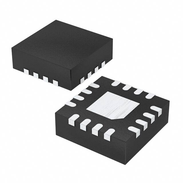
MOTOR DRIVER
EP (Pb-FREE) SUFFIX
SCALE 4:1
98ASA00741D
16-Pin QFN
ORDERING INFORMATION
Features
• Manufactured in SMOS7 process technology
• Built-in 2-channel H-Bridge driver
• Provides 4 driving modes (forward, reverse, break, highimpedance)
• Direct interface to MCU
• Low ON-Resistance, RDS(on) = 1.0 (typical)
Device
Package
R2 Suffix)
Temperature
Range (TA)
MPC17C724EP
-20 °C to 85 °C
16 QFN
(For Tape and Reel, add an
• Dual channel parallel drive, RDS(on) = 0.5 (typical)
•
•
•
•
•
•
Output current driver is 400 mA (continuous)
Low power consumption
Built-in shoot-through current prevention circuit
Built-in low voltage shutdown circuit
PWM control frequency 200 kHz (max)
Very compact size, comes in 16-pin QFN Package (3 x 3 mm pin Pitch: 0.5 mm)
3.0 V
17C724
VDD
VM
OUT1A
OUT1B
MCU
IN1A
OUT2A
IN1B
IN2A
OUT2B
S
N
Bipolar
Step
Motor
IN2B
PSAVE
GND
Figure 1. 17C724 Simplified Application Diagram
© Freescale Semiconductor, Inc., 2012-2014. All rights reserved.
�INTERNAL BLOCK DIAGRAM
INTERNAL BLOCK DIAGRAM
VDD
PSAVELowVoltage
Shutdown
VM1
IN1A
OUT1A
H-Bridge 1
OUT1B
IN1B
VDD
PSAVE
Control
Logic
PGND1
Level Shifter
Predriver
VM2
IN2A
OUT2A
H-Bridge 2
OUT2B
IN2B
PGND2
PGND2
LGND
Figure 2. 17C724 Simplified Internal Block Diagram
17C724
2
Analog Integrated Circuit Device Data
Freescale Semiconductor
�PIN CONNECTIONS
PIN CONNECTIONS
VDD
PGND1
LGND
PSAVE
Transparent Top View of Package
16
15
14
13
1N1B
2
11
IN2B
OUT1A
3
10
OUT1B
VM1
4
9
VM2
5
6
7
8
OUT2B
IN2A
PGND2
12
PGND2
1
OUT2A
1N1A
Figure 3. 17C724 Pin Connections
Table 1. 17C724 Pin Definitions
A functional description of each pin can be found in the Functional Pin Description section beginning on page 8.
Pin Number
Pin Name
Pin Function
Formal Name
Definition
1
IN1A
Logic
Logic Input Control 1A Logic input control of OUT1A (refer to Table 5, Truth Table, page 7).
2
IN1B
Logic
Logic Input Control 1B Logic input control of OUT1B (refer to Table 5, Truth Table, page 7).
3
OUT1A
Output
H-Bridge Output 1A
Output A of H-Bridge channel 1.
4
VM1
Power
Motor Driver Power
Supply 1
Positive power source connection for H-Bridge 1 (Motor Driver Power
Supply) (1).
5
OUT2A
Output
H-Bridge Output 2A
Output A of H-Bridge channel 2.
6, 7
PGND2
Ground
Power Ground 2
High-current power ground 2 (2).
8
OUT2B
Output
H-Bridge Output 2B
Output B of H-Bridge channel 2.
9
VM2
Power
Motor Driver Power
Supply 2
Positive power source connection for H-Bridge 2 (Motor Driver Power
H-Bridge Output 1B
Output B of H-Bridge channel 1.
Supply) (1).
10
OUT1B
Output
11
IN2B
Input
Logic Input Control 2B Logic input control of OUT2B (refer to Table 5, Truth Table, page 7).
12
IN2A
Input
Logic Input Control 2A Logic input control of OUT2A (refer to Table 5, Truth Table, page 7).
13
PSAVE
Input
Input Enable Control
14
LGND
Ground
Logic Ground
15
PGND1
Ground
Power Ground 1
16
VDD
Logic
Logic Circuit Power
Supply
Logic input enable control of H-Bridges to save power.
Low-current logic signal ground (2).
High-current power ground 1 (2).
Positive power source connection for logic circuit.
Notes
1. VM1 and VM2 are internally connected.
2. LGND, PGND1, and PGND2 are internally connected.
17C724
Analog Integrated Circuit Device Data
Freescale Semiconductor
3
�MAXIMUM RATINGS
MAXIMUM RATINGS
Table 2. Maximum Ratings
All voltages are with respect to ground unless otherwise noted. Exceeding these ratings may cause a malfunction or
permanent damage to the device.
Ratings
Symbol
Value
Unit
Normal Operation (Steady-State)
V M(SS)
- 0.3 to 6.0
Transient Conditions (3)
V M(PK)
- 0.3 to 6.5
Logic Supply Voltage
V DD
6.0
V
Input Pin Voltage
V IN
- 0.3 to VDD + 0.3
V
Driver Output Current (Continuous) (4)
IO
400
mA
I OPK
800
mA
Human Body Model
V ESD1
± 2000
V
Machine Model
V ESD2
± 200
T STG
- 40 to 150
C
TA
- 20 to 85
C
TJ
150 maximum
C
C/W
ELECTRICAL RATINGS
V
Power Supply Voltage (Motor Driver)
Driver Output Current (Peak) (5)
ESD Voltage (6)
TEMPERATURE RATINGS
Storage Temperature
Operating Temperature
Ambient
Operating Junction Temperature
Thermal Resistance (Junction-to-Ambient)
Single-Layer PCB Mounting (9)
Multi-Layer PCB (2S2P) Mounting
Pin Soldering Temperature (7), (8)
Notes
3.
4.
5.
6.
7.
8.
9.
10.
(10)
R JA
169
R JMA
47
TPPRT
Note 8
C
Transient condition within 500 ms.
Continuous output current must not be exceeded and at operating junction temperature below 150 C.
Peak time is for 10 ms pulse width at 200 ms intervals.
ESD testing is performed in accordance with the Human Body Model (CZAP = 100 pF, RZAP = 1500 and the Machine Model
(CZAP = 200 pF, RZAP = 0 ).
Pin soldering temperature limit is for 10 seconds maximum duration. Not designed for immersion soldering. Exceeding these limits may
cause a malfunction or permanent damage to the device.
Freescale’s Package Reflow capability meets Pb-free requirements for JEDEC standard J-STD-020C. For Peak Package Reflow
Temperature and Moisture Sensitivity Levels (MSL), Go to www.freescale.com, search by part number [e.g. remove prefixes/suffixes
and enter the core ID to view all orderable parts (i.e. MC33xxxD enter 33xxx), and review parametrics.
For cases using SEMI G38-87, JEDEC JESD51-2, JESD51-3, JESD51-5, single layer PCB mounting without thermal vias.
For cases using SEMI JEDEC JESD51-6, JESD51-5, JESD51-7, 2S2P PCB mounting with 4 thermal vias.
17C724
4
Analog Integrated Circuit Device Data
Freescale Semiconductor
�STATIC ELECTRICAL CHARACTERISTICS
STATIC ELECTRICAL CHARACTERISTICS
Table 3. Static Electrical Characteristics
Characteristics noted under conditions TA = 25 °C, VDD = VM = 3.0 V, unless otherwise noted. Typical values noted reflect the
approximate parameter means at TA = 25 °C under nominal conditions unless otherwise noted.
Characteristic
Symbol
Min
Typ
Max
Unit
Motor Driver Supply Voltage
VM
2.7
3.0
5.5
Logic Supply Voltage
V DD
2.7
3.0
5.5
VMSTBY
–
–
1.0
VDDSTBY
–
–
1.0
–
40
100
V DD 0.7
–
–
V
V DD 0.3
V
1.0
A
POWER INPUT (VDD, PSAVE)
V
Supply Voltage Range
Standby Power Supply Current (11)
I
VM = 3.0 V
I
VDD = 3.0 V
A
A
IC
Operating Power Supply Current (12)
VDD = 3.0 V
Logic Input Function
V IH
High-Level Input Voltage
Low-Level Input Voltage
V IL
–
–
High-Level Input Current
I. IH
–
–
I IL
- 1.0
–
–
A
I IL
–
- 30
- 60
A
Driver Output ON Resistance (14)
R DS(ON)
–
1.0
1.5
Low Voltage Shutdown Detection Voltage (15)
V DDDET
1.5
2.0
2.5
V
Low-Level Input Current
PSAVE Pin Low Level Input Current
(13)
Notes
11. Power SAVE mode.
12. IC is the sum of the current of V DD monitor block “Low Voltage Detection Module” and the PSAVE pull-up resistor at f IN = 200 kHz.
13.
VDD = 3.0 V.
14.
RSOURCE + RSINK at IO = 375 mA.
15.
Detection voltage is defined as when the output becomes high impedance after VDD voltage falls and when VM = 5.5 V.
17C724
Analog Integrated Circuit Device Data
Freescale Semiconductor
5
�DYNAMIC ELECTRICAL CHARACTERISTICS
DYNAMIC ELECTRICAL CHARACTERISTICS
Table 4. Dynamic Electrical Characteristics
Characteristics noted under conditions TA = 25 °C, VDD = VM = 3.0 V, unless otherwise noted. Typical values noted reflect the
approximate parameter means at TA = 25 °C under nominal conditions unless otherwise noted.
Characteristic
Symbol
Min
Typ
Max
Unit
Pulse Input Frequency
f IN
–
–
200
kHz
Input Pulse Rise Time (16)
tR
–
–
1.0
s
Input Pulse Fall Time (18)
tF
–
INPUT
(17)
–
1.0
s
(17)
OUTPUT
s
Output Propagation Delay Time (19)
Turn-ON Time
t PLH
–
0.2
0.5
Turn-OFF Time
t PHL
–
0.1
0.5
t VDDDET
–
0.02
1.0
Low-Voltage Detection Time
Notes
16.
17.
18.
19.
ms
Time is defined between 10% and 90%.
That is, the input waveform slope must be steeper than this.
Time is defined between 90% and 10%.
RL = 6.8 . Slew time, rise time, and fall times are between 10% and 90% of output low and high levels with respect to the 50% level of
the input.
17C724
6
Analog Integrated Circuit Device Data
Freescale Semiconductor
�TIMING DIAGRAMS
TIMING DIAGRAMS
IN1,
IN2,
PSAVE
VDDDETon
50%
VDD
tPLH
50%
1.0 V
tPHL
tVDDDET
tVDDDET
90%
OUTA,
OUTB
VDDDEToff
2.5 V
90%
10%
0%
(


 工商网监
湘ICP备2023018690号
工商网监
湘ICP备2023018690号
