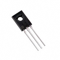
2N4918 - 2N4920 Series
Medium-Power Plastic PNP
Silicon Transistors
These medium−power, high−performance plastic devices are
designed for driver circuits, switching, and amplifier applications.
http://onsemi.com
Features
•
•
•
•
•
•
Low Saturation Voltage − VCE(sat) = 0.6 Vdc (Max) @ IC = 1.0 A
Excellent Power Dissipation, PD = 30 W @ TC = 25_C
Excellent Safe Operating Area
Gain Specified to IC = 1.0 A
Complement to NPN 2N4921, 2N4922, 2N4923
Pb−Free Package is Available*
3.0 A, 40−80 V, 30 W
GENERAL PURPOSE
POWER TRANSISTORS
MAXIMUM RATINGS
4
Rating
Symbol
Collector − Emitter Voltage
2N4918
2N4919
2N4920
Collector − Base Voltage
2N4918
2N4919
2N4920
Emitter − Base Voltage
VCEO
VCBO
Value
Unit
Vdc
40
60
80
Vdc
5.0
Vdc
IC
(Note 2)
1.0
3.0
Adc
Base Current
IB
1.0
Adc
Total Power Dissipation @ TA = 25°C
Derate above 25°C
PD
30
0.24
W
W/°C
TJ, Tstg
−65 to +150
°C
Operating and Storage Junction
Temperature Range
Stresses exceeding those listed in the Maximum Ratings table may damage
the device. If any of these limits are exceeded, device functionality should not
be assumed, damage may occur and reliability may be affected.
1. The 1.0 A max IC value is based upon JEDEC current gain requirements. The
3.0 A max value is based upon actual current−handling capability of the
device (See Figure 5).
2. Indicates JEDEC Registered Data for 2N4918 Series.
THERMAL CHARACTERISTICS (Note 3)
Characteristic
Thermal Resistance,
Junction−to−Case
FRONT VIEW
40
60
80
VEBO
Collector Current − Continuous
(Note 1)
3 2
1
1 2
3
Symbol
Max
Unit
qJC
4.16
°C/W
BACK VIEW
TO−225
CASE 077
STYLE 1
MARKING DIAGRAM
YWW
2N
49xx
xx
Y
WW
= 18, 19, 20
= Year
= Work Week
ORDERING INFORMATION
See detailed ordering and shipping information on page 2 of
this data sheet.
3. Recommend use of thermal compound for lowest thermal resistance.
*For additional information on our Pb−Free strategy and soldering details, please
download the ON Semiconductor Soldering and Mounting Techniques
Reference Manual, SOLDERRM/D.
© Semiconductor Components Industries, LLC, 2004
January, 2017 − Rev. 12
1
Publication Order Number:
2N4918/D
�2N4918 − 2N4920 Series
ÎÎÎÎÎÎÎÎÎÎÎÎÎÎÎÎÎÎÎÎÎÎÎÎÎÎÎÎÎÎÎÎÎ
ÎÎÎÎÎÎÎÎÎÎÎÎÎÎÎÎÎÎÎÎÎÎÎÎÎÎÎÎÎÎÎÎÎ
ÎÎÎÎÎÎÎÎÎÎÎÎÎÎÎÎÎÎÎÎÎÎ
ÎÎÎÎÎÎÎÎÎÎÎÎÎÎÎ
ÎÎÎÎÎÎÎÎÎÎÎÎÎÎÎÎÎÎÎÎÎÎÎÎÎÎÎÎÎÎÎÎÎÎÎÎÎ
ÎÎÎÎÎÎÎÎÎÎÎÎÎÎÎÎÎÎÎÎÎÎÎÎÎÎÎÎÎÎÎÎÎ
ÎÎÎÎÎÎÎÎÎÎÎÎÎÎÎÎÎÎÎÎÎÎÎÎÎÎÎÎÎÎÎÎÎ
ÎÎÎÎÎÎÎÎÎÎÎÎÎÎÎÎÎÎÎÎÎÎ
ÎÎÎÎÎ
ÎÎÎ
ÎÎÎÎ
ÎÎÎ
ÎÎÎÎÎÎÎÎÎÎÎÎÎÎÎÎÎÎÎÎÎÎÎÎÎÎÎÎÎÎÎÎÎÎÎÎÎ
ÎÎÎÎÎÎÎÎÎÎÎÎÎÎÎÎÎÎÎÎÎÎÎÎÎÎÎÎÎÎÎÎÎÎÎÎÎ
ÎÎÎÎÎÎÎÎÎÎÎÎÎÎÎÎÎÎÎÎÎÎÎÎÎÎÎÎÎÎÎÎÎÎÎÎÎ
ÎÎÎÎÎÎÎÎÎÎÎÎÎÎÎÎÎÎÎÎÎÎÎÎÎÎÎÎÎÎÎÎÎÎÎÎÎ
ÎÎÎÎÎÎÎÎÎÎÎÎÎÎÎÎÎÎÎÎÎÎÎÎÎÎÎÎÎÎÎÎÎÎÎÎÎ
ÎÎÎÎÎÎÎÎÎÎÎÎÎÎÎÎÎÎÎÎÎÎÎÎÎÎÎÎÎÎÎÎÎÎÎÎÎ
ÎÎÎÎÎÎÎÎÎÎÎÎÎÎÎÎÎÎÎÎÎÎ
ÎÎÎÎÎ
ÎÎÎ
ÎÎÎÎ
ÎÎÎ
ÎÎÎÎÎÎÎÎÎÎÎÎÎÎÎÎÎÎÎÎÎÎÎÎÎÎÎÎÎÎÎÎÎÎÎÎÎ
ÎÎÎÎÎÎÎÎÎÎÎÎÎÎÎÎÎÎÎÎÎÎÎÎÎÎÎÎÎÎÎÎÎÎÎÎÎ
ÎÎÎÎÎÎÎÎÎÎÎÎÎÎÎÎÎÎÎÎÎÎ
ÎÎÎÎÎ
ÎÎÎ
ÎÎÎÎ
ÎÎÎ
ÎÎÎÎÎÎÎÎÎÎÎÎÎÎÎÎÎÎÎÎÎÎÎÎÎÎÎÎÎÎÎÎÎÎÎÎÎ
ÎÎÎÎÎÎÎÎÎÎÎÎÎÎÎÎÎÎÎÎÎÎÎÎÎÎÎÎÎÎÎÎÎÎÎÎÎ
ÎÎÎÎÎÎÎÎÎÎÎÎÎÎÎÎÎÎÎÎÎÎÎÎÎÎÎÎÎÎÎÎÎ
ÎÎÎÎÎÎÎÎÎÎÎÎÎÎÎÎÎÎÎÎÎÎÎÎÎÎÎÎÎÎÎÎÎ
ÎÎÎÎÎÎÎÎÎÎÎÎÎÎÎÎÎÎÎÎÎÎ
ÎÎÎÎÎÎÎÎÎÎÎÎÎÎÎ
ÎÎÎÎÎÎÎÎÎÎÎÎÎÎÎÎÎÎÎÎÎÎ
ÎÎÎÎÎ
ÎÎÎ
ÎÎÎÎ
ÎÎÎ
ÎÎÎÎÎÎÎÎÎÎÎÎÎÎÎÎÎÎÎÎÎÎÎÎÎÎÎÎÎÎÎÎÎÎÎÎÎ
ÎÎÎÎÎÎÎÎÎÎÎÎÎÎÎÎÎÎÎÎÎÎ
ÎÎÎÎÎ
ÎÎÎ
ÎÎÎÎ
ÎÎÎ
ÎÎÎÎÎÎÎÎÎÎÎÎÎÎÎÎÎÎÎÎÎÎÎÎÎÎÎÎÎÎÎÎÎÎÎÎÎ
ÎÎÎÎÎÎÎÎÎÎÎÎÎÎÎÎÎÎÎÎÎÎ
ÎÎÎÎÎÎÎÎÎÎÎÎÎÎÎÎÎÎÎÎÎÎÎÎÎÎÎ
ÎÎÎÎÎÎÎÎ
ÎÎÎÎÎÎÎ
ÎÎÎÎÎÎÎ
ÎÎÎ
ÎÎÎÎÎÎÎÎÎÎÎÎÎÎÎÎÎÎÎÎÎÎÎÎÎÎÎÎÎÎÎÎÎÎÎÎÎ
ÎÎÎÎÎÎÎÎÎÎÎÎÎÎÎÎÎÎÎÎÎÎÎÎÎÎÎÎÎÎÎÎÎÎÎÎÎ
ÎÎÎÎÎÎÎÎÎÎÎÎÎÎÎÎÎÎÎÎÎÎÎÎÎÎÎÎÎÎÎÎÎ
ÎÎÎÎÎÎÎÎÎÎÎÎÎÎÎÎÎÎÎÎÎÎÎÎÎÎÎÎÎÎÎÎÎ
ÎÎÎÎÎÎÎÎÎÎÎÎÎÎÎÎÎÎÎÎÎÎ
ÎÎÎÎÎÎÎÎÎÎÎÎÎÎÎ
ÎÎÎÎÎÎÎÎÎÎÎÎÎÎÎÎÎÎÎÎÎÎÎÎÎÎÎÎÎÎÎÎÎÎÎÎÎ
ÎÎÎÎÎÎÎÎÎÎÎÎÎÎÎÎÎÎÎÎÎÎ
ÎÎÎÎÎÎÎÎÎÎÎÎÎÎÎÎÎÎÎÎÎÎÎÎÎÎÎ
ÎÎÎÎÎÎÎÎ
ÎÎÎÎÎÎÎ
ÎÎÎÎÎÎÎ
ÎÎÎ
ELECTRICAL CHARACTERISTICS (TC = 25_C unless otherwise noted)
Characteristic
Symbol
Min
Max
40
60
80
−
−
−
−
−
−
0.5
0.5
0.5
−
−
0.1
0.5
Unit
OFF CHARACTERISTICS
Collector−Emitter Sustaining Voltage (Note 4)
(IC = 0.1 Adc, IB = 0)
2N4918
2N4919
2N4920
Collector Cutoff Current
(VCE = 20 Vdc, IB = 0)
(VCE = 30 Vdc, IB = 0)
(VCE = 40 Vdc, IB = 0)
2N4918
2N4919
2N4920
VCEO(sus)
ICEO
Vdc
mAdc
Collector Cutoff Current
(VCE = Rated VCEO, VBE(off) = 1.5 Vdc)
(VCE = Rated VCEO, VBE(off) = 1.5 Vdc, TC = 125_C
ICEX
mAdc
Collector Cutoff Current
(VCB = Rated VCB, IE = 0)
ICBO
−
0.1
mAdc
Emitter Cutoff Current
(VBE = 5.0 Vdc, IC = 0)
IEBO
−
1.0
mAdc
40
30
10
−
150
−
ON CHARACTERISTICS
DC Current Gain (Note 4)
(IC = 50 mAdc, VCE = 1.0 Vdc)
(IC = 500 mAdc, VCE = 1.0 Vdc)
(IC = 1.0 Adc, VCE = 1.0 Vdc)
hFE
−
Collector−Emitter Saturation Voltage (Note 4)
(IC = 1.0 Adc, IB = 0.1 Adc)
VCE(sat)
−
0.6
Vdc
Base−Emitter Saturation Voltage (Note 4)
(IC = 1.0 Adc, IB = 0.1 Adc)
VBE(sat)
−
1.3
Vdc
Base−Emitter On Voltage (Note 4)
(IC = 1.0 Adc, VCE = 1.0 Vdc)
VBE(on)
−
1.3
Vdc
SMALL−SIGNAL CHARACTERISTICS
Current−Gain − Bandwidth Product (IC = 250 mAdc, VCE = 10 Vdc, f = 1.0 MHz)
fT
3.0
−
MHz
Output Capacitance (VCB = 10 Vdc, IE = 0, f = 100 kHz)
Cob
−
100
pF
Small−Signal Current Gain (IC = 250 mAdc, VCE = 10 Vdc, f = 1.0 kHz)
hfe
25
−
−
4. Pulse Test: PW [ 300 ms, Duty Cycle [ 2.0%
ORDERING INFORMATION
Package
Shipping†
2N4918
TO−225
500 Unit / Bulk
2N4919
TO−225
500 Unit / Bulk
2N4920
TO−225
500 Unit / Bulk
TO−225
(Pb−Free)
500 Unit / Bulk
Device
2N4920G
†For information on tape and reel specifications, including part orientation and tape sizes, please refer to our Tape and Reel Packaging Specifications Brochure, BRD8011/D.
www.onsemi.com
2
�2N4918 − 2N4920 Series
PD, POWER DISSIPATION (WATTS)
40
30
20
10
0
25
50
75
100
TC, CASE TEMPERATURE (°C)
125
150
Figure 1. Power Derating
VBE(off)
5.0
0
APPROX
-11 V
VCC
Vin
t1
RC
t2
Vin
RB
APPROX
-11 V
0
t1 < 15 ns
100 < t2 < 500 ms
t3 < 15 ns
t3
TURN-OFF PULSE
IC/IB = 10, UNLESS NOTED
TJ = 25°C
TJ = 150°C
2.0
SCOPE
Cjd�
