BAV99W, BAV99RW
Dual Series Switching
Diodes
The BAV99WT1G is a smaller package, equivalent to the
BAV99LT1G.
www.onsemi.com
Features
• S and NSV Prefix for Automotive and Other Applications Requiring
•
Unique Site and Control Change Requirements; AEC−Q101
Qualified and PPAP Capable
These Devices are Pb−Free, Halogen Free/BFR Free and are RoHS
Compliant*
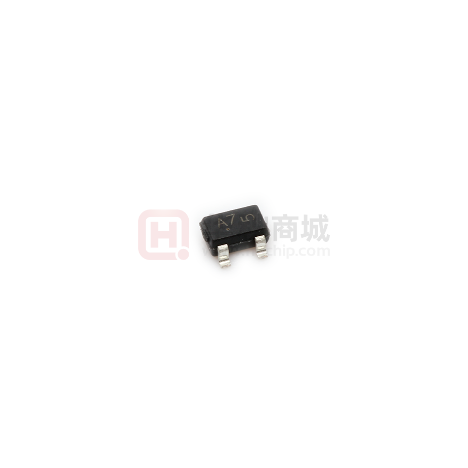
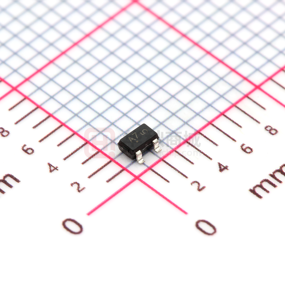
SC−70
CASE 419
ANODE
1
Suggested Applications
•
•
•
•
•
ESD Protection
Polarity Reversal Protection
Data Line Protection
Inductive Load Protection
Steering Logic
CATHODE
2
3
CATHODE/ANODE
BAV99WT1
SC−70, CASE 419, STYLE 9
CATHODE
1
ANODE
2
MAXIMUM RATINGS (Each Diode)
Rating
3
CATHODE/ANODE
Symbol
Value
Unit
Reverse Voltage
VR
100
Vdc
Forward Current
IF
215
mAdc
BAV99RWT1
SC−70, CASE 419, STYLE 10
MARKING DIAGRAM
Peak Forward Surge Current
IFM(surge)
500
mAdc
Repetitive Peak Reverse Voltage
VRRM
100
V
Average Rectified Forward Current
(Note 1)
(averaged over any 20 ms period)
IF(AV)
715
mA
Repetitive Peak Forward Current
IFRM
450
mA
Non−Repetitive Peak Forward Current
t = 1.0 ms
t = 1.0 ms
t = 1.0 s
IFSM
X7 MG
G
1
A7
F7
M
G
= BAV99W
= BAV99RW
= Date Code
= Pb−Free Package
A
2.0
1.0
0.5
ORDERING INFORMATION
Package
Shipping†
BAV99WT1G
SC−70
(Pb−Free)
3,000 / Tape & Reel
SBAV99WT1G
SC−70
(Pb−Free)
3,000 / Tape & Reel
BAV99RWT1G
SC−70
(Pb−Free)
3,000 / Tape & Reel
SBAV99RWT1G
SC−70
(Pb−Free)
3,000 / Tape & Reel
NSVBAV99WT3G
SC−70
10,000 / Tape & Reel
(Pb−Free)
Device
Stresses exceeding those listed in the Maximum Ratings table may damage the
device. If any of these limits are exceeded, device functionality should not be
assumed, damage may occur and reliability may be affected.
1. FR−5 = 1.0 � 0.75 � 0.062 in.
†For information on tape and reel specifications,
including part orientation and tape sizes, please
refer to our Tape and Reel Packaging Specifications
Brochure, BRD8011/D.
© Semiconductor Components Industries, LLC, 2015
November, 2017 − Rev. 10
1
Publication Order Number:
BAV99WT1/D
�BAV99W, BAV99RW
THERMAL CHARACTERISTICS
Characteristic
Symbol
Max
Unit
PD
200
1.6
mW
mW/°C
RqJA
625
°C/W
PD
300
2.4
mW
mW/°C
RqJA
417
°C/W
TJ, Tstg
−65 to +150
°C
Total Device Dissipation FR−5 Board, (Note 1) TA = 25°C
Derate above 25°C
Thermal Resistance Junction−to−Ambient
Total Device Dissipation Alumina Substrate, (Note 2) TA = 25°C
Derate above 25°C
Thermal Resistance Junction−to−Ambient
Junction and Storage Temperature
ELECTRICAL CHARACTERISTICS (TA = 25°C unless otherwise noted) (Each Diode)
Symbol
Characteristic
Min
Max
100
−
−
−
−
1.0
30
50
−
1.5
−
−
−
−
715
855
1000
1250
−
6.0
−
1.75
Unit
OFF CHARACTERISTICS
Reverse Breakdown Voltage
(I(BR) = 100 mA)
V(BR)
Reverse Voltage Leakage Current
(VR = 100 Vdc)
(VR = 25 Vdc, TJ = 150°C)
(VR = 70 Vdc, TJ = 150°C)
IR
Diode Capacitance
(VR = 0, f = 1.0 MHz)
CD
Forward Voltage
(IF = 1.0 mAdc)
(IF = 10 mAdc)
(IF = 50 mAdc)
(IF = 150 mAdc)
VF
Reverse Recovery Time
(IF = IR = 10 mAdc, iR(REC) = 1.0 mAdc) (Figure 1) RL = 100 W
trr
Forward Recovery Voltage
(IF = 10 mA, tr = 20 ns)
Vdc
mAdc
pF
mVdc
ns
VFR
V
Product parametric performance is indicated in the Electrical Characteristics for the listed test conditions, unless otherwise noted. Product
performance may not be indicated by the Electrical Characteristics if operated under different conditions.
1. FR−5 = 1.0 � 0.75 � 0.062 in.
2. Alumina = 0.4 � 0.3 � 0.024 in. 99.5% alumina.
820 W
+10 V
2k
100 mH
0.1 mF
IF
tr
tp
0.1 mF
t
IF
trr
10%
t
DUT
50 W OUTPUT
PULSE
GENERATOR
90%
50 W INPUT
SAMPLING
OSCILLOSCOPE
IR
VR
INPUT SIGNAL
Notes: (a) A 2.0 kW variable resistor adjusted for a Forward Current (IF) of 10 mA.
Notes: (b) Input pulse is adjusted so IR(peak) is equal to 10 mA.
Notes: (c) tp » trr
Figure 1. Recovery Time Equivalent Test Circuit
www.onsemi.com
2
iR(REC) = 1 mA
OUTPUT PULSE
(IF = IR = 10 mA; measured
at iR(REC) = 1 mA)
�BAV99W, BAV99RW
CURVES APPLICABLE TO EACH DIODE
1000
10
I R, REVERSE CURRENT (��A)
μ
100
10
TA = 150°C TA = 25°C
1.0
TA = -�55°C
TA = 125°C
1.0
TA = 85°C
0.1
TA = 55°C
0.01
TA = 25°C
0.1
0.0
0.2
0.4
0.6
0.8
VF, FORWARD VOLTAGE (VOLTS)
1.0
0.001
1.2
10
0
Figure 2. Forward Voltage
20
30
40
VR, REVERSE VOLTAGE (VOLTS)
Figure 3. Leakage Current
0.68
CD , DIODE CAPACITANCE (pF)
IF, FORWARD CURRENT (mA)
TA = 150°C
0.64
0.60
0.56
0.52
0
2
4
6
VR, REVERSE VOLTAGE (VOLTS)
Figure 4. Capacitance
www.onsemi.com
3
8
50
�BAV99W, BAV99RW
PACKAGE DIMENSIONS
SC−70 (SOT−323)
CASE 419−04
ISSUE N
D
NOTES:
1. DIMENSIONING AND TOLERANCING PER ANSI Y14.5M, 1982.
2. CONTROLLING DIMENSION: INCH.
e1
3
DIM
A
A1
A2
b
c
D
E
e
e1
L
HE
E
HE
1
2
b
e
A
0.05 (0.002)
0.30
0.10
1.80
1.15
1.20
0.20
2.00
MILLIMETERS
NOM
MAX
0.90
1.00
0.05
0.10
0.70 REF
0.35
0.40
0.18
0.25
2.10
2.20
1.24
1.35
1.30
1.40
0.65 BSC
0.38
0.56
2.10
2.40
MIN
0.032
0.000
0.012
0.004
0.071
0.045
0.047
0.008
0.079
INCHES
NOM
0.035
0.002
0.028 REF
0.014
0.007
0.083
0.049
0.051
0.026 BSC
0.015
0.083
MAX
0.040
0.004
0.016
0.010
0.087
0.053
0.055
0.022
0.095
c
A2
STYLE 9:
PIN 1. ANODE
2. CATHODE
3. CATHODE-ANODE
L
A1
MIN
0.80
0.00
STYLE 10:
PIN 1. CATHODE
2. ANODE
3. ANODE-CATHODE
SOLDERING FOOTPRINT*
0.65
0.025
0.65
0.025
1.9
0.075
0.9
0.035
0.7
0.028
SCALE 10:1
mm Ǔ
ǒinches
*For additional information on our Pb−Free strategy and soldering
details, please download the ON Semiconductor Soldering and
Mounting Techniques Reference Manual, SOLDERRM/D.
ON Semiconductor and
are trademarks of Semiconductor Components Industries, LLC dba ON Semiconductor or its subsidiaries in the United States and/or other countries.
ON Semiconductor owns the rights to a number of patents, trademarks, copyrights, trade secrets, and other intellectual property. A listing of ON Semiconductor’s product/patent
coverage may be accessed at www.onsemi.com/site/pdf/Patent−Marking.pdf. ON Semiconductor reserves the right to make changes without further notice to any products herein.
ON Semiconductor makes no warranty, representation or guarantee regarding the suitability of its products for any particular purpose, nor does ON Semiconductor assume any liability
arising out of the application or use of any product or circuit, and specifically disclaims any and all liability, including without limitation special, consequential or incidental damages.
Buyer is responsible for its products and applications using ON Semiconductor products, including compliance with all laws, regulations and safety requirements or standards,
regardless of any support or applications information provided by ON Semiconductor. “Typical” parameters which may be provided in ON Semiconductor data sheets and/or
specifications can and do vary in different applications and actual performance may vary over time. All operating parameters, including “Typicals” must be validated for each customer
application by customer’s technical experts. ON Semiconductor does not convey any license under its patent rights nor the rights of others. ON Semiconductor products are not
designed, intended, or authorized for use as a critical component in life support systems or any FDA Class 3 medical devices or medical devices with a same or similar classification
in a foreign jurisdiction or any devices intended for implantation in the human body. Should Buyer purchase or use ON Semiconductor products for any such unintended or unauthorized
application, Buyer shall indemnify and hold ON Semiconductor and its officers, employees, subsidiaries, affiliates, and distributors harmless against all claims, costs, damages, and
expenses, and reasonable attorney fees arising out of, directly or indirectly, any claim of personal injury or death associated with such unintended or unauthorized use, even if such
claim alleges that ON Semiconductor was negligent regarding the design or manufacture of the part. ON Semiconductor is an Equal Opportunity/Affirmative Action Employer. This
literature is subject to all applicable copyright laws and is not for resale in any manner.
PUBLICATION ORDERING INFORMATION
LITERATURE FULFILLMENT:
Literature Distribution Center for ON Semiconductor
19521 E. 32nd Pkwy, Aurora, Colorado 80011 USA
Phone: 303−675−2175 or 800−344−3860 Toll Free USA/Canada
Fax: 303−675−2176 or 800−344−3867 Toll Free USA/Canada
Email: orderlit@onsemi.com
◊
N. American Technical Support: 800−282−9855 Toll Free
USA/Canada
Europe, Middle East and Africa Technical Support:
Phone: 421 33 790 2910
Japan Customer Focus Center
Phone: 81−3−5817−1050
www.onsemi.com
4
ON Semiconductor Website: www.onsemi.com
Order Literature: http://www.onsemi.com/orderlit
For additional information, please contact your local
Sales Representative
BAV99WT1/D
�


 工商网监
湘ICP备2023018690号
工商网监
湘ICP备2023018690号
