ON Semiconductor
Is Now
To learn more about onsemi™, please visit our website at
www.onsemi.com
onsemi and and other names, marks, and brands are registered and/or common law trademarks of Semiconductor Components Industries, LLC dba “onsemi” or its affiliates and/or
subsidiaries in the United States and/or other countries. onsemi owns the rights to a number of patents, trademarks, copyrights, trade secrets, and other intellectual property. A listing of onsemi
product/patent coverage may be accessed at www.onsemi.com/site/pdf/Patent-Marking.pdf. onsemi reserves the right to make changes at any time to any products or information herein, without
notice. The information herein is provided “as-is” and onsemi makes no warranty, representation or guarantee regarding the accuracy of the information, product features, availability, functionality,
or suitability of its products for any particular purpose, nor does onsemi assume any liability arising out of the application or use of any product or circuit, and specifically disclaims any and all
liability, including without limitation special, consequential or incidental damages. Buyer is responsible for its products and applications using onsemi products, including compliance with all laws,
regulations and safety requirements or standards, regardless of any support or applications information provided by onsemi. “Typical” parameters which may be provided in onsemi data sheets and/
or specifications can and do vary in different applications and actual performance may vary over time. All operating parameters, including “Typicals” must be validated for each customer application
by customer’s technical experts. onsemi does not convey any license under any of its intellectual property rights nor the rights of others. onsemi products are not designed, intended, or authorized
for use as a critical component in life support systems or any FDA Class 3 medical devices or medical devices with a same or similar classification in a foreign jurisdiction or any devices intended for
implantation in the human body. Should Buyer purchase or use onsemi products for any such unintended or unauthorized application, Buyer shall indemnify and hold onsemi and its officers, employees,
subsidiaries, affiliates, and distributors harmless against all claims, costs, damages, and expenses, and reasonable attorney fees arising out of, directly or indirectly, any claim of personal injury or death
associated with such unintended or unauthorized use, even if such claim alleges that onsemi was negligent regarding the design or manufacture of the part. onsemi is an Equal Opportunity/Affirmative
Action Employer. This literature is subject to all applicable copyright laws and is not for resale in any manner. Other names and brands may be claimed as the property of others.
�BUZ11
Data Sheet
September 2013
N-Channel Power MOSFET
50V, 30A, 40 mΩ
Features
This is an N-Channel enhancement mode silicon gate power
field effect transistor designed for applications such as
switching regulators, switching converters, motor drivers,
relay drivers and drivers for high power bipolar switching
transistors requiring high speed and low gate drive power.
This type can be operated directly from integrated circuits.
• rDS(ON) = 0.040Ω
File Number
2253.2
• 30A, 50V
• SOA is Power Dissipation Limited
• Nanosecond Switching Speeds
• Linear Transfer Characteristics
• High Input Impedance
Formerly developmental type TA9771.
• Majority Carrier Device
Ordering Information
PART NUMBER
BUZ11-NR4941
PACKAGE
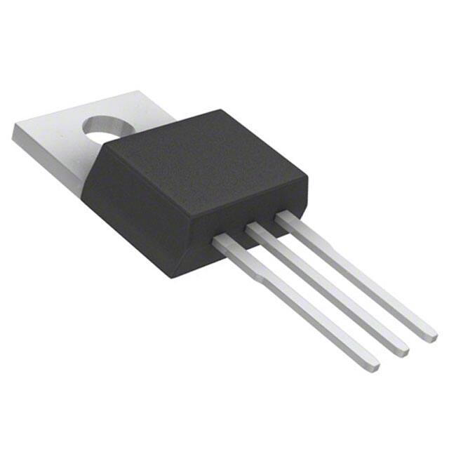
TO-220AB
• Related Literature
- TB334 “Guidelines for Soldering Surface Mount
Components to PC Boards”
BRAND
BUZ11
Symbol
NOTE: When ordering, use the entire part number.
D
G
S
Packaging
JEDEC TO-220AB
SOURCE
DRAIN
GATE
DRAIN (FLANGE)
©2001 Semiconductor Components Industries, LLC.
October-2017, Rev. 3
Publication Order Number:
BUZ11/D
�BUZ11
Absolute Maximum Ratings
TC = 25oC, Unless Otherwise Specified
BUZ11
UNITS
50
50
30
V
V
A
Gate to Source Voltage . . . . . . . . . . . . . . . . . . . . . . . . . . . . . . . . . . . . . . . . . . . . . . . . . . . . . . . .VGS
Maximum Power Dissipation . . . . . . . . . . . . . . . . . . . . . . . . . . . . . . . . . . . . . . . . . . . . . . . . . . . . .PD
Linear Derating Factor . . . . . . . . . . . . . . . . . . . . . . . . . . . . . . . . . . . . . . . . . . . . . . . . . . . . . . . . . . . .
Operating and Storage Temperature . . . . . . . . . . . . . . . . . . . . . . . . . . . . . . . . . . . . . . . . . . TJ, TSTG
DIN Humidity Category - DIN 40040 . . . . . . . . . . . . . . . . . . . . . . . . . . . . . . . . . . . . . . . . . . . . . . . . .
IEC Climatic Category - DIN IEC 68-1. . . . . . . . . . . . . . . . . . . . . . . . . . . . . . . . . . . . . . . . . . . . . . . .
120
±20
75
0.6
-55 to 150
E
55/150/56
A
V
W
W/oC
oC
Maximum Temperature for Soldering
Leads at 0.063in (1.6mm) from Case for 10s. . . . . . . . . . . . . . . . . . . . . . . . . . . . . . . . . . . . . . . TL
Package Body for 10s, See Techbrief 334 . . . . . . . . . . . . . . . . . . . . . . . . . . . . . . . . . . . . . . . Tpkg
300
260
oC
oC
Drain to Source Breakdown Voltage (Note 1) . . . . . . . . . . . . . . . . . . . . . . . . . . . . . . . . . . . . . . .VDS
Drain to Gate Voltage (RGS = 20kΩ) (Note 1) . . . . . . . . . . . . . . . . . . . . . . . . . . . . . . . . . . . . . VDGR
Continuous Drain Current TC = 30oC. . . . . . . . . . . . . . . . . . . . . . . . . . . . . . . . . . . . . . . . . . . . . ID
Pulsed Drain Current (Note 3) . . . . . . . . . . . . . . . . . . . . . . . . . . . . . . . . . . . . . . . . . . . . . . . . . . . IDM
CAUTION: Stresses above those listed in “Absolute Maximum Ratings” may cause permanent damage to the device. This is a stress only rating and operation of the
device at these or any other conditions above those indicated in the operational sections of this specification is not implied.
NOTE:
1. TJ = 25oC to 125oC.
Electrical Specifications
TC = 25oC, Unless Otherwise Specified
PARAMETER
SYMBOL
TEST CONDITIONS
MIN
TYP
MAX
UNITS
Drain to Source Breakdown Voltage
BVDSS
ID = 250µA, VGS = 0V
50
-
-
V
Gate Threshold Voltage
VGS(TH)
VGS = VDS, ID = 1mA (Figure 9)
2.1
3
4
V
IDSS
TJ = 25oC, VDS = 50V, VGS = 0V
-
20
250
µA
TJ = 125oC, VDS = 50V, VGS = 0V
-
100
1000
µA
VGS = 20V, VDS = 0V
-
10
100
nA
Zero Gate Voltage Drain Current
Gate to Source Leakage Current
Drain to Source On Resistance (Note 2)
Forward Transconductance (Note 2)
Turn-On Delay Time
IGSS
rDS(ON)
ID = 15A, VGS = 10V (Figure 8)
-
0.03
0.04
Ω
gfs
VDS = 25V, ID = 15A (Figure 11)
4
8
-
S
VCC = 30V, ID ≈ 3A, VGS = 10V, RGS = 50Ω,
RL = 10Ω
-
30
45
ns
-
70
110
ns
td(OFF)
-
180
230
ns
tf
-
130
170
ns
-
1500
2000
pF
pF
td(ON)
Rise Time
tr
Turn-Off Delay Time
Fall Time
Input Capacitance
CISS
Output Capacitance
COSS
-
750
1100
Reverse Transfer Capacitance
CRSS
-
250
400
VDS = 25V, VGS = 0V, f = 1MHz (Figure 10)
pF
Thermal Resistance Junction to Case
RθJC
≤ 1.67
oC/W
Thermal Resistance Junction to Ambient
RθJA
≤ 75
oC/W
Source to Drain Diode Specifications
PARAMETER
Continuous Source to Drain Current
SYMBOL
ISD
Pulsed Source to Drain Current
ISDM
Source to Drain Diode Voltage
VSD
Reverse Recovery Time
Reverse Recovery Charge
trr
QRR
TEST CONDITIONS
TC = 25oC
TC = 25oC
TJ = 25oC, ISD = 60A, VGS = 0V
TJ = 25oC, ISD = 30A, dISD/dt = 100A/µs,
VR = 30V
MIN
TYP
UNITS
-
-
30
A
-
-
120
A
-
1.7
2.6
V
-
200
-
ns
-
0.25
-
µC
NOTES:
2. Pulse Test: Pulse width ≤ 300ms, duty cycle ≤ 2%.
3. Repetitive rating: pulse width limited by maximum junction temperature. See Transient Thermal Impedance curve (Figure 3).
www.onsemi.com
2
MAX
�BUZ11
Typical Performance Curves
Unless Otherwise Specified
40
POWER DISSIPATION MULTIPLIER
1.2
VGS > 10V
ID, DRAIN CURRENT (A)
1.0
0.8
0.6
0.4
30
20
10
0.2
0
0
25
50
75
100
TA , CASE TEMPERATURE (oC)
125
ZθJC, TRANSIENT THERMAL IMPEDANCE
FIGURE 1. NORMALIZED POWER DISSIPATION vs CASE
TEMPERATURE
1
0
150
0
50
100
TC, CASE TEMPERATURE (oC)
150
FIGURE 2. MAXIMUM CONTINUOUS DRAIN CURRENT vs
CASE TEMPERATURE
0.5
0.2
0.1
0.1
PDM
0.05
0.02
0.01
t1
t2
NOTES:
DUTY FACTOR: D = t1/t2
PEAK TJ = PDM x ZθJC + TC
SINGLE PULSE
0.01
10-5
10-4
10-3
10-2
10-1
t, RECTANGULAR PULSE DURATION (s)
100
101
FIGURE 3. MAXIMUM TRANSIENT THERMAL IMPEDANCE
60
PD = 75W
OPERATION IN THIS
AREA MAY BE LIMITED
BY rDS(ON)
2.5µs
102
10µs
100µs
101
1ms
TC = 25oC
TJ = MAX RATED
SINGLE PULSE
100
100
101
VDS, DRAIN TO SOURCE VOLTAGE (V)
VGS = 20V
PULSE DURATION = 80µs
DUTY CYCLE = 0.5% MAX
50
ID, DRAIN CURRENT (A)
ID, DRAIN CURRENT (A)
103
10V
40
VGS = 8.0V
VGS = 7.5V
VGS = 7.0V
VGS = 6.5V
30
20
VGS = 6.0V
VGS = 5.5V
VGS = 5.0V
VGS = 4.5V
VGS = 4.0V
10
10ms
100ms
DC
102
0
0
FIGURE 4. FORWARD BIAS SAFE OPERATING AREA
1
2
3
4
5
VDS, DRAIN TO SOURCE VOLTAGE (V)
FIGURE 5. OUTPUT CHARACTERISTICS
www.onsemi.com
3
6
�BUZ11
20
Unless Otherwise Specified (Continued)
0.15
PULSE DURATION = 80µs
DUTY CYCLE = 0.5% MAX
VDS = 25V
rDS(ON), ON-STATE RESISTANCE (Ω)
IDS(ON), DRAIN TO SOURCE CURRENT (A)
Typical Performance Curves
15
10
5
0
0
1
2
3
4
5
6
VGS, GATE TO SOURCE VOLTAGE (V)
7
0.06
0.04
0.02
50
100
150
VDS = VGS
ID = 1mA
3
2
1
0
-50
gfs, TRANSCONDUCTANCE (S)
C, CAPACITANCE (nF)
10
CISS
COSS
CRSS
10-1
VGS = 0V, f = 1MHz
CISS = CGS + CGD
CRSS = CGD
COSS ≈ CDS + CGD
10
20
30
60
0
50
100
150
FIGURE 9. GATE THRESHOLD VOLTAGE vs JUNCTION
TEMPERATURE
101
0
20
40
ID, DRAIN CURRENT (A)
TJ, JUNCTION TEMPERATURE (oC)
FIGURE 8. DRAIN TO SOURCE ON RESISTANCE vs
JUNCTION TEMPERATURE
10-2
0
4
TJ, JUNCTION TEMPERATURE (oC)
100
10V
20V
0
VGS(TH), GATE THRESHOLD VOLTAGE (V)
rDS(ON), DRAIN TO SOURCE
ON RESISTANCE (Ω)
PULSE DURATION = 80µs
DUTY CYCLE = 0.5% MAX
ID = 15A, VGS = 10V
0
0.05
FIGURE 7. DRAIN TO SOURCE ON RESISTANCE vs GATE
VOLTAGE AND DRAIN CURRENT
0.08
-50
5.5V
6V
6.5V
7V
7.5V
8V
9V
0.10
8
FIGURE 6. TRANSFER CHARACTERISTICS
0
PULSE DURATION = 80µs
DUTY CYCLE = 0.5% MAX
VGS = 5V
40
8
TJ = 25oC
6
4
2
0
0
VDS, DRAIN TO SOURCE VOLTAGE (V)
FIGURE 10. CAPACITANCE vs DRAIN TO SOURCE VOLTAGE
PULSE DURATION = 80µs
DUTY CYCLE = 0.5% MAX
VDS = 25V
5
10
ID, DRAIN CURRENT (A)
15
FIGURE 11. TRANSCONDUCTANCE vs DRAIN CURRENT
www.onsemi.com
4
20
�BUZ11
Typical Performance Curves
15
PULSE DURATION = 80µs
DUTY CYCLE = 0.5% MAX
TJ = 25oC
102
TJ = 150oC
101
100
10-1
0
0.5
1.0
1.5
2.0
2.5
VSD, SOURCE TO DRAIN VOLTAGE (V)
ID = 45A
VGS, GATE TO SOURCE VOLTAGE (V)
ISD, SOURCE TO DRAIN CURRENT (A)
103
Unless Otherwise Specified (Continued)
VDS = 10V
10
VDS = 40V
5
0
3.0
FIGURE 12. SOURCE TO DRAIN DIODE VOLTAGE
0
10
20
30
Qg, GATE CHARGE (nC)
40
50
FIGURE 13. GATE TO SOURCE VOLTAGE vs GATE CHARGE
Test Circuits and Waveforms
tON
tOFF
td(ON)
td(OFF)
tf
tr
VDS
RL
90%
90%
+
RG
-
VDD
10%
0
10%
90%
DUT
VGS
VGS
0
FIGURE 15. RESISTIVE SWITCHING WAVEFORMS
VDS
(ISOLATED
SUPPLY)
CURRENT
REGULATOR
0.2µF
50%
PULSE WIDTH
10%
FIGURE 14. SWITCHING TIME TEST CIRCUIT
12V
BATTERY
50%
VDD
Qg(TOT)
SAME TYPE
AS DUT
50kΩ
Qgd
0.3µF
VGS
Qgs
D
VDS
DUT
G
0
Ig(REF)
S
0
IG CURRENT
SAMPLING
RESISTOR
VDS
ID CURRENT
SAMPLING
RESISTOR
Ig(REF)
0
FIGURE 16. GATE CHARGE TEST CIRCUIT
FIGURE 17. GATE CHARGE WAVEFORMS
www.onsemi.com
5
�ON Semiconductor and
are trademarks of Semiconductor Components Industries, LLC dba ON Semiconductor or its subsidiaries in the United States and/or other countries.
ON Semiconductor owns the rights to a number of patents, trademarks, copyrights, trade secrets, and other intellectual property. A listing of ON Semiconductor’s product/patent
coverage may be accessed at www.onsemi.com/site/pdf/Patent−Marking.pdf. ON Semiconductor reserves the right to make changes without further notice to any products herein.
ON Semiconductor makes no warranty, representation or guarantee regarding the suitability of its products for any particular purpose, nor does ON Semiconductor assume any liability
arising out of the application or use of any product or circuit, and specifically disclaims any and all liability, including without limitation special, consequential or incidental damages.
Buyer is responsible for its products and applications using ON Semiconductor products, including compliance with all laws, regulations and safety requirements or standards,
regardless of any support or applications information provided by ON Semiconductor. “Typical” parameters which may be provided in ON Semiconductor data sheets and/or
specifications can and do vary in different applications and actual performance may vary over time. All operating parameters, including “Typicals” must be validated for each customer
application by customer’s technical experts. ON Semiconductor does not convey any license under its patent rights nor the rights of others. ON Semiconductor products are not
designed, intended, or authorized for use as a critical component in life support systems or any FDA Class 3 medical devices or medical devices with a same or similar classification
in a foreign jurisdiction or any devices intended for implantation in the human body. Should Buyer purchase or use ON Semiconductor products for any such unintended or unauthorized
application, Buyer shall indemnify and hold ON Semiconductor and its officers, employees, subsidiaries, affiliates, and distributors harmless against all claims, costs, damages, and
expenses, and reasonable attorney fees arising out of, directly or indirectly, any claim of personal injury or death associated with such unintended or unauthorized use, even if such
claim alleges that ON Semiconductor was negligent regarding the design or manufacture of the part. ON Semiconductor is an Equal Opportunity/Affirmative Action Employer. This
literature is subject to all applicable copyright laws and is not for resale in any manner.
PUBLICATION ORDERING INFORMATION
LITERATURE FULFILLMENT:
Literature Distribution Center for ON Semiconductor
19521 E. 32nd Pkwy, Aurora, Colorado 80011 USA
Phone: 303−675−2175 or 800−344−3860 Toll Free USA/Canada
Fax: 303−675−2176 or 800−344−3867 Toll Free USA/Canada
Email: orderlit@onsemi.com
❖
© Semiconductor Components Industries, LLC
N. American Technical Support: 800−282−9855 Toll Free
USA/Canada
Europe, Middle East and Africa Technical Support:
Phone: 421 33 790 2910
Japan Customer Focus Center
Phone: 81−3−5817−1050
ON Semiconductor Website: www.onsemi.com
Order Literature: http://www.onsemi.com/orderlit
For additional information, please contact your local
Sales Representative
www.onsemi.com
�


 工商网监
湘ICP备2023018690号
工商网监
湘ICP备2023018690号
