CAT871, CAT872
Dual Input Reset Generator
Description
CAT871, CAT872 are dual input reset generators designed to restart
microprocessor and microcontroller based systems when the
watchdog timer or other resetting mechanisms have become disabled
or failed.
CAT871, CAT872 monitor two inputs and output an active low reset
pulse after both inputs have been active (logic low) for a factory preset
minimum time. The reset pulse width is 2.2 ms for CAT871 and 70 ms
for CAT872. Releasing either input from its active state before the
minimum timeout period resets the internal timer and both inputs must
return to being active before the timer will restart with a fresh count
down.
CAT871, CAT872’s open drain output is capable of sinking up to
3 mA of current and may be wire−OR’d with other open drain devices
to drive a common reset input.
http://onsemi.com
1
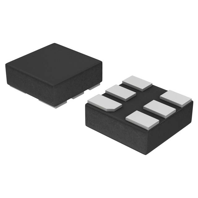
ULLGA−6
UL SUFFIX
CASE 613AF
MARKING DIAGRAM
Features
•
•
•
•
•
•
Operate on 1.65 V to 5.5 V Power Supplies
Ultra Low Quiescent Current: 10 nA (typical)
Schmitt Trigger Inputs
8 Factory Preset Delay Times from 0.5 s to 5 s to Choose From
Small mLLGA−6 Package: 1.45 x 1.0 x 0.4 mm
These Devices are Pb−Free, Halogen Free/BFR Free and are RoHS
Compliant
Typical Applications
•
•
•
•
XM
X = Specific Device Code
X = (J = CAT871, K = CAT872)
M = Date Code
PIN CONNECTIONS
MR1
Mobile Phones
PDAs
MP3 Players
Personal Navigation Devices
1
VDD
RESET
MR2
GND
NIC
(Top View)
ORDERING INFORMATION
See detailed ordering and shipping information in the package
dimensions section on page 9 of this data sheet.
Figure 1. Application Schematic
© Semiconductor Components Industries, LLC, 2011
November, 2011 − Rev. 0
1
Publication Order Number:
CAT871/D
�CAT871, CAT872
FUNCTIONAL BLOCK DIAGRAM
VDD
RESET
MR2
RESET
Pulse
Generator
Delay Timer
MR1
GND
Figure 2. Functional Block Diagram
Table 1. PIN FUNCTION DESCRIPTION
Pin No.
Pin Name
Description
1
MR1
Manual reset input #1. CMOS input.
2
MR2
Manual reset input #2. CMOS input.
3
NIC
No Internal Connection. A voltage or signal applied to this pin will have no effect on device operation.
4
GND
System Ground.
5
RESET
6
VDD
Reset Output. Active−low open drain output.
Positive Power Supply.
Table 2. ABSOLUTE MAXIMUM RATINGS
Rating
Symbol
Value
Unit
Input Voltage Range
VDD
−0.3 to 6
V
Output Voltage Range
VOUT
−0.3 to 6
or (VDD + 0.3), whichever is lower
V
VIN
−0.3 to 6
or (VDD + 0.3), whichever is lower
V
TJ(max)
150
°C
Output Current; RESET
IOUT
10
mA
Storage Temperature Range
TSTG
−65 to 150
°C
ESD Capability, Human Body Model (Note 1)
ESDHBM
2
kV
ESD Capability, Machine Model (Note 1)
ESDMM
200
V
TSLD
260
°C
Input Voltage; MR2, MR1
Maximum Junction Temperature
Lead Temperature Soldering
Reflow (SMD Styles Only), Pb−Free Versions (Note 2)
Stresses exceeding Maximum Ratings may damage the device. Maximum Ratings are stress ratings only. Functional operation above the
Recommended Operating Conditions is not implied. Extended exposure to stresses above the Recommended Operating Conditions may affect
device reliability.
1. This device series incorporates ESD protection and is tested by the following methods:
ESD Human Body Model tested per AEC−Q100−002 (EIA/JESD22−A114)
ESD Machine Model tested per AEC−Q100−003 (EIA/JESD22−A115)
Latch−up Current Maximum Rating: ≤150 mA per JEDEC standard: JESD78
2. For information, please refer to our Soldering and Mounting Techniques Reference Manual, SOLDERRM/D
http://onsemi.com
2
�CAT871, CAT872
Table 3. RECOMMENDED OPERATING CONDITIONS
Rating
Symbol
Min
Max
Unit
Input Voltage; VDD
VDD
1.65
5.5
V
Input Voltage; MR1, MR2
VIN
0
VDD
V
Output Current; RESET
IOUT
0
3
mA
TA
−40
85
°C
Ambient Temperature
Table 4. ELECTRICAL OPERATING CHARACTERISTICS
(VDD = 1.65 V to 5.5 V. For typical values TA = 25°C, for min/max values TA = −40°C to +85°C unless otherwise noted.)
Test Conditions
Parameter
Symbol
Min
VDD
1.65
Typ
Max
Unit
5.5
V
10
1000
nA
50
mA
POWER
VDD Supply Voltage
IDD
Quiescent Supply Current
MR1 = MR2 = VDD.
Operating Supply Current
MR1 = MR2 = 0 V
Measured during setup period. Measurement
includes current through internal 200 kΩ
pull−up resistor on MR2
LOGIC INPUTS AND OUTPUTS
Input Voltage; HIGH
MR1, MR2
VIH
Input Voltage; LOW
MR1, MR2
VIL
Hysteresis
VHYS
0.7 x VDD
V
0.25xVDD
−
250
Input Current
MR1 = 0 V; VDD = 5 V (no internal pull−up)
IPU
50
Input Current
MR2 = 0 V; VDD = 5 V
(internal 200 kW pull−up resistor)
IPU
25
Output Voltage; HIGH
External 10 kW pull−up resistor to VDD
VOH
Output Voltage; LOW
ISINK = 3 mA, VDD = 1.8 V
VOL
V
mV
300
nA
mA
VDD – 0.1
V
0.1
0.4
V
0.41
0.50
0.59
s
CAT87x−10
0.82
1.00
1.18
s
CAT87x−15
1.23
1.50
1.77
s
CAT87x−20
1.64
2.00
2.36
s
CAT87x−25
2.05
2.50
2.95
s
CAT87x−30
2.46
3.00
3.54
s
CAT87x−40
3.28
4.00
4.72
s
CAT87x−50
4.1
5.00
5.9
s
1.8
2.2
2.6
ms
57
70
83
TIMING
Timeout
Reset Output Pulse Width
tLOW_DELAY
CAT87x−05
tR
CAT871
CAT872
TEST MODE (at TA = 25°C) (Note 3)
tST
Start TEST window
35
ms
Test Mode delay
MR1=0 V, MR2→8 cycles, delay measured
after 8th rising edge of the MR2 clock pulse
tD
250
ms
Test Mode Clock Frequency
Clock applied to MR2
ftm
1
MHz
MR2 Test mode clock setup
time
Measured from MR1 falling edge to first
falling edge of MR2
tP
MR2 Input Voltage; LOW
MR2, Test mode operation
1
ms
VIL_TM
MR2 Pulse Width
tpw
3. “Test Mode” parameters are not tested in production.
http://onsemi.com
3
0.2xVDD
500
V
ns
�CAT871, CAT872
TIMING WAVEFORMS (Note 4)
Figure 3. Timing Waveforms
4. The order of the MR inputs going low does not matter. The last input to go low marks the beginning of tLOW_DELAY
1.75
1.75
1.70
1.70
1.65
1.65
1.60
1.50
25°C
1.45
90°C
tLOW_DELAY (s)
−40°C
1.55
1.40
1.60
1.55
1.45
1.30
1.25
1.30
1.25
−50
2
3
4
6
5
3.2 V
1.40
1.35
1
5.6 V
1.50
1.35
1.6 V
−25
0
25
50
75
100
125 150
VDD (V)
TEMPERATURE (°C)
Figure 4. tLOW_DELAY vs. VDD (CAT87x−1.5)
Figure 5. tLOW_DELAY vs. Temperature
(CAT87x−1.5)
3.5
3.4
3.3
tLOW_DELAY (s)
tLOW_DELAY (s)
TYPICAL CHARACTERISTICS
3.2
3.1
−40°C
3.0
25°C
2.9
90°C
2.8
2.7
2.6
2.5
0
1
2
3
4
5
VDD (V)
Figure 6. tLOW_DELAY vs. VDD (CAT87x−3.0)
http://onsemi.com
4
6
�CAT871, CAT872
TYPICAL CHARACTERISTICS
30
25
25
20
IMR2 (mA)
IDD (mA)
20
15
85°C
10
25°C
5
1
2
3
4
5
0
6
3
4
5
Figure 7. IDD vs. VDD (MR1 = MR2 = 0)
Figure 8. IMR2 @ MR2 = 0
2.6
2.5
2.5
2.4
2.4
−40°C
2.2
25°C
6
2.3
tR (ms)
2.3
2.1
85°C
2.2
5.6 V
2.1
3.2 V
2.0
1.6 V
1.9
1.9
1.8
2
VDD (V)
2.6
2.0
1
VDD (V)
1
2
3
5
4
1.8
−50
6
−25
0
25
50
75
100
125
VDD (V)
TEMPERATURE (°C)
Figure 9. tR vs. VDD for CAT871
Figure 10. tR vs. Temperature for CAT871
tR (ms)
tR (ms)
0
10
−40°C
5
0
15
83
81
79
77
75
73
71
69
67
65
63
61
59
57
−40°C
25°C
90°C
0
1
2
3
4
5
VDD (V)
Figure 11. Reset Pulse Width for CAT872
http://onsemi.com
5
6
150
�CAT871, CAT872
SYSTEM DESCRIPTION AND APPLICATIONS INFORMATION
General
Reset Output
CAT871, CAT872 are designed for the manual resetting of
microprocessors and microcontrollers when normal
resetting mechanisms have failed. To prevent accidental
resets, CAT871, CAT872 require both manual reset inputs
be held low for a prescribed period before a reset pulse is
issued to the system processor.
CAT871, CAT872 provide an active−low open drain
output to be wire−OR’d with other open drain reset devices.
This output will sink up to 3 mA and as such will not be
loaded down by low value (strong) pull−up resistors. The
reset pulse is typically 2 ms long for CAT871 and 70 ms long
for CAT872 and is issued at the conclusion of the delay
timer’s countdown sequence.
CAT871, CAT872 will not generate a reset pulse at
power−up.
Manual Reset Inputs
MR1 and MR2 are Schmitt trigger CMOS inputs. Both
inputs must go low and stay low for a predetermined period
(tLOW_DELAY) to generate a single reset pulse on the output.
MR1 and MR2 operate independently and may be brought
low at any time and in any order. The last input to reach 0 V
starts the delay timer.
MR1 is a standard CMOS input and MR2 is also a CMOS
input with an internal 200 kW pull−up resistor, thus MR2 can
be left floating whereas MR1 must be biased by a pull−up
resistor, powered switch or some other means external to the
IC. (Consult factory for other input biasing options)
Delay Timer Testing
To aid in−circuit testing of the delay timer, a special test
function has been included in CAT871, CAT872. This test
mode, TOC, allows the delay timer to clock at an accelerated
rate. Upon the conclusion of the countdown a standard width
reset pulse will be issued and the chip will exit test mode.
To initiate TOC, MR1→ 0 V and a fast external CLK
(typically 1 MHz) is applied on MR2, with the falling edge
of the first clock pulse on MR2 delayed with tP from MR1→
0 V. CAT871, CAT872 look for 8 sequential pulses to appear
on MR2 within 35 ms to confirm TOC is desired. After the
rising edge of the 8’th pulse, there will be a delay of 250 ms
typical followed by a standard reset pulse at the reset output.
This delay is independent of the normal timeout delay
setting.
After issuing the reset pulse, CAT871, CAT872 exit TOC
mode and returns to normal operation. If at any time during
TOC both MR1 and MR2 are HIGH, CAT871, CAT872 will
immediately exit TOC mode.
Delay Timer
When both MR1 and MR2 go low, an internal timing cycle
is initiated. If any input goes high before the countdown
timer has concluded its cycle, the timer will reset and will
restart from the beginning when MR1 and MR2 return to
being low.
If both manual reset inputs (MR1 and MR2) remain low
after a reset pulse is issued, no second reset pulse will be
issued after that.
Figure 12. TOC Mode
http://onsemi.com
6
�CAT871, CAT872
APPLICATION INFORMATION
Reset Pulse Operation
than the VDD rail (1.8 V). MR1 and MR2 inputs are
activated here by two separate switches connected to GND
and pulling the inputs low when pressed. The Schottky diode
provides the supply isolation needed between the
CAT871/CAT872 (VDD) and the microcontroller (VBAT).
When both MR1 and MR2 inputs are kept low, a single
reset pulse is generated after the delay tLOW_DELAY. Even
with both MR1 and MR2 maintained low continuously after
that time, no second reset pulse will be generated. The delay
timer restarts if either MR1 or MR2 (or both) input
transitions from high to low, as shown in the timing diagram
in Figure 13.
Operation with Low VDD Voltage and Brownout
Condition
The CAT871, CAT872 reset generators require a
minimum supply voltage VDD of 1.65 V to guarantee the
normal operation within the specification. To prevent small
VDD supply glitch, a small ceramic capacitor can be added
between the VDD pin and GND.
System with Two Different Power Supply Voltages
The reset generator can be used in a system where the
supply VDD is different than the MR1, MR2 input logic.
Figure 14 shows an application schematic where the
microcontroller uses a supply VBAT (3.6 V) that is higher
Figure 13. Reset Timing Diagram
Figure 14. Application Schematic in Dual Supply System
http://onsemi.com
7
�CAT871, CAT872
PACKAGE DIMENSIONS
ULLGA6, 1.45x1.0, 0.5P
CASE 613AF−01
ISSUE A
PIN ONE
REFERENCE
0.10 C
NOTES:
1. DIMENSIONING AND TOLERANCING PER
ASME Y14.5M, 1994.
2. CONTROLLING DIMENSION: MILLIMETERS.
3. DIMENSION b APPLIES TO PLATED TERMINAL
AND IS MEASURED BETWEEN 0.15 AND
0.30 mm FROM THE TERMINAL TIP.
4. A MAXIMUM OF 0.05 PULL BACK OF THE
PLATED TERMINAL FROM THE EDGE OF THE
PACKAGE IS ALLOWED.
A
B
D
ÉÉÉ
ÉÉÉ
ÉÉÉ
E
DIM
A
A1
b
D
E
e
L
L1
TOP VIEW
0.10 C
0.05 C
MILLIMETERS
MIN
MAX
−−−
0.40
0.00
0.05
0.15
0.25
1.45 BSC
1.00 BSC
0.50 BSC
0.25
0.35
0.30
0.40
A
6X
0.05 C
SEATING
PLANE
SIDE VIEW
MOUNTING FOOTPRINT
SOLDERMASK DEFINED*
C
A1
5X
0.49
e
5X
L
6X
0.30
NOTE 4
3
1
L1
1.24
6
4
BOTTOM VIEW
6X
0.53
b
0.10 C A B
0.05 C
1
PKG
OUTLINE
0.50
PITCH
DIMENSIONS: MILLIMETERS
NOTE 3
*For additional information on our Pb−Free strategy and soldering
details, please download the ON Semiconductor Soldering and
Mounting Techniques Reference Manual, SOLDERRM/D.
http://onsemi.com
8
�MECHANICAL CASE OUTLINE
PACKAGE DIMENSIONS
ULLGA6, 1.45x1.0, 0.5P
CASE 613AF−01
ISSUE A
1
SCALE 8:1
PIN ONE
REFERENCE
0.10 C
NOTES:
1. DIMENSIONING AND TOLERANCING PER
ASME Y14.5M, 1994.
2. CONTROLLING DIMENSION: MILLIMETERS.
3. DIMENSION b APPLIES TO PLATED TERMINAL
AND IS MEASURED BETWEEN 0.15 AND
0.30 mm FROM THE TERMINAL TIP.
4. A MAXIMUM OF 0.05 PULL BACK OF THE
PLATED TERMINAL FROM THE EDGE OF THE
PACKAGE IS ALLOWED.
A
B
D
ÉÉÉ
ÉÉÉ
DATE 06 FEB 2008
E
DIM
A
A1
b
D
E
e
L
L1
TOP VIEW
0.10 C
0.05 C
MILLIMETERS
MIN
MAX
−−−
0.40
0.00
0.05
0.15
0.25
1.45 BSC
1.00 BSC
0.50 BSC
0.25
0.35
0.30
0.40
A
6X
0.05 C
SEATING
PLANE
SIDE VIEW
C
A1
MOUNTING FOOTPRINT
SOLDERMASK DEFINED*
5X
0.49
e
5X
L
6X
0.30
NOTE 4
3
1
L1
1.24
6
4
BOTTOM VIEW
DOCUMENT NUMBER:
DESCRIPTION:
6X
b
0.10 C A B
0.05 C
NOTE 3
98AON24011D
ULLGA6, 1.45X1.0, 0.5P
0.53
1
PKG
OUTLINE
0.50
PITCH
DIMENSIONS: MILLIMETERS
*For additional information on our Pb−Free strategy and soldering
details, please download the ON Semiconductor Soldering and
Mounting Techniques Reference Manual, SOLDERRM/D.
Electronic versions are uncontrolled except when accessed directly from the Document Repository.
Printed versions are uncontrolled except when stamped “CONTROLLED COPY” in red.
PAGE 1 OF 1
ON Semiconductor and
are trademarks of Semiconductor Components Industries, LLC dba ON Semiconductor or its subsidiaries in the United States and/or other countries.
ON Semiconductor reserves the right to make changes without further notice to any products herein. ON Semiconductor makes no warranty, representation or guarantee regarding
the suitability of its products for any particular purpose, nor does ON Semiconductor assume any liability arising out of the application or use of any product or circuit, and specifically
disclaims any and all liability, including without limitation special, consequential or incidental damages. ON Semiconductor does not convey any license under its patent rights nor the
rights of others.
© Semiconductor Components Industries, LLC, 2019
www.onsemi.com
�onsemi,
, and other names, marks, and brands are registered and/or common law trademarks of Semiconductor Components Industries, LLC dba “onsemi” or its affiliates
and/or subsidiaries in the United States and/or other countries. onsemi owns the rights to a number of patents, trademarks, copyrights, trade secrets, and other intellectual property.
A listing of onsemi’s product/patent coverage may be accessed at www.onsemi.com/site/pdf/Patent−Marking.pdf. onsemi reserves the right to make changes at any time to any
products or information herein, without notice. The information herein is provided “as−is” and onsemi makes no warranty, representation or guarantee regarding the accuracy of the
information, product features, availability, functionality, or suitability of its products for any particular purpose, nor does onsemi assume any liability arising out of the application or use
of any product or circuit, and specifically disclaims any and all liability, including without limitation special, consequential or incidental damages. Buyer is responsible for its products
and applications using onsemi products, including compliance with all laws, regulations and safety requirements or standards, regardless of any support or applications information
provided by onsemi. “Typical” parameters which may be provided in onsemi data sheets and/or specifications can and do vary in different applications and actual performance may
vary over time. All operating parameters, including “Typicals” must be validated for each customer application by customer’s technical experts. onsemi does not convey any license
under any of its intellectual property rights nor the rights of others. onsemi products are not designed, intended, or authorized for use as a critical component in life support systems
or any FDA Class 3 medical devices or medical devices with a same or similar classification in a foreign jurisdiction or any devices intended for implantation in the human body. Should
Buyer purchase or use onsemi products for any such unintended or unauthorized application, Buyer shall indemnify and hold onsemi and its officers, employees, subsidiaries, affiliates,
and distributors harmless against all claims, costs, damages, and expenses, and reasonable attorney fees arising out of, directly or indirectly, any claim of personal injury or death
associated with such unintended or unauthorized use, even if such claim alleges that onsemi was negligent regarding the design or manufacture of the part. onsemi is an Equal
Opportunity/Affirmative Action Employer. This literature is subject to all applicable copyright laws and is not for resale in any manner.
PUBLICATION ORDERING INFORMATION
LITERATURE FULFILLMENT:
Email Requests to: orderlit@onsemi.com
onsemi Website: www.onsemi.com
◊
TECHNICAL SUPPORT
North American Technical Support:
Voice Mail: 1 800−282−9855 Toll Free USA/Canada
Phone: 011 421 33 790 2910
Europe, Middle East and Africa Technical Support:
Phone: 00421 33 790 2910
For additional information, please contact your local Sales Representative
�


 工商网监
湘ICP备2023018690号
工商网监
湘ICP备2023018690号
