Is Now Part of
To learn more about ON Semiconductor, please visit our website at
www.onsemi.com
Please note: As part of the Fairchild Semiconductor integration, some of the Fairchild orderable part numbers
will need to change in order to meet ON Semiconductor’s system requirements. Since the ON Semiconductor
product management systems do not have the ability to manage part nomenclature that utilizes an underscore
(_), the underscore (_) in the Fairchild part numbers will be changed to a dash (-). This document may contain
device numbers with an underscore (_). Please check the ON Semiconductor website to verify the updated
device numbers. The most current and up-to-date ordering information can be found at www.onsemi.com. Please
email any questions regarding the system integration to Fairchild_questions@onsemi.com.
ON Semiconductor and the ON Semiconductor logo are trademarks of Semiconductor Components Industries, LLC dba ON Semiconductor or its subsidiaries in the United States and/or other countries. ON Semiconductor owns the rights to a number
of patents, trademarks, copyrights, trade secrets, and other intellectual property. A listing of ON Semiconductor’s product/patent coverage may be accessed at www.onsemi.com/site/pdf/Patent-Marking.pdf. ON Semiconductor reserves the right
to make changes without further notice to any products herein. ON Semiconductor makes no warranty, representation or guarantee regarding the suitability of its products for any particular purpose, nor does ON Semiconductor assume any liability
arising out of the application or use of any product or circuit, and specifically disclaims any and all liability, including without limitation special, consequential or incidental damages. Buyer is responsible for its products and applications using ON
Semiconductor products, including compliance with all laws, regulations and safety requirements or standards, regardless of any support or applications information provided by ON Semiconductor. “Typical” parameters which may be provided in ON
Semiconductor data sheets and/or specifications can and do vary in different applications and actual performance may vary over time. All operating parameters, including “Typicals” must be validated for each customer application by customer’s
technical experts. ON Semiconductor does not convey any license under its patent rights nor the rights of others. ON Semiconductor products are not designed, intended, or authorized for use as a critical component in life support systems or any FDA
Class 3 medical devices or medical devices with a same or similar classification in a foreign jurisdiction or any devices intended for implantation in the human body. Should Buyer purchase or use ON Semiconductor products for any such unintended
or unauthorized application, Buyer shall indemnify and hold ON Semiconductor and its officers, employees, subsidiaries, affiliates, and distributors harmless against all claims, costs, damages, and expenses, and reasonable attorney fees arising out
of, directly or indirectly, any claim of personal injury or death associated with such unintended or unauthorized use, even if such claim alleges that ON Semiconductor was negligent regarding the design or manufacture of the part. ON Semiconductor
is an Equal Opportunity/Affirmative Action Employer. This literature is subject to all applicable copyright laws and is not for resale in any manner.
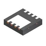
�FDMC8462
N-Channel Power Trench
®
tm
MOSFET
40V, 20A, 5.8mΩ
Features
General Description
Max rDS(on) = 5.8mΩ at VGS = 10V, ID = 13.5A
This N-Channel MOSFET is produced using Fairchild
Semiconductor‘s advanced Power Trench® process that has
been especially tailored to minimize the on-state resistance and
yet maintain superior switching performance.
Max rDS(on) = 8.0mΩ at VGS = 4.5V, ID = 11.8A
Low Profile - 1mm max in Power 33
100% UIL Tested
RoHS Compliant
Application
DC - DC Conversion
Pin 1
S
S
S
D
5
4
G
D
6
3
S
D
7
2
S
D
8
1
S
G
D
D
D
D
Bottom
Top
Power 33
MOSFET Maximum Ratings TA = 25°C unless otherwise noted
Symbol
VDS
Drain to Source Voltage
Parameter
VGS
Gate to Source Voltage
Drain Current -Continuous (Package limited)
ID
TC = 25°C
-Continuous (Silicon limited)
TC = 25°C
-Continuous
TA = 25°C
PD
TJ, TSTG
Units
V
±20
V
20
64
(Note 1a)
14
(Note 3)
216
-Pulsed
A
50
Single Pulse Avalanche Energy
EAS
Ratings
40
Power Dissipation
TC = 25°C
Power Dissipation
TA = 25°C
41
(Note 1a)
Operating and Storage Junction Temperature Range
2.0
-55 to +150
mJ
W
°C
Thermal Characteristics
RθJC
Thermal Resistance, Junction to Case
3
RθJA
Thermal Resistance, Junction to Ambient
(Note 1a)
53
°C/W
Package Marking and Ordering Information
Device Marking
FDMC8462
Device
FDMC8462
©2008 Fairchild Semiconductor Corporation
FDMC8462 Rev.C
Package
Power 33
1
Reel Size
13’’
Tape Width
12mm
Quantity
3000 units
www.fairchildsemi.com
FDMC8462 N-Channel Power Trench® MOSFET
March 2008
�Symbol
Parameter
Test Conditions
Min
Typ
Max
Units
Off Characteristics
BVDSS
Drain to Source Breakdown Voltage
ID = 250µA, VGS = 0V
∆BVDSS
∆TJ
Breakdown Voltage Temperature
Coefficient
40
V
ID = 250µA, referenced to 25°C
IDSS
Zero Gate Voltage Drain Current
VGS = 0V, VDS = 32V,
1
µA
IGSS
Gate to Source Leakage Current
VGS = ±20V, VDS = 0V
±100
nA
3.0
V
31
mV/°C
On Characteristics
VGS(th)
Gate to Source Threshold Voltage
VGS = VDS, ID = 250µA
∆VGS(th)
∆TJ
Gate to Source Threshold Voltage
Temperature Coefficient
ID = 250µA, referenced to 25°C
-6.6
VGS = 10V, ID = 13.5A
4.7
5.8
rDS(on)
Static Drain to Source On Resistance
VGS = 4.5V, ID = 11.8A
6.4
8.0
VGS = 10V, ID = 13.5A, TJ = 125°C
7.1
9.3
VDD = 5V, ID = 13.5A
60
gFS
Forward Transconductance
1.0
2.0
mV/°C
mΩ
S
Dynamic Characteristics
Ciss
Input Capacitance
Coss
Output Capacitance
Crss
Reverse Transfer Capacitance
Rg
Gate Resistance
VDS = 20V, VGS = 0V,
f = 1MHz
f = 1MHz
2000
2660
pF
545
725
pF
80
120
pF
Ω
2.7
Switching Characteristics
td(on)
Turn-On Delay Time
12
21
ns
tr
Rise Time
4
10
ns
td(off)
Turn-Off Delay Time
27
43
ns
tf
Fall Time
3
10
ns
Qg
Total Gate Charge
VGS = 0V to 10V
30
43
nC
Qg
Total Gate Charge
21
nC
Gate to Source Charge
VGS = 0V to 4.5V VDD = 20V,
ID = 13.5A
15
Qgs
Qgd
Gate to Drain “Miller” Charge
VDD = 20V, ID = 13.5A,
VGS = 10V, RGEN = 6Ω
6
nC
5
nC
Drain-Source Diode Characteristics
VSD
Source to Drain Diode Forward Voltage
trr
Reverse Recovery Time
Qrr
Reverse Recovery Charge
VGS = 0V, IS = 13.5A
(Note 2)
0.8
1.3
VGS = 0V, IS = 1.7A
(Note 2)
0.7
1.2
35
57
ns
20
32
nC
IF = 13.5A, di/dt = 100A/µs
V
NOTES:
1. RθJA is determined with the device mounted on a 1in2 pad 2 oz copper pad on a 1.5 x 1.5 in. board of FR-4 material. RθJC is guaranteed by design while RθCA is determined by
the user's board design.
a. 53°C/W when mounted on a
1 in2 pad of 2 oz copper
b. 125°C/W when mounted on a
minimum pad of 2 oz copper
2. Pulse Test: Pulse Width < 300µs, Duty cycle < 2.0%.
3. Starting TJ = 25oC; N-ch: L = 3 mH, IAS = 12A, VDD = 40V, VGS = 10V
FDMC8462 Rev.C
2
www.fairchildsemi.com
FDMC8462 N-Channel Power Trench® MOSFET
Electrical Characteristics TJ = 25°C unless otherwise noted
�5.0
NORMALIZED
DRAIN TO SOURCE ON-RESISTANCE
50
VGS = 10V
ID, DRAIN CURRENT (A)
40
VGS = 3.5V
VGS = 4.5V
30
VGS = 4V
20
PULSE DURATION = 80µs
DUTY CYCLE = 0.5%MAX
10
VGS = 3V
0
0.0
0.5
1.0
VGS = 3V
4.0
3.5
VGS = 3.5V
3.0
2.5
VGS = 4V
2.0
1.5
1.0
1.5
0
10
20
30
40
50
ID, DRAIN CURRENT(A)
Figure 1. On-Region Characteristics
Figure 2. Normalized On-Resistance
vs Drain Current and Gate Voltage
30
ID = 13.5A
VGS = 10V
rDS(on), DRAIN TO
1.6
1.4
1.2
1.0
0.8
0.6
-75
SOURCE ON-RESISTANCE (mΩ)
1.8
NORMALIZED
DRAIN TO SOURCE ON-RESISTANCE
VGS = 10V
VGS = 4.5V
0.5
VDS, DRAIN TO SOURCE VOLTAGE (V)
ID = 13.5A
25
PULSE DURATION = 80µs
DUTY CYCLE = 0.5%MAX
20
15
TJ = 125oC
10
5
TJ = 25oC
0
-50
-25
0
25
50
75
2
100 125 150
TJ, JUNCTION TEMPERATURE (oC)
4
6
8
10
VGS, GATE TO SOURCE VOLTAGE (V)
Figure 3. Normalized On- Resistance
vs Junction Temperature
Figure 4. On-Resistance vs Gate to
Source Voltage
50
50
IS, REVERSE DRAIN CURRENT (A)
PULSE DURATION = 80µs
DUTY CYCLE = 0.5%MAX
40
ID, DRAIN CURRENT (A)
PULSE DURATION = 80µs
DUTY CYCLE = 0.5%MAX
4.5
VDS = 5V
30
TJ = 150oC
20
TJ = 25oC
10
TJ =
-55oC
2
3
4
TJ = 150oC
1
TJ = 25oC
0.1
0.01
TJ = -55oC
0.001
0.0
0
1
VGS = 0V
10
5
0.2
0.4
0.6
0.8
1.0
VGS, GATE TO SOURCE VOLTAGE (V)
VSD, BODY DIODE FORWARD VOLTAGE (V)
Figure 5. Transfer Characteristics
Figure 6. Source to Drain Diode
Forward Voltage vs Source Current
FDMC8462 Rev.C
3
1.2
www.fairchildsemi.com
FDMC8462 N-Channel Power Trench® MOSFET
Typical Characteristics TJ = 25°C unless otherwise noted
�5000
ID = 13.5A
VDD = 16V
8
CAPACITANCE (pF)
VGS, GATE TO SOURCE VOLTAGE(V)
10
VDD = 20V
6
VDD = 24V
4
Ciss
1000
Coss
100
f = 1MHz
VGS = 0V
2
10
0.1
0
0
5
10
15
20
25
30
35
1
Figure 7. Gate Charge Characteristics
75
ID, DRAIN CURRENT (A)
10
TJ
= 25oC
TJ = 125oC
60
VGS = 10V
45
VGS = 4.5V
30
15
o
RθJC = 3 C/W
Limited by Package
1
0.01
0.1
1
10
100
0
25
400
50
P(PK), PEAK TRANSIENT POWER (W)
10
1ms
0.1
10ms
100ms
SINGLE PULSE
TJ = MAX RATED
1s
RθJA = 125oC/W
10s
DC
TA = 25oC
0.01
0.01
0.1
1
10
125
150
Figure 10. Maximum Continuous Drain
Current vs Case Temperature
100
THIS AREA IS
LIMITED BY rDS(on)
100
TC, CASE TEMPERATURE ( C)
Figure 9. Unclamped Inductive
Switching Capability
1
75
o
tAV, TIME IN AVALANCHE(ms)
100
2000
1000
VGS = 10V
SINGLE PULSE
Rθ JA = 125oC/W
TA = 25oC
100
10
1
0.5
-4
10
-3
10
-2
10
-1
10
1
100
10
1000
t, PULSE WIDTH (sec)
VDS, DRAIN to SOURCE VOLTAGE (V)
Figure 11. Forward Bias Safe
Operating Area
FDMC8462 Rev.C
40
Figure 8. Capacitance vs Drain
to Source Voltage
30
IAS, AVALANCHE CURRENT(A)
10
VDS, DRAIN TO SOURCE VOLTAGE (V)
Qg, GATE CHARGE(nC)
ID, DRAIN CURRENT (A)
Crss
Figure 12. Single Pulse Maximum
Power Dissipation
4
www.fairchildsemi.com
FDMC8462 N-Channel Power Trench® MOSFET
Typical Characteristics TJ = 25°C unless otherwise noted
�NORMALIZED THERMAL
IMPEDANCE, ZθJA
2
1
0.1
DUTY CYCLE-DESCENDING ORDER
D = 0.5
0.2
0.1
0.05
0.02
0.01
PDM
0.01
t1
t2
SINGLE PULSE
0.001
0.0002
-4
10
NOTES:
DUTY FACTOR: D = t1/t2
PEAK TJ = PDM x ZθJA x RθJA + TA
o
RθJA = 125 C/W
-3
10
-2
10
-1
10
1
10
100
1000
t, RECTANGULAR PULSE DURATION (sec)
Figure 13. Transient Thermal Response Curve
FDMC8462 Rev.C
5
www.fairchildsemi.com
FDMC8462 N-Channel Power Trench® MOSFET
Typical Characteristics TJ = 25°C unless otherwise noted
�FDMC8462 N-Channel Power Trench® MOSFET
Dimensional Outline and Pad Layout
FDMC8462 Rev.C
6
www.fairchildsemi.com
�The following includes registered and unregistered trademarks and service marks, owned by Fairchild Semiconductor and/or its global
subsidianries, and is not intended to be an exhaustive list of all such trademarks.
ACEx®
Build it Now™
CorePLUS™
CorePOWER™
CROSSVOLT™
CTL™
Current Transfer Logic™
EcoSPARK®
EfficentMax™
EZSWITCH™ *
FPS™
F-PFS™
FRFET®
Global Power ResourceSM
Green FPS™
Green FPS™ e-Series™
GTO™
IntelliMAX™
ISOPLANAR™
MegaBuck™
MICROCOUPLER™
MicroFET™
MicroPak™
MillerDrive™
MotionMax™
Motion-SPM™
OPTOLOGIC®
OPTOPLANAR®
™
®
tm
Fairchild®
Fairchild Semiconductor®
FACT Quiet Series™
FACT®
FAST®
FastvCore™
FlashWriter® *
®
PDP-SPM™
Power-SPM™
PowerTrench®
Programmable Active Droop™
QFET®
QS™
Quiet Series™
RapidConfigure™
Saving our world 1mW at a time™
SmartMax™
SMART START™
SPM®
STEALTH™
SuperFET™
SuperSOT™-3
SuperSOT™-6
SuperSOT™-8
SuperMOS™
®
The Power Franchise®
tm
TinyBoost™
TinyBuck™
TinyLogic®
TINYOPTO™
TinyPower™
TinyPWM™
TinyWire™
µSerDes™
UHC®
Ultra FRFET™
UniFET™
VCX™
VisualMax™
tm
* EZSWITCH™ and FlashWriter® are trademarks of System General Corporation, used under license by Fairchild Semiconductor.
DISCLAIMER
FAIRCHILD SEMICONDUCTOR RESERVES THE RIGHT TO MAKE CHANGES WITHOUT FURTHER NOTICE TO ANY PRODUCTS
HEREIN TO IMPROVE RELIABILITY, FUNCTION, OR DESIGN. FAIRCHILD DOES NOT ASSUME ANY LIABILITY ARISING OUT OF THE
APPLICATION OR USE OF ANY PRODUCT OR CIRCUIT DESCRIBED HEREIN; NEITHER DOES IT CONVEY ANY LICENSE UNDER
ITS PATENT RIGHTS, NOR THE RIGHTS OF OTHERS. THESE SPECIFICATIONS DO NOT EXPAND THE TERMS OF FAIRCHILD’S
WORLDWIDE TERMS AND CONDITIONS, SPECIFICALLY THE WARRANTY THEREIN, WHICH COVERS THESE PRODUCTS.
LIFE SUPPORT POLICY
FAIRCHILD’S PRODUCTS ARE NOT AUTHORIZED FOR USE AS CRITICAL COMPONENTS IN LIFE SUPPORT DEVICES OR
SYSTEMS WITHOUT THE EXPRESS WRITTEN APPROVAL OF FAIRCHILD SEMICONDUCTOR CORPORATION.
As used herein:
1.
Life support devices or systems are devices or systems which,
(a) are intended for surgical implant into the body or (b)
support or sustain life, and (c) whose failure to perform when
properly used in accordance with instructions for use provided
in the labeling, can be reasonably expected to result in a
significant injury of the user.
2.
A critical component in any component of a life support,
device, or system whose failure to perform can be reasonably
expected to cause the failure of the life support device or
system, or to affect its safety or effectiveness.
PRODUCT STATUS DEFINITIONS
Definition of Terms
Datasheet Identification
Product Status
Definition
Advance Information
Formative or In Design
This datasheet contains the design specifications for product development.
Specifications may change in any manner without notice.
Preliminary
First Production
This datasheet contains preliminary data; supplementary data will be published at a later date. Fairchild Semiconductor reserves the right to make
changes at any time without notice to improve design.
No Identification Needed
Full Production
This datasheet contains final specifications. Fairchild Semiconductor reserves
the right to make changes at any time without notice to improve the design.
Obsolete
Not In Production
This datasheet contains specifications on a product that is discontinued by
Fairchild Semiconductor. The datasheet is for reference information only.
Rev. I34
FDMC8462 Rev.C
www.fairchildsemi.com
FDMC8462 N-Channel Power Trench® MOSFET
TRADEMARKS
�ON Semiconductor and
are trademarks of Semiconductor Components Industries, LLC dba ON Semiconductor or its subsidiaries in the United States and/or other countries.
ON Semiconductor owns the rights to a number of patents, trademarks, copyrights, trade secrets, and other intellectual property. A listing of ON Semiconductor’s product/patent
coverage may be accessed at www.onsemi.com/site/pdf/Patent−Marking.pdf. ON Semiconductor reserves the right to make changes without further notice to any products herein.
ON Semiconductor makes no warranty, representation or guarantee regarding the suitability of its products for any particular purpose, nor does ON Semiconductor assume any liability
arising out of the application or use of any product or circuit, and specifically disclaims any and all liability, including without limitation special, consequential or incidental damages.
Buyer is responsible for its products and applications using ON Semiconductor products, including compliance with all laws, regulations and safety requirements or standards,
regardless of any support or applications information provided by ON Semiconductor. “Typical” parameters which may be provided in ON Semiconductor data sheets and/or
specifications can and do vary in different applications and actual performance may vary over time. All operating parameters, including “Typicals” must be validated for each customer
application by customer’s technical experts. ON Semiconductor does not convey any license under its patent rights nor the rights of others. ON Semiconductor products are not
designed, intended, or authorized for use as a critical component in life support systems or any FDA Class 3 medical devices or medical devices with a same or similar classification
in a foreign jurisdiction or any devices intended for implantation in the human body. Should Buyer purchase or use ON Semiconductor products for any such unintended or unauthorized
application, Buyer shall indemnify and hold ON Semiconductor and its officers, employees, subsidiaries, affiliates, and distributors harmless against all claims, costs, damages, and
expenses, and reasonable attorney fees arising out of, directly or indirectly, any claim of personal injury or death associated with such unintended or unauthorized use, even if such
claim alleges that ON Semiconductor was negligent regarding the design or manufacture of the part. ON Semiconductor is an Equal Opportunity/Affirmative Action Employer. This
literature is subject to all applicable copyright laws and is not for resale in any manner.
PUBLICATION ORDERING INFORMATION
LITERATURE FULFILLMENT:
Literature Distribution Center for ON Semiconductor
19521 E. 32nd Pkwy, Aurora, Colorado 80011 USA
Phone: 303−675−2175 or 800−344−3860 Toll Free USA/Canada
Fax: 303−675−2176 or 800−344−3867 Toll Free USA/Canada
Email: orderlit@onsemi.com
© Semiconductor Components Industries, LLC
N. American Technical Support: 800−282−9855 Toll Free
USA/Canada
Europe, Middle East and Africa Technical Support:
Phone: 421 33 790 2910
Japan Customer Focus Center
Phone: 81−3−5817−1050
www.onsemi.com
1
ON Semiconductor Website: www.onsemi.com
Order Literature: http://www.onsemi.com/orderlit
For additional information, please contact your local
Sales Representative
www.onsemi.com
�


 工商网监
湘ICP备2023018690号
工商网监
湘ICP备2023018690号
