Is Now Part of
To learn more about ON Semiconductor, please visit our website at
www.onsemi.com
Please note: As part of the Fairchild Semiconductor integration, some of the Fairchild orderable part numbers
will need to change in order to meet ON Semiconductor’s system requirements. Since the ON Semiconductor
product management systems do not have the ability to manage part nomenclature that utilizes an underscore
(_), the underscore (_) in the Fairchild part numbers will be changed to a dash (-). This document may contain
device numbers with an underscore (_). Please check the ON Semiconductor website to verify the updated
device numbers. The most current and up-to-date ordering information can be found at www.onsemi.com. Please
email any questions regarding the system integration to Fairchild_questions@onsemi.com.
ON Semiconductor and the ON Semiconductor logo are trademarks of Semiconductor Components Industries, LLC dba ON Semiconductor or its subsidiaries in the United States and/or other countries. ON Semiconductor owns the rights to a number
of patents, trademarks, copyrights, trade secrets, and other intellectual property. A listing of ON Semiconductor’s product/patent coverage may be accessed at www.onsemi.com/site/pdf/Patent-Marking.pdf. ON Semiconductor reserves the right
to make changes without further notice to any products herein. ON Semiconductor makes no warranty, representation or guarantee regarding the suitability of its products for any particular purpose, nor does ON Semiconductor assume any liability
arising out of the application or use of any product or circuit, and specifically disclaims any and all liability, including without limitation special, consequential or incidental damages. Buyer is responsible for its products and applications using ON
Semiconductor products, including compliance with all laws, regulations and safety requirements or standards, regardless of any support or applications information provided by ON Semiconductor. “Typical” parameters which may be provided in ON
Semiconductor data sheets and/or specifications can and do vary in different applications and actual performance may vary over time. All operating parameters, including “Typicals” must be validated for each customer application by customer’s
technical experts. ON Semiconductor does not convey any license under its patent rights nor the rights of others. ON Semiconductor products are not designed, intended, or authorized for use as a critical component in life support systems or any FDA
Class 3 medical devices or medical devices with a same or similar classification in a foreign jurisdiction or any devices intended for implantation in the human body. Should Buyer purchase or use ON Semiconductor products for any such unintended
or unauthorized application, Buyer shall indemnify and hold ON Semiconductor and its officers, employees, subsidiaries, affiliates, and distributors harmless against all claims, costs, damages, and expenses, and reasonable attorney fees arising out
of, directly or indirectly, any claim of personal injury or death associated with such unintended or unauthorized use, even if such claim alleges that ON Semiconductor was negligent regarding the design or manufacture of the part. ON Semiconductor
is an Equal Opportunity/Affirmative Action Employer. This literature is subject to all applicable copyright laws and is not for resale in any manner.
�FDP2572
N-Channel PowerTrench® MOSFET
150 V, 29 A, 54 mΩ
Features
Applications
• RDS(on) = 45 mΩ ( Typ.) @ VGS = 10 V, ID = 9 A
• Consumer Appliances
• QG(tot) = 26 nC ( Typ.) @ VGS = 10 V
• Synchronous Rectification
• Low Miller Charge
• Battery Protection Circuit
• Low Qrr Body Diode
• Motor drives and Uninterruptible Power Supplies
• UIS Capability (Single Pulse and Repetitive Pulse)
• Micro Solar Inverter
Formerly developmental type 82860
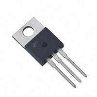
D
GD
S
G
TO-220
S
MOSFET Maximum Ratings TC = 25°C unless otherwise noted
Symbol
VDSS
VGS
Drain to Source Voltage
FDP2572
150
Unit
V
Gate to Source Voltage
±20
V
29
A
Parameter
Drain Current
Continuous (TC = 25oC, VGS = 10V)
ID
Continuous (TC = 100oC, VGS = 10V)
Continuous (Tamb = 25oC, VGS = 10V, R θJA = 43oC/W)
Pulsed
EAS
PD
TJ, TSTG
20
A
4
A
Figure 4
A
Single Pulse Avalanche Energy (Note 1)
36
mJ
Power dissipation
135
W
Derate above 25oC
0.9
W/oC
-55 to 175
oC
Operating and Storage Temperature
Thermal Characteristics
RθJC
Thermal Resistance, Junction to Case, Max.
1.11
o
C/W
RθJA
Thermal Resistance, Junction to Ambient, Max. (Note 2)
62.5
o
C/W
©2002 Fairchild Semiconductor Corporation
FDP2572 Rev. C1
1
www.fairchildsemi.com
FDP2572 — N-Channel PowerTrench® MOSFET
October 2013
�Device Marking
Device
Package
Reel Size
Tape Width
Quantity
FDP2572
FDP2572
TO-220
Tube
N/A
50 units
Electrical Characteristics TC = 25°C unless otherwise noted
Sym
Sy
mbol
Parrameter
Pa
Test Cond
Condit
itio
ions
ns
Min
Typ
Max
Unit
V
Off Characteristics
BVDSS
Drain to Source Breakdown Voltage
IDSS
Zero Gate Voltage Drain Current
IGSS
Gate to Source Leakage Current
ID = 250µA, VGS = 0V
150
-
-
-
-
1
-
-
250
VGS = ±20V
-
-
±100
nA
VGS = VDS, ID = 250µA
2
-
4
V
-
0.045
0.054
ID = 4A, VGS = 6V,
-
0.050
0.075
-
0.126
0.146
-
1770
-
-
183
-
pF
-
40
-
pF
VDS = 120V
VGS = 0V
TC = 150o
µA
On Characteristics
VGS(TH)
Gate to Source Threshold Voltage
rDS(ON)
Drain to Source On Resistance
ID = 9A,V GS = 10V
ID=9A, VGS=10V, TC=175oC
Ω
Dynamic Characteristics
CISS
Input Capacitance
COSS
Output Capacitance
CRSS
Reverse Transfer Capacitance
Qg(TOT)
Total Gate Charge at 10V
VGS = 0V to 10V
Qg(TH)
Threshold Gate Charge
VGS = 0V to 2V
Qgs
Gate to Source Gate Charge
Qgs2
Gate Charge Threshold to Plateau
Qgd
Gate to Drain “Miller” Charge
VDS = 25V, VGS = 0V,
f = 1MHz
VDD = 75V
ID = 9A
Ig = 1.0mA
pF
-
26
34
nC
-
3.3
4.3
nC
-
8
-
nC
-
5
-
nC
-
6
-
nC
ns
Resistive Switching Characteristics (VGS = 10V)
tON
Turn-On Time
-
-
36
td(ON)
Turn-On Delay Time
-
11
-
ns
tr
Rise Time
-
14
-
ns
td(OFF)
Turn-Off Delay Time
-
31
-
ns
tf
Fall Time
-
14
-
ns
tOFF
Turn-Off Time
-
-
66
ns
ISD = 9A
V
ISD = 9A, dISD/dt =100A/µs
VDD = 75V, ID = 9A
V GS = 10V, RGS = 11.0Ω
Drain-Source Diode Characteristics
VSD
Source to Drain Diode Voltage
trr
Reverse Recovery Time
QRR
Reverse Recovered Charge
-
-
1.25
ISD = 4A
-
-
1.0
V
-
-
74
ns
ISD = 9A, dISD/dt =100A/µs
-
-
169
nC
Notes:
1: Starting TJ = 25°C, L = 0.2mH, IAS = 19A.
2: Pulse Width = 100s
©2002 Fairchild Semiconductor Corporation
FDP2572 Rev. C1
2
www.fairchildsemi.com
FDP2572 — N-Channel PowerTrench® MOSFET
Package Marking and Ordering Information
�40
VGS = 10V
35
1.0
ID, DRAIN CURRENT (A)
POWER DISSIPATION MULTIPLIER
1.2
0.8
0.6
0.4
30
25
20
15
10
0.2
5
0
0
25
50
75
100
150
125
0
175
25
TC , CASE TEMPERATURE (oC)
Figure 1. Normalized Power Dissipation vs
Ambient Temperature
50
75
100
125
TC, CASE TEMPERATURE (oC)
150
175
Figure 2. Maximum Continuous Drain Current vs
Case Temperature
2.0
DUTY CYCLE - DESCENDING ORDER
0.5
0.2
0.1
0.05
0.02
0.01
ZθJC, NORMALIZED
THERMAL IMPEDANCE
1.0
PDM
0.1
SINGLE PULSE
t1
t2
NOTES:
DUTY FACTOR: D = t1/t2
PEAK TJ = PDM x ZθJC x RθJC + TC
0.01
10-5
10-4
10-3
10-2
10-1
t , RECTANGULAR PULSE DURATION (s)
100
101
Figure 3. Normalized Maximum Transient Thermal Impedance
500
TC = 25oC
FOR TEMPERATURES
ABOVE 25oC DERATE PEAK
CURRENT AS FOLLOWS:
IDM, PEAK CURRENT (A)
TRANSCONDUCTANCE
MAY LIMIT CURRENT
IN THIS REGION
175 - TC
I = I25
150
100
VGS = 10V
20
10-5
10-4
10-3
10-2
t , PULSE WIDTH (s)
10-1
100
101
Figure 4. Peak Current Capability
©2002 Fairchild Semiconductor Corporation
FDP2572 Rev. C1
3
www.fairchildsemi.com
FDP2572 — N-Channel PowerTrench® MOSFET
Typical Characteristics TC = 25°C unless otherwise noted
�1000
100
STARTING TJ = 25oC
100
IAS, AVALANCHE CURRENT (A)
ID, DRAIN CURRENT (A)
10µs
100µs
1ms
10
OPERATION IN THIS
AREA MAY BE
LIMITED BY rDS(ON)
10ms
1
SINGLE PULSE
TJ = MAX RATED
TC = 25oC
DC
STARTING TJ = 150oC
1
If R = 0
tAV = (L)(IAS)/(1.3*RATED BVDSS - VDD)
If R ≠ 0
tAV = (L/R)ln[(IAS*R)/(1.3*RATED BVDSS - VDD) +1]
0.1
0.1
1
10
100
VDS, DRAIN TO SOURCE VOLTAGE (V)
0.001
200
1
Figure 6. Unclamped Inductive Switching
Capability
60
60
PULSE DURATION = 80µs
DUTY CYCLE = 0.5% MAX
VDD = 15V
TC = 25oC
40
TJ = 175o C
30
TJ = 25o C
20
VGS = 10V
50
ID, DRAIN CURRENT (A)
50
TJ = -55oC
10
40
VGS = 7V
VGS = 6V
30
VGS = 5V
20
10
0
PULSE DURATION = 80µs
DUTY CYCLE = 0.5% MAX
0
3.0
3.5
4.0
4.5
5.0
5.5
6.0
VGS , GATE TO SOURCE VOLTAGE (V)
0
6.5
Figure 7. Transfer Characteristics
1
2
3
VDS , DRAIN TO SOURCE VOLTAGE (V)
Figure 8. Saturation Characteristics
3.0
60
PULSE DURATION = 80µs
DUTY CYCLE = 0.5% MAX
PULSE DURATION = 80µs
DUTY CYCLE = 0.5% MAX
NORMALIZED DRAIN TO SOURCE
ON RESISTANCE
DRAIN TO SOURCE ON RESISTANCE (m Ω)
0.01
0.1
tAV, TIME IN AVALANCHE (ms)
NOTE: Refer to Fairchild Application Notes AN7514 and AN7515
Figure 5. Forward Bias Safe Operating Area
ID , DRAIN CURRENT (A)
10
VGS = 6V
55
50
VGS = 10V
45
40
2.5
2.0
1.5
1.0
0.5
VGS = 10V, ID =9A
0
0
10
20
30
-80
ID, DRAIN CURRENT (A)
Figure 9. Drain to Source On Resistance vs Drain
Current
©2002 Fairchild Semiconductor Corporation
FDP2572 Rev. C1
-40
0
40
80
120
160
TJ, JUNCTION TEMPERATURE (oC)
200
Figure 10. Normalized Drain to Source On
Resistance vs Junction Temperature
4
www.fairchildsemi.com
FDP2572 — N-Channel PowerTrench® MOSFET
Typical Characteristics TC = 25°C unless otherwise noted
�1.2
1.4
ID = 250µA
NORMALIZED DRAIN TO SOURCE
BREAKDOWN VOLTAGE
VGS = VDS, ID = 250µA
NORMALIZED GATE
THRESHOLD VOLTAGE
1.2
1.0
0.8
0.6
0.4
1.1
1.0
0.9
-80
-40
0
40
80
120
160
TJ, JUNCTION TEMPERATURE (oC)
200
-80
Figure 11. Normalized Gate Threshold Voltage vs
Junction Temperature
-40
0
40
80
120
160
TJ , JUNCTION TEMPERATURE (oC)
200
Figure 12. Normalized Drain to Source
Breakdown Voltage vs Junction Temperature
1000
10
CISS = CGS + CGD
1000
C, CAPACITANCE (pF)
VGS , GATE TO SOURCE VOLTAGE (V)
VDD = 75V
COSS ≅ CDS + C GD
CRSS = CGD
100
VGS = 0V, f = 1MHz
10
8
6
4
WAVEFORMS IN
DESCENDING ORDER:
ID = 9A
ID = 4A
2
0
0.1
1
10
VDS , DRAIN TO SOURCE VOLTAGE (V)
150
0
Figure 13. Capacitance vs Drain to Source
Voltage
©2002 Fairchild Semiconductor Corporation
FDP2572 Rev. C1
5
10
15
20
Qg , GATE CHARGE (nC)
25
30
Figure 14. Gate Charge Waveforms for Constant
Gate Currents
5
www.fairchildsemi.com
FDP2572 — N-Channel PowerTrench® MOSFET
Typical Characteristics TC = 25°C unless otherwise noted
�VDS
BVDSS
tP
L
VARY tP TO OBTAIN
REQUIRED PEAK IAS
+
RG
-
VGS
VDS
IAS
VDD
VDD
DUT
tP
0V
IAS
0
0.01Ω
tAV
Figure 15. Unclamped Energy Test Circuit
Figure 16. Unclamped Energy Waveforms
VDS
VDD
Qg(TOT)
VDS
L
VGS
+
-
VGS
VGS = 10V
Qgs2
VDD
DUT
VGS = 2V
Ig(REF)
0
Qg(TH)
Qgs
Qgd
Ig(REF)
0
Figure 17. Gate Charge Test Circuit
Figure 18. Gate Charge Waveforms
VDS
tON
tOFF
td(ON)
td(OFF)
RL
tr
VDS
90%
-
VDD
10%
0
10%
DUT
90%
VGS
VGS
0
Figure 19. Switching Time Test Circuit
©2002 Fairchild Semiconductor Corporation
FDP2572 Rev. C1
90%
+
VGS
RGS
tf
50%
10%
PULSE WIDTH
50%
Figure 20. Switching Time Waveforms
6
www.fairchildsemi.com
FDP2572 — N-Channel PowerTrench® MOSFET
Test Circuits and Waveforms
�rev April 2002
LDRAIN
DPLCAP
10
Dbody 7 5 DbodyMOD
Dbreak 5 11 DbreakMOD
Dplcap 10 5 DplcapMOD
RLDRAIN
RSLC1
51
RSLC2
5
51
Ebreak 11 7 17 18 160
Eds 14 8 5 8 1
Egs 13 8 6 8 1
Esg 6 10 6 8 1
Evthres 6 21 19 8 1
Evtemp 20 6 18 22 1
EVTHRES
+ 19 8
+
LGATE
GATE
1
Lgate 1 9 9.56e-9
Ldrain 2 5 1.0e-9
Lsource 3 7 7.71e-9
11
+
17
EBREAK 18
-
50
RDRAIN
6
8
ESG
DBREAK
ESLC
-
It 8 17 1
DRAIN
2
5
+
.SUBCKT FDB2572 2 1 3 ;
CA 12 8 5.5e-10
Cb 15 14 7.4e-10
Cin 6 8 1.7e-9
EVTEMP
RGATE +
18 22
9
20
21
16
DBODY
MWEAK
6
MMED
MSTRO
RLGATE
LSOURCE
CIN
8
7
RSOURCE
RLgate 1 9 95.6
RLdrain 2 5 10
RLsource 3 7 77.1
Mmed 16 6 8 8 MmedMOD
Mstro 16 6 8 8 MstroMOD
Mweak 16 21 8 8 MweakMOD
S1A
12
S2A
13
8
S1B
CA
Rbreak 17 18 RbreakMOD 1
Rdrain 50 16 RdrainMOD 35e-3
Rgate 9 20 1.6
RSLC1 5 51 RSLCMOD 1.0e-6
RSLC2 5 50 1.0e3
Rsource 8 7 RsourceMOD 3.0e-3
Rvthres 22 8 RvthresMOD 1
Rvtemp 18 19 RvtempMOD 1
S1a 6 12 13 8 S1AMOD
S1b 13 12 13 8 S1BMOD
S2a 6 15 14 13 S2AMOD
S2b 13 15 14 13 S2BMOD
17
18
RVTEMP
S2B
13
CB
6
8
5
8
EDS
-
19
VBAT
+
IT
14
+
+
EGS
RLSOURCE
RBREAK
15
14
13
SOURCE
3
-
8
22
RVTHRES
Vbat 22 19 DC 1
ESLC 51 50 VALUE={(V(5,51)/ABS(V(5,51)))*(PWR(V(5,51)/(1e-6*52),3))}
.MODEL DbodyMOD D (IS=6.0E-11 N=1.14 RS=3.9e-3 TRS1=3.5e-3 TRS2=3.0e-6
+ CJO=1.1e-9 M=0.63 TT=6.2e-8 XTI=4.5)
.MODEL DbreakMOD D (RS=10 TRS1=5.0e-3 TRS2=-5.0e-6)
.MODEL DplcapMOD D (CJO=3.5e-10 IS=1.0e-30 N=10 M=0.65)
.MODEL MmedMOD NMOS (VTO=3.55 KP=3 IS=1e-40 N=10 TOX=1 L=1u W=1u RG=1.6)
.MODEL MstroMOD NMOS (VTO=4.0 KP=25 IS=1e-30 N=10 TOX=1 L=1u W=1u)
.MODEL MweakMOD NMOS (VTO=2.95 KP=0.05 IS=1e-30 N=10 TOX=1 L=1u W=1u RG=16 RS=0.1)
.MODEL RbreakMOD RES (TC1=1.15e-3 TC2=-9.5e-7)
.MODEL RdrainMOD RES (TC1=9.0e-3 TC2=2.5e-5)
.MODEL RSLCMOD RES (TC1=3.0e-3 TC2=2.5e-6)
.MODEL RsourceMOD RES (TC1=4.0e-3 TC2=1.0e-6)
.MODEL RvthresMOD RES (TC1=-4.1e-3 TC2=-1.0e-5)
.MODEL RvtempMOD RES (TC1=-4.0e-3 TC2=1.0e-6)
.MODEL S1AMOD VSWITCH (RON=1e-5 ROFF=0.1 VON=-5.0 VOFF=-3.5)
.MODEL S1BMOD VSWITCH (RON=1e-5 ROFF=0.1 VON=-3.5 VOFF=-5.0)
.MODEL S2AMOD VSWITCH (RON=1e-5 ROFF=0.1 VON=-0.5 VOFF=0.3)
.MODEL S2BMOD VSWITCH (RON=1e-5 ROFF=0.1 VON=0.3 VOFF=-0.5)
.ENDS
Note: For further discussion of the PSPICE model, consult A New PSPICE Sub-Circuit for the Power MOSFET Featuring Global
Temperature Options; IEEE Power Electronics Specialist Conference Records, 1991, written by William J. Hepp and C. Frank
Wheatley.
©2002 Fairchild Semiconductor Corporation
FDP2572 Rev. C1
7
www.fairchildsemi.com
FDP2572 — N-Channel PowerTrench® MOSFET
PSPICE Electrical Model
�REV April 2002
ttemplate FDB2572 n2,n1,n3
electrical n2,n1,n3
{
var i iscl
dp..model dbodymod = (isl=6.0e-11,nl=1.14,rs=3.9e-3,trs1=3.5e-3,trs2=3.0e-6,cjo=1.1e-9,m=0.63,tt=6.2e-8,xti=4.5)
dp..model dbreakmod = (rs=10,trs1=5.0e-3,trs2=-5.0e-6)
dp..model dplcapmod = (cjo=3.5e-10,isl=10.0e-30,nl=10,m=0.65)
m..model mmedmod = (type=_n,vto=3.55,kp=3,is=1e-40, tox=1)
m..model mstrongmod = (type=_n,vto=4.0,kp=25,is=1e-30, tox=1)
m..model mweakmod = (type=_n,vto=2.95,kp=0.05,is=1e-30, tox=1,rs=0.1)
LDRAIN
DPLCAP 5
DRAIN
sw_vcsp..model s1amod = (ron=1e-5,roff=0.1,von=-5.0,voff=-3.5)
2
sw_vcsp..model s1bmod = (ron=1e-5,roff=0.1,von=-3.5,voff=-5.0) 10
sw_vcsp..model s2amod = (ron=1e-5,roff=0.1,von=-0.5,voff=0.3)
RLDRAIN
RSLC1
sw_vcsp..model s2bmod = (ron=1e-5,roff=0.1,von=0.3,voff=-0.5)
51
c.ca n12 n8 = 5.5e-10
RSLC2
c.cb n15 n14 = 7.4e-10
ISCL
c.cin n6 n8 = 1.7e-9
spe.ebreak n11 n7 n17 n18 = 160 GATE
1
spe.eds n14 n8 n5 n8 = 1
spe.egs n13 n8 n6 n8 = 1
spe.esg n6 n10 n6 n8 = 1
spe.evthres n6 n21 n19 n8 = 1
spe.evtemp n20 n6 n18 n22 = 1
RDRAIN
6
8
ESG
EVTHRES
+ 19 8
+
LGATE
EVTEMP
RGATE + 18 22
9
20
21
11
DBODY
16
MWEAK
6
EBREAK
+
17
18
-
MMED
MSTRO
RLGATE
CIN
8
LSOURCE
7
SOURCE
3
RSOURCE
RLSOURCE
i.it n8 n17 = 1
S1A
12
l.lgate n1 n9 = 9.56e-9
l.ldrain n2 n5 = 1.0e-9
l.lsource n3 n7 = 7.71e-9
DBREAK
50
-
dp.dbody n7 n5 = model=dbodymod
dp.dbreak n5 n11 = model=dbreakmod
dp.dplcap n10 n5 = model=dplcapmod
S2A
13
8
res.rlgate n1 n9 = 95.6
res.rldrain n2 n5 = 10
res.rlsource n3 n7 = 77.1
15
14
13
S1B
CA
RBREAK
17
18
RVTEMP
S2B
13
CB
+
6
8
EGS
-
19
IT
14
+
VBAT
5
8
EDS
-
m.mmed n16 n6 n8 n8 = model=mmedmod, l=1u, w=1u
m.mstrong n16 n6 n8 n8 = model=mstrongmod, l=1u, w=1u
m.mweak n16 n21 n8 n8 = model=mweakmod, l=1u, w=1u
+
8
22
RVTHRES
res.rbreak n17 n18 = 1, tc1=1.15e-3,tc2=-9.5e-7
res.rdrain n50 n16 = 35e-3, tc1=9.0e-3,tc2=2.5e-5
res.rgate n9 n20 = 1.6
res.rslc1 n5 n51 = 1.0e-6, tc1=3.0e-3,tc2=2.5e-6
res.rslc2 n5 n50 = 1.0e3
res.rsource n8 n7 = 3.0e-3, tc1=4.0e-3,tc2=1.0e-6
res.rvthres n22 n8 = 1, tc1=-4.1e-3,tc2=-1.0e-5
res.rvtemp n18 n19 = 1, tc1=-4.0e-3,tc2=1.0e-6
sw_vcsp.s1a n6 n12 n13 n8 = model=s1amod
sw_vcsp.s1b n13 n12 n13 n8 = model=s1bmod
sw_vcsp.s2a n6 n15 n14 n13 = model=s2amod
sw_vcsp.s2b n13 n15 n14 n13 = model=s2bmod
v.vbat n22 n19 = dc=1
equations {
i (n51->n50) +=iscl
iscl: v(n51,n50) = ((v(n5,n51)/(1e-9+abs(v(n5,n51))))*((abs(v(n5,n51)*1e6/52))** 3))}
}
©2002 Fairchild Semiconductor Corporation
FDP2572 Rev. C1
8
www.fairchildsemi.com
FDP2572 — N-Channel PowerTrench® MOSFET
SABER Electrical Model
�th
REV 26 April 2002
JUNCTION
FDB2572
CTHERM1 TH 6 3.8e-3
CTHERM2 6 5 4.0e-3
CTHERM3 5 4 4.2e-3
CTHERM4 4 3 4.3e-3
CTHERM5 3 2 8.5e-3
CTHERM6 2 TL 3.0e-2
RTHERM1
CTHERM1
6
RTHERM1 TH 6 5.5e-4
RTHERM2 6 5 5.0e-3
RTHERM3 5 4 4.5e-2
RTHERM4 4 3 10.5e-2
RTHERM5 3 2 3.7e-1
RTHERM6 2 TL 3.8e-1
RTHERM2
CTHERM2
5
SABER Thermal Model
SABER thermal model FDB2572
template thermal_model th tl
thermal_c th, tl
{
ctherm.ctherm1 th 6 =3.8e-3
ctherm.ctherm2 6 5 =4.0e-3
ctherm.ctherm3 5 4 =4.2e-3
ctherm.ctherm4 4 3 =4.3e-3
ctherm.ctherm5 3 2 =8.5e-3
ctherm.ctherm6 2 tl =3.0e-2
RTHERM3
CTHERM3
4
RTHERM4
rtherm.rtherm1 th 6 =5.5e-4
rtherm.rtherm2 6 5 =5.0e-3
rtherm.rtherm3 5 4 =4.5e-2
rtherm.rtherm4 4 3 =10.5e-2
rtherm.rtherm5 3 2 =3.7e-1
rtherm.rtherm6 2 tl =3.8e-1
}
CTHERM4
3
RTHERM5
CTHERM5
2
RTHERM6
CTHERM6
tl
©2002 Fairchild Semiconductor Corporation
FDP2572 Rev. C1
9
CASE
www.fairchildsemi.com
FDP2572 — N-Channel PowerTrench® MOSFET
SPICE Thermal Model
�FDP2572 — N-Channel PowerTrench® MOSFET
Mechanical Dimensions
TO-220 3L
Figure 21. TO-220, Molded, 3Lead, Jedec Variation AB
Package drawings are provided as a service to customers considering Fairchild components. Drawings may change in any manner
without notice. Please note the revision and/or date on the drawing and contact a Fairchild Semiconductor representative to verify or
obtain the most recent revision. Package specifications do not expand the terms of Fairchild’s worldwide terms and conditions, specifically the warranty therein, which covers Fairchild products.
Always visit Fairchild Semiconductor’s online packaging area for the most recent package drawings:
http://www.fairchildsemi.com/package/packageDetails.html?id=PN_TT220-003
Dimension in Millimeters
©2002 Fairchild Semiconductor Corporation
FDP2572 Rev. C1
10
www.fairchildsemi.com
�tm
*Trademarks of System General Corporation, used under license by Fairchild Semiconductor.
DISCLAIMER
FAIRCHILD SEMICONDUCTOR RESERVES THE RIGHT TO MAKE CHANGES WITHOUT FURTHER NOTICE TO ANY PRODUCTS HEREIN TO IMPROVE
RELIABILITY, FUNCTION, OR DESIGN. FAIRCHILD DOES NOT ASSUME ANY LIABILITY ARISING OUT OF THE APPLICATION OR USE OF ANY
PRODUCT OR CIRCUIT DESCRIBED HEREIN; NEITHER DOES IT CONVEY ANY LICENSE UNDER ITS PATENT RIGHTS, NOR THE RIGHTS OF OTHERS.
THESE SPECIFICATIONS DO NOT EXPAND THE TERMS OF FAIRCHILD’S WORLDWIDE TERMS AND CONDITIONS, SPECIFICALLY THE WARRANTY
THEREIN, WHICH COVERS THESE PRODUCTS.
LIFE SUPPORT POLICY
FAIRCHILD’S PRODUCTS ARE NOT AUTHORIZED FOR USE AS CRITICAL COMPONENTS IN LIFE SUPPORT DEVICES OR SYSTEMS WITHOUT THE
EXPRESS WRITTEN APPROVAL OF FAIRCHILD SEMICONDUCTOR CORPORATION.
As used here in:
1. Life support devices or systems are devices or systems which, (a) are
intended for surgical implant into the body or (b) support or sustain life,
and (c) whose failure to perform when properly used in accordance with
instructions for use provided in the labeling, can be reasonably
expected to result in a significant injury of the user.
2.
A critical component in any component of a life support, device, or
system whose failure to perform can be reasonably expected to cause
the failure of the life support device or system, or to affect its safety or
effectiveness.
ANTI-COUNTERFEITING POLICY
Fairchild Semiconductor Corporation’s Anti-Counterfeiting Policy. Fairchild’s Anti-Counterfeiting Policy is also stated on our external website,
www.Fairchildsemi.com, under Sales Support.
Counterfeiting of semiconductor parts is a growing problem in the industry. All manufactures of semiconductor products are experiencing counterfeiting of their
parts. Customers who inadvertently purchase counterfeit parts experience many problems such as loss of brand reputation, substandard performance, failed
application, and increased cost of production and manufacturing delays. Fairchild is taking strong measures to protect ourselves and our customers from the
proliferation of counterfeit parts. Fairchild strongly encourages customers to purchase Fairchild parts either directly from Fairchild or from Authorized Fairchild
Distributors who are listed by country on our web page cited above. Products customers buy either from Fairchild directly or from Authorized Fairchild
Distributors are genuine parts, have full traceability, meet Fairchild’s quality standards for handing and storage and provide access to Fairchild’s full range of
up-to-date technical and product information. Fairchild and our Authorized Distributors will stand behind all warranties and will appropriately address and
warranty issues that may arise. Fairchild will not provide any warranty coverage or other assistance for parts bought from Unauthorized Sources. Fairchild is
committed to combat this global problem and encourage our customers to do their part in stopping this practice by buying direct or from authorized distributors.
PRODUCT STATUS DEFINITIONS
Definition of Terms
Datasheet Identification
Product Status
Definition
Advance Information
Formative / In Design
Datasheet contains the design specifications for product development. Specifications
may change in any manner without notice.
Preliminary
First Production
Datasheet contains preliminary data; supplementary data will be published at a later
date. Fairchild Semiconductor reserves the right to make changes at any time without
notice to improve design.
No Identification Needed
Full Production
Datasheet contains final specifications. Fairchild Semiconductor reserves the right to
make changes at any time without notice to improve the design.
Obsolete
Not In Production
Datasheet contains specifications on a product that is discontinued by Fairchild
Semiconductor. The datasheet is for reference information only.
Rev. I66
©2002 Fairchild Semiconductor Corporation
FDP2572 Rev. C1
11
www.fairchildsemi.com
FDP2572 — N-Channel PowerTrench® MOSFET
TRADEMARKS
The following includes registered and unregistered trademarks and service marks, owned by Fairchild Semiconductor and/or its global subsidiaries, and is not
intended to be an exhaustive list of all such trademarks.
Sync-Lock™
F-PFS™
AccuPower™
®
FRFET®
AX-CAP®*
®*
®
SM
BitSiC™
Global Power Resource
PowerTrench
GreenBridge™
PowerXS™
Build it Now™
TinyBoost®
Green FPS™
Programmable Active Droop™
CorePLUS™
TinyBuck®
®
Green FPS™ e-Series™
QFET
CorePOWER™
TinyCalc™
QS™
Gmax™
CROSSVOLT™
TinyLogic®
GTO™
Quiet Series™
CTL™
TINYOPTO™
IntelliMAX™
RapidConfigure™
Current Transfer Logic™
TinyPower™
ISOPLANAR™
DEUXPEED®
™
TinyPWM™
Dual Cool™
Marking Small Speakers Sound Louder
TinyWire™
EcoSPARK®
Saving our world, 1mW/W/kW at a time™
and Better™
TranSiC™
EfficentMax™
SignalWise™
MegaBuck™
TriFault Detect™
ESBC™
SmartMax™
MICROCOUPLER™
TRUECURRENT®*
SMART START™
MicroFET™
®
SerDes™
Solutions for Your Success™
MicroPak™
SPM®
MicroPak2™
Fairchild®
STEALTH™
MillerDrive™
Fairchild Semiconductor®
UHC®
SuperFET®
MotionMax™
FACT Quiet Series™
®
Ultra FRFET™
SuperSOT™-3
mWSaver
FACT®
UniFET™
SuperSOT™-6
OptoHiT™
FAST®
VCX™
SuperSOT™-8
OPTOLOGIC®
FastvCore™
VisualMax™
OPTOPLANAR®
SupreMOS®
FETBench™
VoltagePlus™
SyncFET™
FPS™
XS™
�ON Semiconductor and
are trademarks of Semiconductor Components Industries, LLC dba ON Semiconductor or its subsidiaries in the United States and/or other countries.
ON Semiconductor owns the rights to a number of patents, trademarks, copyrights, trade secrets, and other intellectual property. A listing of ON Semiconductor’s product/patent
coverage may be accessed at www.onsemi.com/site/pdf/Patent−Marking.pdf. ON Semiconductor reserves the right to make changes without further notice to any products herein.
ON Semiconductor makes no warranty, representation or guarantee regarding the suitability of its products for any particular purpose, nor does ON Semiconductor assume any liability
arising out of the application or use of any product or circuit, and specifically disclaims any and all liability, including without limitation special, consequential or incidental damages.
Buyer is responsible for its products and applications using ON Semiconductor products, including compliance with all laws, regulations and safety requirements or standards,
regardless of any support or applications information provided by ON Semiconductor. “Typical” parameters which may be provided in ON Semiconductor data sheets and/or
specifications can and do vary in different applications and actual performance may vary over time. All operating parameters, including “Typicals” must be validated for each customer
application by customer’s technical experts. ON Semiconductor does not convey any license under its patent rights nor the rights of others. ON Semiconductor products are not
designed, intended, or authorized for use as a critical component in life support systems or any FDA Class 3 medical devices or medical devices with a same or similar classification
in a foreign jurisdiction or any devices intended for implantation in the human body. Should Buyer purchase or use ON Semiconductor products for any such unintended or unauthorized
application, Buyer shall indemnify and hold ON Semiconductor and its officers, employees, subsidiaries, affiliates, and distributors harmless against all claims, costs, damages, and
expenses, and reasonable attorney fees arising out of, directly or indirectly, any claim of personal injury or death associated with such unintended or unauthorized use, even if such
claim alleges that ON Semiconductor was negligent regarding the design or manufacture of the part. ON Semiconductor is an Equal Opportunity/Affirmative Action Employer. This
literature is subject to all applicable copyright laws and is not for resale in any manner.
PUBLICATION ORDERING INFORMATION
LITERATURE FULFILLMENT:
Literature Distribution Center for ON Semiconductor
19521 E. 32nd Pkwy, Aurora, Colorado 80011 USA
Phone: 303−675−2175 or 800−344−3860 Toll Free USA/Canada
Fax: 303−675−2176 or 800−344−3867 Toll Free USA/Canada
Email: orderlit@onsemi.com
© Semiconductor Components Industries, LLC
N. American Technical Support: 800−282−9855 Toll Free
USA/Canada
Europe, Middle East and Africa Technical Support:
Phone: 421 33 790 2910
Japan Customer Focus Center
Phone: 81−3−5817−1050
www.onsemi.com
1
ON Semiconductor Website: www.onsemi.com
Order Literature: http://www.onsemi.com/orderlit
For additional information, please contact your local
Sales Representative
www.onsemi.com
�


 工商网监
湘ICP备2023018690号
工商网监
湘ICP备2023018690号
