Is Now Part of
To learn more about ON Semiconductor, please visit our website at
www.onsemi.com
Please note: As part of the Fairchild Semiconductor integration, some of the Fairchild orderable part numbers
will need to change in order to meet ON Semiconductor’s system requirements. Since the ON Semiconductor
product management systems do not have the ability to manage part nomenclature that utilizes an underscore
(_), the underscore (_) in the Fairchild part numbers will be changed to a dash (-). This document may contain
device numbers with an underscore (_). Please check the ON Semiconductor website to verify the updated
device numbers. The most current and up-to-date ordering information can be found at www.onsemi.com. Please
email any questions regarding the system integration to Fairchild_questions@onsemi.com.
ON Semiconductor and the ON Semiconductor logo are trademarks of Semiconductor Components Industries, LLC dba ON Semiconductor or its subsidiaries in the United States and/or other countries. ON Semiconductor owns the rights to a number
of patents, trademarks, copyrights, trade secrets, and other intellectual property. A listing of ON Semiconductor’s product/patent coverage may be accessed at www.onsemi.com/site/pdf/Patent-Marking.pdf. ON Semiconductor reserves the right
to make changes without further notice to any products herein. ON Semiconductor makes no warranty, representation or guarantee regarding the suitability of its products for any particular purpose, nor does ON Semiconductor assume any liability
arising out of the application or use of any product or circuit, and specifically disclaims any and all liability, including without limitation special, consequential or incidental damages. Buyer is responsible for its products and applications using ON
Semiconductor products, including compliance with all laws, regulations and safety requirements or standards, regardless of any support or applications information provided by ON Semiconductor. “Typical” parameters which may be provided in ON
Semiconductor data sheets and/or specifications can and do vary in different applications and actual performance may vary over time. All operating parameters, including “Typicals” must be validated for each customer application by customer’s
technical experts. ON Semiconductor does not convey any license under its patent rights nor the rights of others. ON Semiconductor products are not designed, intended, or authorized for use as a critical component in life support systems or any FDA
Class 3 medical devices or medical devices with a same or similar classification in a foreign jurisdiction or any devices intended for implantation in the human body. Should Buyer purchase or use ON Semiconductor products for any such unintended
or unauthorized application, Buyer shall indemnify and hold ON Semiconductor and its officers, employees, subsidiaries, affiliates, and distributors harmless against all claims, costs, damages, and expenses, and reasonable attorney fees arising out
of, directly or indirectly, any claim of personal injury or death associated with such unintended or unauthorized use, even if such claim alleges that ON Semiconductor was negligent regarding the design or manufacture of the part. ON Semiconductor
is an Equal Opportunity/Affirmative Action Employer. This literature is subject to all applicable copyright laws and is not for resale in any manner.
�FGA6530WDF
650 V, 30 A Field Stop Trench IGBT
Features
General Description
• Maximum Junction Temperature : TJ =
175oC
Using novel field stop IGBT technology, Fairchild’s new series of
field stop 3rd generation IGBTs offer the optimum performance
for welder and industial applications where low conduction and
switching losses are essential.
• Positive Temperaure Co-efficient for Easy Parallel Operating
• High Current Capability
• Low Saturation Voltage: VCE(sat) = 1.8 V(Typ.) @ IC = 30 A
• 100% of the Parts Tested for ILM(1)
Applications
• High Input Impedance
• Welder and Industrial Application
• Fast Switching
• Power Factor Correction
• Tighten Parameter Distribution
• RoHS Compliant
C
G
G
C
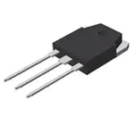
TO-3PN
E
Absolute Maximum Ratings T
C
Symbol
VCES
VGES
E
= 25°C unless otherwise noted
Description
FGA6530WDF
Unit
Collector to Emitter Voltage
650
V
Gate to Emitter Voltage
20
V
30
V
Collector Current
@ TC = 25oC
60
A
Collector Current
@ TC = 100oC
30
A
ILM (1)
Pulsed Collector Current
@ TC = 25oC
90
A
ICM (2)
Pulsed Collector Current
IC
IF
IFM
PD
Transient Gate to Emitter Voltage
90
A
Diode Forward Current
@ TC = 25oC
30
A
Diode Forward Current
o
15
A
60
A
W
@ TC = 100 C
Pulsed Diode Maximum Forward Current
o
Maximum Power Dissipation
@ TC = 25 C
176
Maximum Power Dissipation
@ TC = 100oC
88
W
TJ
Operating Junction Temperature
-55 to +175
o
Tstg
Storage Temperature Range
-55 to +175
o
C
TL
Maximum Lead Temp. for soldering
Purposes, 1/8” from case for 5 seconds
300
o
C
C
Notes:
1. VCC = 400 V, VGE = 15 V, IC = 90 A, RG = 55.9 Inductive Load
2. Repetitive rating: Pulse width limited by max. junction temperature
©2015 Fairchild Semiconductor Corporation
FGA6530WDF Rev. 1.1
1
www.fairchildsemi.com
FGA6530WDF — 650 V, 30 A Field Stop Trench IGBT
August 2015
�Symbol
Parameter
FGA6530WDF
Unit
o
RJC(IGBT)
Thermal Resistance, Junction to Case, Max.
0.85
RJC(Diode)
Thermal Resistance, Junction to Case, Max.
3.5
oC/W
C/W
RJA
Thermal Resistance, Junction to Ambient, Max.
40
oC/W
Package Marking and Ordering Information
Part Number
Top Mark
Package
Packing Method
Reel Size
Tape Width
Quantity
FGA6530WDF
FGA6530WDF
TO-3PN
Tube
-
-
30
Electrical Characteristics of the IGBT
Symbol
Parameter
TC = 25°C unless otherwise noted
Test Conditions
Min.
Typ.
Max.
Unit
650
-
-
V
-
0.52
-
V/oC
Off Characteristics
BVCES
Collector to Emitter Breakdown Voltage VGE = 0 V, IC = 1 mA
BVCES
TJ
Temperature Coefficient of Breakdown
Voltage
ICES
Collector Cut-Off Current
VCE = VCES, VGE = 0 V
-
-
250
A
IGES
G-E Leakage Current
VGE = VGES, VCE = 0 V
-
-
±400
nA
IC = 30 mA, VCE = VGE
IC = 1 mA, Reference to 25oC
On Characteristics
VGE(th)
VCE(sat)
G-E Threshold Voltage
Collector to Emitter Saturation Voltage
4.1
5.6
7.6
V
IC = 30 A, VGE = 15 V
-
1.8
2.3
V
IC = 30 A, VGE = 15 V,
TC = 175oC
-
2.4
-
V
-
1072
-
pF
VCE = 30 V, VGE = 0 V,
f = 1MHz
-
36
-
pF
-
13
-
pF
-
12
-
ns
Dynamic Characteristics
Cies
Input Capacitance
Coes
Output Capacitance
Cres
Reverse Transfer Capacitance
Switching Characteristics
td(on)
Turn-On Delay Time
tr
Rise Time
-
19.2
-
ns
td(off)
Turn-Off Delay Time
-
42.4
-
ns
tf
Fall Time
Eon
Turn-On Switching Loss
Eoff
Turn-Off Switching Loss
-
162
-
uJ
Ets
Total Switching Loss
-
1122
-
uJ
td(on)
Turn-On Delay Time
-
12.8
-
ns
tr
Rise Time
-
27.2
-
ns
td(off)
Turn-Off Delay Time
tf
Fall Time
Eon
Turn-On Switching Loss
Eoff
Turn-Off Switching Loss
Ets
Total Switching Loss
©2015 Fairchild Semiconductor Corporation
FGA6530WDF Rev. 1.1
VCC = 400 V, IC = 30 A,
RG = 6 , VGE = 15 V,
Inductive Load, TC = 25oC
VCC = 400 V, IC = 30 A,
RG = 6 , VGE = 15 V,
Inductive Load, TC = 175oC
2
-
7.2
-
ns
-
960
-
uJ
-
46.4
-
ns
-
12.8
-
ns
-
1430
-
uJ
-
310
-
uJ
-
1740
-
uJ
www.fairchildsemi.com
FGA6530WDF — 650 V, 30 A Field Stop Trench IGBT
Thermal Characteristics
�Symbol
Parameter
Qg
Total Gate Charge
Qge
Gate to Emitter Charge
Qgc
Gate to Collector Charge
Test Conditions
VCE = 400 V, IC = 30 A,
VGE = 15 V
Electrical Characteristics of the Diode
Symbol
Parameter
VFM
Diode Forward Voltage
Erec
Reverse Recovery Energy
trr
Diode Reverse Recovery Time
Qrr
Diode Reverse Recovery Charge
©2015 Fairchild Semiconductor Corporation
FGA6530WDF Rev. 1.1
(Continued)
Min.
Typ.
Max
Unit
-
37.4
-
nC
-
7.2
-
nC
-
15
-
nC
Unit
TC = 25°C unless otherwise noted
Test Conditions
IF = 15 A
IF = 15 A, dIF/dt = 200 A/s
3
Min.
Typ.
Max
TC = 25oC
-
1.7
2.6
TC = 175oC
-
1.62
-
TC = 175oC
-
76
-
TC =
25oC
-
81
-
TC = 175oC
-
257
-
TC = 25oC
-
254
-
TC = 175oC
-
1189
-
V
uJ
ns
nC
www.fairchildsemi.com
FGA6530WDF — 650 V, 30 A Field Stop Trench IGBT
Electrical Characteristics of the IGBT
�Figure 1. Typical Output Characteristics
90
10V
60
45
VGE = 8V
45
0
1
2
3
4
5
Collector-Emitter Voltage, VCE [V]
0
6
Common Emitter
VGE = 15V
o
TC = 25 C
o
TC = 175 C
60
45
30
15
0
1
2
3
4
Collector-Emitter Voltage, VCE [V]
5
Common Emitter
VGE = 15V
3
60A
30A
2
IC = 15A
Figure 6. Saturation Voltage vs. VGE
20
Common Emitter
Common Emitter
o
o
Collector-Emitter Voltage, VCE [V]
TC = 25 C
16
12
IC = 15A
8
30A
60A
4
4
8
12
16
Gate-Emitter Voltage, VGE [V]
©2015 Fairchild Semiconductor Corporation
FGA6530WDF Rev. 1.1
6
1
-100
-50
0
50
100
150
200
o
Collector-Emitter Case Temperature, TC [ C]
Figure 5. Saturation Voltage vs. VGE
20
1
2
3
4
5
Collector-Emitter Voltage, VCE [V]
Figure 4. Saturation Voltage vs. Case
Temperature at Variant Current Level
Collector-Emitter Voltage, VCE [V]
Collector Current, IC [A]
0
4
75
Collector-Emitter Voltage, VCE [V]
VGE = 8V
30
90
0
10V
15
Figure 3. Typical Saturation Voltage
Characteristics
0
12V
60
15
0
15V
75
12V
30
20V
o
TC = 175 C
15V
Collector Current, IC [A]
Collector Current, IC [A]
90
20V
o
TC = 25 C
75
Figure 2. Typical Output Characteristics
TC = 175 C
16
12
30A
8
IC = 15A
4
0
20
4
60A
4
8
12
16
Gate-Emitter Voltage, VGE [V]
20
www.fairchildsemi.com
FGA6530WDF — 650 V, 30 A Field Stop Trench IGBT
Typical Performance Characteristics
�Figure 7. Capacitance Characteristics
Figure 8. Gate charge Characteristics
15
10000
Common Emitter
Gate-Emitter Voltage, VGE [V]
Capacitance [pF]
o
Cies
1000
100
Coes
Common Emitter
VGE = 0V, f = 1MHz
o
300V
9
10
Collector-Emitter Voltage, VCE [V]
3
30
Figure 9. Turn-on Characteristics vs.
Gate Resistance
0
8
16
24
Gate Charge, Qg [nC]
40
1000
td(on)
10
Switching Time [ns]
tr
Switching Time [ns]
32
Figure 10. Turn-off Characteristics vs.
Gate Resistance
100
Common Emitter
VCC = 400V, VGE = 15V
IC = 30A
td(off)
100
tf
Common Emitter
VCC = 400V, VGE = 15V
IC = 30A
10
o
TC = 25 C
o
TC = 25 C
o
TC = 175 C
o
TC = 175 C
5
400V
6
0
1
VCC = 200V
Cres
TC = 25 C
10
TC = 25 C
12
1
0
10
20
30
40
50
60
Gate Resistance, RG []
70
80
Figure 11. Switching Loss vs.
Gate Resistance
0
10
20
30
40
50
60
Gate Resistance, RG []
70
80
Figure 12. Turn-on Characteristics vs.
Collector Current
300
5000
Switching Time [ns]
Switching Loss [uJ]
100
Eon
1000
Eoff
Common Emitter
VCC = 400V, VGE = 15V
IC = 30A
10
td(on)
Common Emitter
VGE = 15V, RG = 6
o
o
TC = 25 C
TC = 25 C
100
o
o
TC = 175 C
TC = 175 C
50
tr
0
10
20
30
40
50
60
Gate Resistance, RG []
©2015 Fairchild Semiconductor Corporation
FGA6530WDF Rev. 1.1
1
70
80
0
15
30
45
60
75
90
Collector Current, IC [A]
5
www.fairchildsemi.com
FGA6530WDF — 650 V, 30 A Field Stop Trench IGBT
Typical Performance Characteristics
�Figure 13. Turn-off Characteristics vs.
Collector Current
Figure 14. Switching Loss vs.
Collector Current
10000
300
Eon
100
10
Switching Loss [uJ]
Switching Time [ns]
td(off)
tf
Common Emitter
VGE = 15V, RG = 6
1000
Eoff
100
Common Emitter
VGE = 15V, RG = 6
o
TC = 25 C
o
TC = 25 C
o
TC = 175 C
o
1
TC = 175 C
0
15
30
45
60
Collector Current, IC [A]
10
75
90
0
15
30
45
60
75
90
Collector Current, IC [A]
Figure 15. Load Current Vs. Frequency
Figure 16. SOA Characteristics
100
150
Square Wave
o
10s
VGE = 15/0V, RG = 6
Collector Current, Ic [A]
Collector Current, [A]
TJ


 工商网监
湘ICP备2023018690号
工商网监
湘ICP备2023018690号
