LMV981, LMV982
Single and Dual Low
Voltage, Rail-to-Rail Input
and Output, Operational
Amplifiers with Shutdown
The LMV981 Single and LMV982 Dual are low−voltage
operational amplifiers which can operate on single−sided power
supplies (1.8 V to 5.0 V) with rail−to−rail input and output swing.
Both devices come in small state−of−the−art packages and require
very low quiescent current making them ideal for battery−operated,
portable applications such as notebook computers and hand−held
instruments. Rail−to−Rail operation allows for optimal
signal−to−noise applications plus the small packages allow for closer
placement to signal sources further enhancing overall signal chain
performance.
The LMV981 Single and LMV982 Dual both have a shutdown pin
that can be used to disable the device and further reduce power
consumption. Shutdown is implemented by driving the SHDN Pin LOW.
Features
• Specified at Single−Sided Power Supply: 1.8 V, 2.7 V, and 5 V
• Small Packages:
•
•
•
•
•
LMV981 in a SC−70* and uLLGA (1.5mm x 1.5mm x 0.4mm)
LMV982 in a Micro10* and uQFN (1.4mm x 1.8mm x 0.6 mm)
No Output Crossover Distortion
Extended Industrial Temperature Range: −40°C to +125°C
Low Quiescent Current 210 mA, max per channel
No Output Phase−Reversal from Overdriven Input
These are Pb−Free Devices
www.onsemi.com
MARKING
DIAGRAMS
LMV981 (Single)
6
1
SC−70*
CASE 419B
AAE MG
G
1
1
V MG
G
1
ULLGA8
CASE 613AG
M = Date Code
G
= Pb−Free Package
(Note: Microdot may be in either location)
LMV982 (Dual)
V982
AYW
Micro10*
CASE 846B
Typical Applications
• Notebook Computers, Portable Battery−Operated Instruments, PDA’s
• Active Filters, Supply−Current Monitoring
0.1
1
UQFN10
CASE 488AT
RL = 600 W
TA = 25°C
0.09
DE MG
G
DV FROM RAIL (V)
0.08
A
= Assembly Location
Y
= Year
W = Work Week
G
= Pb−Free Package
(Note: Microdot may be in either location)
0.07
0.06
0.05
0.04
VOH
0.03
0.02
0
1.8
ORDERING INFORMATION
VOL
0.01
2.2
2.6
3
3.4
3.8
SUPPLY VOLTAGE (V)
See detailed ordering and shipping information in the package
dimensions section on page 17 of this data sheet.
4.2
4.6
5
Figure 1. Output Voltage Swing vs. Supply Voltage
© Semiconductor Components Industries, LLC, 2015
October, 2015 − Rev. 12
1
*Consult sales for package availability
Publication Order Number:
LMV981/D
�LMV981, LMV982
PIN CONNECTIONS
SC70−6*
1
NC
VCC
+IN
2
IN−
5
+
−
VEE
3
Micro10*
ULLGA8/QFN
6
SHDN
IN+
1
2
4
−IN
OUT
VEE
8
7
−
+
3
IN A−
2
IN A+
3
VEE
4
7 IN B+
5
6 SHDN B
10 VCC
A
− +
SHDN
9 OUT B
B
+ −
8 IN B−
VCC
5
VEE
(Top View)
1
OUT
6
4
OUT A
NC − No internal connection
(Top View)
SHDN A
UQFN10
7
SHDN A
8
SHDN B
9
+INB
10
(Top View)
+INA
VEE
6
−INA
4
OUTA
3
VCC
−
+
+
−
1
5
2
−INB
OUTB
(Top View)
*Consult sales for package availability
MAXIMUM RATINGS
Symbol
VS
Rating
Supply Voltage (Operating Range VS = 2.7 V to 5.5 V)
Value
Unit
5.5
V
VIDR
Input Differential Voltage
$Supply Voltage
V
VICR
Input Common Mode Voltage Range
−0.5 to (V+) + 0.5
V
10
mA
Maximum Input Current
tSo
Output Short Circuit (Note 1)
TJ
Maximum Junction Temperature (Operating Range −40°C to 85°C)
Continuous
150
°C
qJA
Thermal Resistance
280
340
200
300
°C/W
Tstg
Storage Temperature (SOT23−6)
−65 to 150
°C
260
°C
SC−70
ULLGA8
Micro10
UQFN10
Mounting Temperature (Infrared or Convection −30 sec)
Stresses exceeding those listed in the Maximum Ratings table may damage the device. If any of these limits are exceeded, device
functionality should not be assumed, damage may occur and reliability may be affected.
ESD data available upon request.
1. Continuous short−circuit operation to ground at elevated ambient temperature can result in exceeding the maximum allowed junction
temperature of 150°C. Output currents in excess of 45 mA over long term may adversely affect reliability. Shorting output to either V+
or V− will adversely affect reliability.
www.onsemi.com
2
�LMV981, LMV982
1.8 V DC ELECTRICAL CHARACTERISTICS Unless otherwise noted, all min/max limits are guaranteed for TA = 25°C,
V+ = 1.8 V, V− = 0 V, VCM = V+/2, VO = V+/2 and RL > 1 MW. Typical specifications represent the most likely parametric norm.
Parameter
Input Offset Voltage
Input Offset Voltage
Average Drift
Symbol
Condition
VIO
Min
Typ
Max
Unit
LMV981 (Single) (−40°C to +125°C)
1
6
mV
LMV982 (Dual) (−40°C to +125°C)
1
7.5
TCVIO
5.5
mV/°C
Input Bias Current
(Note 2)
IB
−40°C to +125°C
1 MW. Typical specifications represent the most likely parametric norm. Min/Max
specifications are guaranteed by testing, characterization, or statistical analysis.
Parameter
Slew Rate
Symbol
Condition
SR
(Note 3)
Min
Typ
Max
Unit
0.35
V/mS
GBWP
1.4
MHz
Phase Margin
Qm
67
°
Gain Margin
Gm
7
dB
Input−Referred
Voltage Noise
en
f = 50 kHz, VCM = 0.5 V
60
nV/√Hz
Total Harmonic
Distortion
THD
f = 1 kHz, AV = +1, RL = 600 W, VO = 1 VPP
0.023
%
(Note 4)
123
dB
Gain Bandwidth
Product
Amplifier−to−Amplifier
Isolation
3. Connected as voltage follower with input step from V− to V+. Number specified is the slower of the positive and negative slew rates.
4. Input referred, RL = 100 kW connected to V+/2. Each amp excited in turn with 1 kHz to produce VO = 3 VPP. (For Supply Voltages < 3 V,
VO = V+).
www.onsemi.com
4
�LMV981, LMV982
2.7V DC ELECTRICAL CHARACTERISTICS Unless otherwise noted, all min/max limits are guaranteed for TA = 25°C,
V+ = 2.7 V, V− = 0 V, VCM = V+/2, VO = V+/2 and RL > 1 MW. Typical specifications represent the most likely parametric norm.
Parameter
Input Offset Voltage
Input Offset Voltage
Average Drift
Symbol
Condition
VIO
Min
Typ
Max
Unit
LMV981 (Single) (−40°C to +125°C)
1
6
mV
LMV982 (Dual) (−40°C to +125°C)
1
7.5
TCVIO
5.5
mV/°C
Input Bias Current
(Note 5)
IB
−40°C to +125°C
1 MW. Typical specifications represent the most likely parametric norm. Min/Max
specifications are guaranteed by testing, characterization, or statistical analysis.
Parameter
Slew Rate
Symbol
Condition
SR
(Note 6)
Min
Typ
Max
Unit
0.4
V/uS
GBWP
1.4
MHz
Phase Margin
Qm
70
°
Gain Margin
Gm
7.5
dB
Input−Referred
Voltage Noise
en
f = 50 kHz, VCM = 1.0 V
57
nV/√Hz
Total Harmonic
Distortion
THD
f = 1 kHz, AV = +1, RL = 600 W, VO = 1 VPP
0.022
%
(Note 7)
123
dB
Gain Bandwidth
Product
Amplifier−to−Amplifier
Isolation
6. Connected as voltage follower with input step from V− to V+. Number specified is the slower of the positive and negative slew rates.
7. Input referred, RL = 100 kW connected to V+/2. Each amp excited in turn with 1 kHz to produce VO = 3 VPP. (For Supply Voltages < 3 V,
VO = V+).
www.onsemi.com
6
�LMV981, LMV982
5V DC ELECTRICAL CHARACTERISTICS Unless otherwise noted, all min/max limits are guaranteed for TA = 25°C, V+ = 5 V,
V− = 0 V, VCM = V+/2, VO = V+/2 and RL > 1 MW. Typical specifications represent the most likely parametric norm.
Parameter
Input Offset Voltage
Input Offset Voltage
Average Drift
Symbol
Condition
VIO
Min
Typ
Max
Unit
LMV981 (Single) (−40°C to +125°C)
1
6
mV
LMV982 (Dual) (−40°C to +125°C)
1
7.5
TCVIO
5.5
mV/°C
Input Bias Current
(Note 8)
IB
−40°C to +125°C
1 MW. Typical specifications represent the most likely parametric norm.
Parameter
Slew Rate
Symbol
Condition
SR
(Note 9)
Min
Typ
Max
Unit
0.48
V/uS
GBWP
1.5
MHz
Phase Margin
Qm
65
°
Gain Margin
Gm
8
dB
Input−Referred
Voltage Noise
en
f = 50 kHz, VCM = 2 V
50
nV/√Hz
Total Harmonic
Distortion
THD
f = 1 kHz, AV = +1, RL = 600 W, VO = 1 VPP
0.022
%
(Note 10)
123
dB
Gain Bandwidth
Product
Amplifier−to−
Amplifier Isolation
9. Connected as voltage follower with input step from V− to V+. Number specified is the slower of the positive and negative slew rates.
10. Input referred, RL = 100 kW connected to V+/2. Each amp excited in turn with 1 kHz to produce VO = 3 VPP. (For Supply Voltages < 3 V,
VO = V+).
www.onsemi.com
8
�LMV981, LMV982
TYPICAL CHARACTERISTICS
(TA = 25°C and VS = 5 V unless otherwise specified)
100
0.12
LMV981 (Single)
OUTPUT CURRENT (mA)
SUPPLY CURRENT (mA)
VCC = 5.0 V
25°C
0.1
0.08
125°C
−40°C
0.06
0.04
0.02
0
1.8
2.2
2.6
3
3.4
3.8
4.2
4.6
10
VCC = 2.7 V
1
VCC = 1.8 V
0.1
0.01
0.001
5
0.01
0.1
1.0
OUTPUT VOLTAGE REFERENCED TO VCC (V)
Figure 2. Supply Current vs. Supply Voltage
Figure 3. Sourcing Current vs. Output Voltage
(TA = 255C)
0.1
100
RL = 600 W
TA = 25°C
0.09
VCC = 2.7 V
0.08
DV FROM RAIL (V)
VCC = 5.0 V
10
VCC = 1.8 V
1
0.1
0.07
0.06
0.05
0.04
VOH
0.03
0.02
0.01
0.01
0.001
VOL
0
0.01
0.1
1.0
1.8
10
2.2
2.6
3
3.4
3.8
4.2
4.6
OUTPUT VOLTAGE REFERENCED TO VEE (V)
SUPPLY VOLTAGE (V)
Figure 4. Sinking Current vs. Output Voltage
(TA = 255C)
Figure 5. Output Voltage Swing vs. Supply
Voltage
0.02
0.018
RL = 2.0 W
TA = 25°C
0.016
DV FROM RAIL (V)
OUTPUT CURRENT (mA)
10
SUPPLY VOLTAGE (V)
0.014
0.012
VOL
0.01
0.008
VOH
0.006
0.004
0.002
0
1.8
2.2
2.6
3
3.4
3.8
4.2
SUPPLY VOLTAGE (V)
4.6
Figure 6. Output Voltage vs. Supply Voltage
www.onsemi.com
9
5
5
�LMV981, LMV982
TYPICAL CHARACTERISTICS
(TA = 25°C and VS = 5 V unless otherwise specified)
110
60
90
50
40
70
30
50
Gain
20
10
30
10
CL = 200 pF
VS = 1.8 V
RL = 610 W
TA = 25°C
0
−10
10k
PHASE (°)
GAIN (dB)
Phase
−10
100k
1M
10M
−30
FREQUENCY (Hz)
Figure 7. Gain and Phase vs. Frequency
60
CL = 200 pF
VS = 5 V
RL = 610 W
TA = 25°C
50
Phase
90
45
30
0
20
Gain
−45
10
−90
0
−10
10k
PHASE (°)
GAIN (dB)
40
135
100k
1M
FREQUENCY (Hz)
Figure 8. Gain and Phase vs. Frequency
www.onsemi.com
10
−135
10M
�LMV981, LMV982
TYPICAL CHARACTERISTICS
(TA = 25°C and VS = 5 V unless otherwise specified)
60
110
50
90
40
70
30
50
20
10
0
30
Gain
CL = 0 pF
VS = 1.8 V
RL = 100 kW
TA = 25°C
−10
10k
PHASE (°)
GAIN (dB)
Phase
10
−10
100k
1M
FREQUENCY (Hz)
−30
10M
60
110
50
90
40
70
30
50
20
30
10
0
−10
10k
10
CL = 0 pF
VS = 5.0 V
RL = 100 kW
TA = 25°C
−10
100k
1M
FREQUENCY (Hz)
Figure 10. Gain and Phase vs. Frequency
www.onsemi.com
11
−30
10M
PHASE (°)
GAIN (dB)
Figure 9. Gain and Phase vs. Frequency
�LMV981, LMV982
TYPICAL CHARACTERISTICS
(TA = 25°C and VS = 5 V unless otherwise specified)
100
80
70
VS = 5 V
60
VS = 2.7 V
60
VS = 1.8 V
40
50
PSRR (dB)
CMRR (dB)
80
40
30
20
20
10
0
10
VS = 5 V
100
1000
0
10
10k
100
FREQUENCY (Hz)
Figure 11. CMRR vs. Frequency
10k
Figure 12. PSRR vs. Frequency
10k
10
1k
THD (%)
1
100
VS = 2.7 V
0.1
VS = 1.8 V
10
VS = 5 V
1
10
100
1k
10k
0.01
10
100k
100
FREQUENCY (Hz)
1k
Figure 14. THD vs. Frequency
0.6
Falling Edge
0.5
0.4
Rising Edge
0.3
0.2
0.1
0
1.8
10k
FREQUENCY (Hz)
Figure 13. Input Voltage Noise vs. Frequency
SLEW RATE (V/ms)
INPUT VOLTAGE NOISE (nV/√HZ)
1000
FREQUENCY (Hz)
2.2
2.6
3
3.4
3.8
4.2
4.6
SUPPLY VOLTAGE (V)
Figure 15. Slew Rate vs. Supply Voltage
www.onsemi.com
12
5
100k
�LMV981, LMV982
TYPICAL CHARACTERISTICS
(TA = 25°C and VS = 5 V unless otherwise specified)
VS = 1.8 V
RL = 2 kW
TIME (2ms/div)
Figure 16. Small Signal Noninverting Response
VS = 2.7 V
RL = 2 kW
TIME (2ms/div)
Figure 17. Small Signal Noninverting Response
www.onsemi.com
13
�LMV981, LMV982
TYPICAL CHARACTERISTICS
(TA = 25°C and VS = 5 V unless otherwise specified)
VS = 5.0 V
RL = 2 kW
TIME (2ms/div)
Figure 18. Small Signal Noninverting Response
VS = 1.8 V
RL = 2 kW
TIME (2ms/div)
Figure 19. Large Signal Noninverting Response
www.onsemi.com
14
�LMV981, LMV982
TYPICAL CHARACTERISTICS
(TA = 25°C and VS = 5 V unless otherwise specified)
VS = 2.7 V
RL = 2 kW
TIME (2ms/div)
Figure 20. Large Signal Noninverting Response
VS = 5.0 V
RL = 2 kW
TIME (2ms/div)
Figure 21. Large Signal Noninverting Response
www.onsemi.com
15
�LMV981, LMV982
TYPICAL CHARACTERISTICS
110
110
100
100
SHORT−CIRCUIT CURRENT (mA)
SHORT−CIRCUIT CURRENT (mA)
(TA = 25°C and VS = 5 V unless otherwise specified)
VCC = 2.7 V
90
VCC = 5 V
80
70
60
VCC = 1.8 V
50
40
30
20
10
0
−40
−20
0
20
40
60
80
100
90
VCC = 5 V
80
70
60
VCC = 2.7 V
50
40
30
20
VCC = 1.8 V
10
0
−40
120
−20
0
20
TEMPERATURE (°C)
40
60
80
100
120
TEMPERATURE (°C)
Figure 22. Short−Circuit vs. Supply Voltage
(Sinking)
Figure 23. Short−Circuit vs. Supply Voltage
(Sourcing)
6
7
VS = 1.8 V
VS = 2.7 V
125°C
6
5
5
VOS (mV)
3
25°C
2
−40°C
125°C
1
−40°C
4
85°C
3
2
1
25°C
0
−1
0
85°C
−2
−3
−0.5
−1
−0.5
0
0.5
1
1.5
2
2.5
0
0.5
1
VCM (V)
2
2.5
3
Figure 25. Offset Voltage vs. Common Mode
Range VDD 2.7 V
8
125°C
25°C
VS = 5.0 V
6
4
−40°C
2
85°C
0
−2
−4
−6
1.5
VCM (V)
Figure 24. Offset Voltage vs. Common Mode
Range VDD 1.8 V
VOS (mV)
VOS (mV)
4
−1
0
1
2
3
4
5
VCM (V)
Figure 26. Offset Voltage vs. Common Mode
Range VDD 5.0 V
www.onsemi.com
16
6
3.5
�LMV981, LMV982
APPLICATION INFORMATION
50 k
R1
5.0 k
VCC
VCC
R2
10 k
MC1403
VO
LMV981
VO
LMV981
VCC
−
Vref
−
+
+
fO +
1
V ref + V CC
2
2.5 V
R
R1
V O + 2.5 V(1 )
)
R2
R
Figure 27. Voltage Reference
For: fo = 1.0 kHz
R = 16 kW
C = 0.01 mF
C
C
1
2pRC
Figure 28. Wien Bridge Oscillator
VCC
C
R1
R3
C
−
Vin
R2
R1
+
R2
VOH
LMV981
VO
−
VOL
CO = 10 C
Vref
VO
+
Vin
VO
LMV981
Hysteresis
Vref
CO
VinL
Given: fo = center frequency
A(fo) = gain at center frequency
VinH
Choose value fo, C
Q
Then : R3 +
pf O C
Vref
R1
(V OL * V ref) ) V ref
R1 ) R2
R1
V inH +
(V OH * V ref) ) V ref
R1 ) R2
R1
H+
(V OH * V OL)
R1 ) R2
V inL +
R1 +
R2 +
Figure 29. Comparator with Hysteresis
R3
2 A(f O)
R1 R3
4Q 2 R1 * R3
For less than 10% error from operational amplifier,
((QO fO)/BW) < 0.1 where fo and BW are expressed in Hz.
If source impedance varies, filter may be preceded with
voltage follower buffer to stabilize filter parameters.
Figure 30. Multiple Feedback Bandpass Filter
ORDERING INFORMATION
# of Channels
Specific Device Marking
Package Type
Shipping†
LMV981SQ3T2G*
Single
AAE
SC70−6*
(Pb−Free)
3000 / Tape & Reel
LMV981MU3TBG
Single
V
ULLGA8
(Pb−Free)
3000 / Tape & Reel
LMV982DMR2G*
Dual
V982
Micro10*
(Pb−Free)
4000 / Tape & Reel
LMV982MUTAG
Dual
DE
UQFN10
(Pb−Free)
3000 / Tape & Reel
Order Number
†For information on tape and reel specifications, including part orientation and tape sizes, please refer to our Tape and Reel Packaging
Specifications Brochure, BRD8011/D.
*Consult sales for package availability.
www.onsemi.com
17
�MECHANICAL CASE OUTLINE
PACKAGE DIMENSIONS
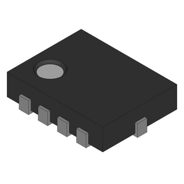
UQFN10 1.4x1.8, 0.4P
CASE 488AT−01
ISSUE A
DATE 01 AUG 2007
1
SCALE 5:1
EDGE OF PACKAGE
D
ÉÉÉ
ÉÉÉ
ÉÉÉ
PIN 1 REFERENCE
2X
2X
A
0.10 C
L1
E
0.10 C
B
TOP VIEW
A1
0.05 C
A1
C
SIDE VIEW
3
9X
EXPOSED Cu
A
0.05 C
10X
DETAIL A
Bottom View
(Optional)
5
ÉÉÉ
ÉÉÉ
SEATING
PLANE
DETAIL B
Side View
(Optional)
6
e
1
10
10 X
L3
b
A3
DIM
A
A1
A3
b
D
E
e
L
L1
L3
MILLIMETERS
MIN
MAX
0.45
0.60
0.00
0.05
0.127 REF
0.15
0.25
1.40 BSC
1.80 BSC
0.40 BSC
0.30
0.50
0.00
0.15
0.40
0.60
GENERIC
MARKING DIAGRAM*
XXMG
G
e/2
L
MOLD CMPD
NOTES:
1. DIMENSIONING AND TOLERANCING PER ASME
Y14.5M, 1994.
2. CONTROLLING DIMENSION: MILLIMETERS
3. DIMENSION b APPLIES TO PLATED TERMINAL
AND IS MEASURED BETWEEN 0.25 AND 0.30 MM
FROM TERMINAL.
4. COPLANARITY APPLIES TO THE EXPOSED PAD
AS WELL AS THE TERMINALS.
XX
= Specific Device Code
M
= Date Code
G
= Pb−Free Package
(Note: Microdot may be in either location)
0.10 C A B
0.05 C
*This information is generic. Please refer to
device data sheet for actual part marking.
Pb−Free indicator, “G” or microdot “ G”,
may or may not be present.
NOTE 3
BOTTOM VIEW
MOUNTING FOOTPRINT
1.700
0.0669
0.663
0.0261
0.200
0.0079
9X
0.563
0.0221
1
2.100
0.0827
0.400
0.0157
PITCH
DOCUMENT NUMBER:
DESCRIPTION:
10 X
0.225
0.0089
SCALE 20:1
98AON22493D
mm Ǔ
ǒinches
Electronic versions are uncontrolled except when accessed directly from the Document Repository.
Printed versions are uncontrolled except when stamped “CONTROLLED COPY” in red.
10 PIN UQFN, 1.4 X 1.8, 0.4P
PAGE 1 OF 1
ON Semiconductor and
are trademarks of Semiconductor Components Industries, LLC dba ON Semiconductor or its subsidiaries in the United States and/or other countries.
ON Semiconductor reserves the right to make changes without further notice to any products herein. ON Semiconductor makes no warranty, representation or guarantee regarding
the suitability of its products for any particular purpose, nor does ON Semiconductor assume any liability arising out of the application or use of any product or circuit, and specifically
disclaims any and all liability, including without limitation special, consequential or incidental damages. ON Semiconductor does not convey any license under its patent rights nor the
rights of others.
© Semiconductor Components Industries, LLC, 2019
www.onsemi.com
�onsemi,
, and other names, marks, and brands are registered and/or common law trademarks of Semiconductor Components Industries, LLC dba “onsemi” or its affiliates
and/or subsidiaries in the United States and/or other countries. onsemi owns the rights to a number of patents, trademarks, copyrights, trade secrets, and other intellectual property.
A listing of onsemi’s product/patent coverage may be accessed at www.onsemi.com/site/pdf/Patent−Marking.pdf. onsemi reserves the right to make changes at any time to any
products or information herein, without notice. The information herein is provided “as−is” and onsemi makes no warranty, representation or guarantee regarding the accuracy of the
information, product features, availability, functionality, or suitability of its products for any particular purpose, nor does onsemi assume any liability arising out of the application or use
of any product or circuit, and specifically disclaims any and all liability, including without limitation special, consequential or incidental damages. Buyer is responsible for its products
and applications using onsemi products, including compliance with all laws, regulations and safety requirements or standards, regardless of any support or applications information
provided by onsemi. “Typical” parameters which may be provided in onsemi data sheets and/or specifications can and do vary in different applications and actual performance may
vary over time. All operating parameters, including “Typicals” must be validated for each customer application by customer’s technical experts. onsemi does not convey any license
under any of its intellectual property rights nor the rights of others. onsemi products are not designed, intended, or authorized for use as a critical component in life support systems
or any FDA Class 3 medical devices or medical devices with a same or similar classification in a foreign jurisdiction or any devices intended for implantation in the human body. Should
Buyer purchase or use onsemi products for any such unintended or unauthorized application, Buyer shall indemnify and hold onsemi and its officers, employees, subsidiaries, affiliates,
and distributors harmless against all claims, costs, damages, and expenses, and reasonable attorney fees arising out of, directly or indirectly, any claim of personal injury or death
associated with such unintended or unauthorized use, even if such claim alleges that onsemi was negligent regarding the design or manufacture of the part. onsemi is an Equal
Opportunity/Affirmative Action Employer. This literature is subject to all applicable copyright laws and is not for resale in any manner.
PUBLICATION ORDERING INFORMATION
LITERATURE FULFILLMENT:
Email Requests to: orderlit@onsemi.com
onsemi Website: www.onsemi.com
◊
TECHNICAL SUPPORT
North American Technical Support:
Voice Mail: 1 800−282−9855 Toll Free USA/Canada
Phone: 011 421 33 790 2910
Europe, Middle East and Africa Technical Support:
Phone: 00421 33 790 2910
For additional information, please contact your local Sales Representative
�


 工商网监
湘ICP备2023018690号
工商网监
湘ICP备2023018690号
