Is Now Part of
To learn more about ON Semiconductor, please visit our website at
www.onsemi.com
Please note: As part of the Fairchild Semiconductor integration, some of the Fairchild orderable part numbers
will need to change in order to meet ON Semiconductor’s system requirements. Since the ON Semiconductor
product management systems do not have the ability to manage part nomenclature that utilizes an underscore
(_), the underscore (_) in the Fairchild part numbers will be changed to a dash (-). This document may contain
device numbers with an underscore (_). Please check the ON Semiconductor website to verify the updated
device numbers. The most current and up-to-date ordering information can be found at www.onsemi.com. Please
email any questions regarding the system integration to Fairchild_questions@onsemi.com.
ON Semiconductor and the ON Semiconductor logo are trademarks of Semiconductor Components Industries, LLC dba ON Semiconductor or its subsidiaries in the United States and/or other countries. ON Semiconductor owns the rights to a number
of patents, trademarks, copyrights, trade secrets, and other intellectual property. A listing of ON Semiconductor’s product/patent coverage may be accessed at www.onsemi.com/site/pdf/Patent-Marking.pdf. ON Semiconductor reserves the right
to make changes without further notice to any products herein. ON Semiconductor makes no warranty, representation or guarantee regarding the suitability of its products for any particular purpose, nor does ON Semiconductor assume any liability
arising out of the application or use of any product or circuit, and specifically disclaims any and all liability, including without limitation special, consequential or incidental damages. Buyer is responsible for its products and applications using ON
Semiconductor products, including compliance with all laws, regulations and safety requirements or standards, regardless of any support or applications information provided by ON Semiconductor. “Typical” parameters which may be provided in ON
Semiconductor data sheets and/or specifications can and do vary in different applications and actual performance may vary over time. All operating parameters, including “Typicals” must be validated for each customer application by customer’s
technical experts. ON Semiconductor does not convey any license under its patent rights nor the rights of others. ON Semiconductor products are not designed, intended, or authorized for use as a critical component in life support systems or any FDA
Class 3 medical devices or medical devices with a same or similar classification in a foreign jurisdiction or any devices intended for implantation in the human body. Should Buyer purchase or use ON Semiconductor products for any such unintended
or unauthorized application, Buyer shall indemnify and hold ON Semiconductor and its officers, employees, subsidiaries, affiliates, and distributors harmless against all claims, costs, damages, and expenses, and reasonable attorney fees arising out
of, directly or indirectly, any claim of personal injury or death associated with such unintended or unauthorized use, even if such claim alleges that ON Semiconductor was negligent regarding the design or manufacture of the part. ON Semiconductor
is an Equal Opportunity/Affirmative Action Employer. This literature is subject to all applicable copyright laws and is not for resale in any manner.
�MM74HC74A
Dual D-Type Flip-Flop with Preset and Clear
Features
General Description
■ Typical propagation delay: 20ns
The MM74HC74A utilizes advanced silicon-gate CMOS
technology to achieve operating speeds similar to the
equivalent LS-TTL part. It possesses the high noise
immunity and low power consumption of standard
CMOS integrated circuits, along with the ability to drive
10 LS-TTL loads.
■ Wide power supply range: 2V–6V
■ Low quiescent current: 40µA maximum (74HC Series)
■ Low input current: 1µA maximum
■ Fanout of 10 LS-TTL loads
This flip-flop has independent data, preset, clear, and
clock inputs and Q and Q outputs. The logic level
present at the data input is transferred to the output during the positive-going transition of the clock pulse. Preset and clear are independent of the clock and
accomplished by a low level at the appropriate input.
The 74HC logic family is functionally and pinout compatible with the standard 74LS logic family. All inputs are
protected from damage due to static discharge by internal diode clamps to VCC and ground.
Ordering Information
Order Number
MM74HC74AM
MM74HC74ASJ
MM74HC74AMTC
MM74HC74AN
Package
Number
Package Description
M14A
14-Lead Small Outline Integrated Circuit (SOIC), JEDEC MS-012, 0.150"
Narrow
M14D
14-Lead Small Outline Package (SOP), EIAJ TYPE II, 5.3mm Wide
MTC14
N14A
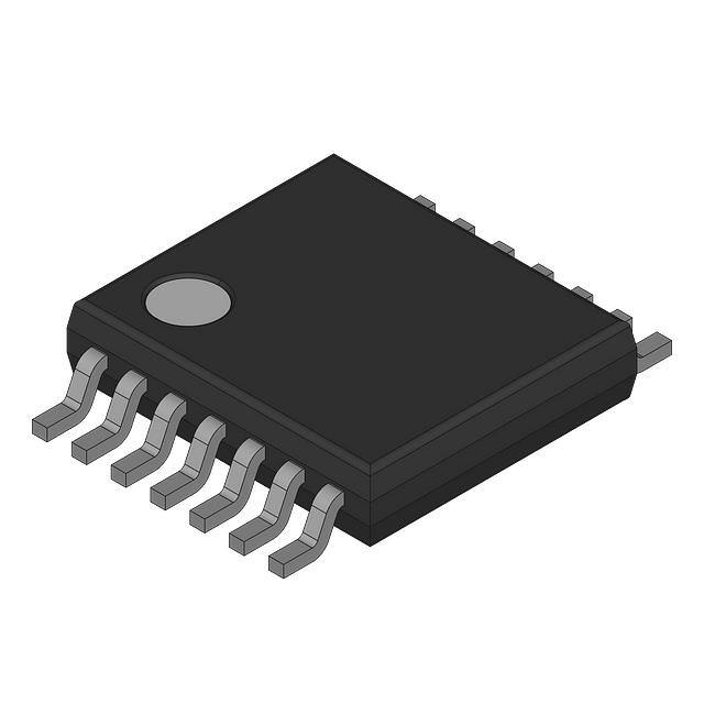
14-Lead Thin Shrink Small Outline Package (TSSOP), JEDEC MO-153,
4.4mm Wide
14-Lead Plastic Dual-In-Line Package (PDIP), JEDEC MS-001, 0.300" Wide
Device also available in Tape and Reel. Specify by appending suffix letter “X” to the ordering number.
All packages are lead free per JEDEC: J-STD-020B standard.
©1983 Fairchild Semiconductor Corporation
MM74HC74A Rev. 1.3.0
www.fairchildsemi.com
MM74HC74A — Dual D-Type Flip-Flop with Preset and Clear
February 2008
�Truth Table
Pin Assignments for DIP, SOIC, SOP and TSSOP
Inputs
Outputs
PR
CLR
CLK
D
Q
Q
L
H
X
X
H
L
H
L
X
X
L
H
H(1)
L
L
X
X
H(1)
H
H
↑
H
H
L
H
H
↑
L
L
H
H
H
L
X
Q0
Q0
Note:
Q0 = the level of Q before the indicated input conditions
were established.
1. This configuration is nonstable; that is, it will not persist
when preset and clear inputs return to their inactive
(HIGH) level.
Top View
Logic Diagram
©1983 Fairchild Semiconductor Corporation
MM74HC74A Rev. 1.3.0
www.fairchildsemi.com
2
MM74HC74A — Dual D-Type Flip-Flop with Preset and Clear
Connection Diagram
�Stresses exceeding the absolute maximum ratings may damage the device. The device may not function or be
operable above the recommended operating conditions and stressing the parts to these levels is not recommended.
In addition, extended exposure to stresses above the recommended operating conditions may affect device reliability.
The absolute maximum ratings are stress ratings only.
Symbol
Parameter
Rating
VCC
Supply Voltage
VIN
DC Input Voltage
–1.5 to VCC+1.5V
DC Output Voltage
–0.5 to VCC+0.5V
VOUT
IIK, IOK
–0.5 to +7.0V
Clamp Diode Current
±20mA
IOUT
DC Output Current, per pin
±25mA
ICC
DC VCC or GND Current, per pin
±50mA
TSTG
PD
Storage Temperature Range
–65°C to +150°C
Power Dissipation
Note 3
600mW
S.O. Package only
TL
500mW
Lead Temperature (Soldering 10 seconds)
260°C
Notes:
2. Unless otherwise specified all voltages are referenced to ground.
3. Power Dissipation temperature derating — plastic “N” package: –12mW/°C from 65°C to 85°C.
Recommended Operating Conditions
The Recommended Operating Conditions table defines the conditions for actual device operation. Recommended
operating conditions are specified to ensure optimal performance to the datasheet specifications. Fairchild does not
recommend exceeding them or designing to absolute maximum ratings.
Symbol
VCC
VIN, VOUT
TA
t r, t f
Parameter
Min.
Max.
Units
Supply Voltage
2
6
V
DC Input or Output Voltage
0
VCC
V
–40
+85
°C
Operating Temperature Range
Input Rise or Fall Times
VCC = 2.0V
1000
ns
VCC = 4.5V
500
ns
VCC = 6.0V
400
ns
©1983 Fairchild Semiconductor Corporation
MM74HC74A Rev. 1.3.0
www.fairchildsemi.com
3
MM74HC74A — Dual D-Type Flip-Flop with Preset and Clear
Absolute Maximum Ratings(2)
�TA = –40°C
to 85°C
TA = –55°C
to 125°C
Typ.
Guaranteed Limits
Symbol
Parameter
VCC (V)
VIH
Minimum HIGH
Level Input
Voltage
2.0
1.5
1.5
1.5
4.5
3.15
3.15
3.15
6.0
4.2
4.2
4.2
Maximum LOW
Level Input
Voltage
2.0
0.5
0.5
0.5
4.5
1.35
1.35
1.35
6.0
1.8
1.8
1.8
Minimum HIGH
Level Output
Voltage
2.0
2.0
1.9
1.9
1.9
4.5
4.4
4.4
4.4
6.0
5.9
5.9
5.9
VIL
VOH
VOL
Maximum LOW
Level Output
Voltage
4.5
Conditions
TA = 25°C
VIN = VIH or VIL,
|IOUT| ≤ 20µA
6.0
4.5
VIN = VIH or VIL,
|IOUT| ≤ 4.0mA
4.3
3.98
3.84
3.7
6.0
VIN = VIH or VIL,
|IOUT| ≤ 5.2mA
5.2
5.48
5.34
5.2
2.0
VIN = VIH or VIL,
|IOUT| ≤ 20µA
0
0.1
0.1
0.1
0
0.1
0.1
0.1
0
0.1
0.1
0.1
4.5
6.0
4.5
VIN = VIH or VIL,
|IOUT| ≤ 4.0mA
0.2
0.26
0.33
0.4
6.0
|VIN = VIH or VIL,
IOUT| ≤ 5.2mA
0.2
0.26
0.33
0.4
Units
V
V
V
V
IIN
Maximum Input
Current
6.0
VIN = VCC or GND
±0.1
±1.0
±1.0
µA
ICC
Maximum
Quiescent
Supply Current
6.0
VI N =VCC or GND,
IOUT = 0µA
4.0
40
80
µA
Note:
4. For a power supply of 5V ±10% the worst case output voltages (VOH, and VOL) occur for HC at 4.5V. Thus the 4.5V
values should be used when designing with this supply. Worst case VIH and VIL occur at VCC = 5.5V and 4.5V
respectively. (The VIH value at 5.5V is 3.85V.) The worst case leakage current (IIN, ICC, and IOZ) occur for CMOS at
the higher voltage and so the 6.0V values should be used.
©1983 Fairchild Semiconductor Corporation
MM74HC74A Rev. 1.3.0
www.fairchildsemi.com
4
MM74HC74A — Dual D-Type Flip-Flop with Preset and Clear
DC Electrical Characteristics(4)
�VCC = 5V, TA = 25°C, CL = 15pF, tr = tf = 6ns
Typ.
Guaranteed
Limit
Units
Maximum Operating Frequency
72
30
MHz
tPHL, tPLH
Maximum Propagation,
Delay Clock to Q or Q
10
30
ns
tPHL, tPLH
Maximum Propagation,
Delay Preset or Clear to Q or Q
17
40
ns
Minimum Removal Time,
Preset or Clear to Clock
6
5
ns
ts
Minimum Setup Time, Data to Clock
10
20
ns
tH
Minimum Hold Time, Clock to Data
0
0
ns
tW
Minimum Pulse Width Clock, Preset or Clear
8
16
ns
Symbol
fMAX
tREM
Parameter
©1983 Fairchild Semiconductor Corporation
MM74HC74A Rev. 1.3.0
Conditions
www.fairchildsemi.com
5
MM74HC74A — Dual D-Type Flip-Flop with Preset and Clear
AC Electrical Characteristics
�CL = 50 pF, tr = tf = 6ns (unless otherwise specified)
TA = 25°C
Symbol
fMAX
Parameter
Conditions
Maximum Operating
Frequency
tH
tW
Typ.
2.0
22
6
5
4
4.5
72
30
24
20
Guaranteed Limits
94
35
28
24
34
110
140
165
4.5
12
22
28
33
6.0
10
19
24
28
2.0
66
150
190
225
4.5
20
30
38
45
6.0
16
26
33
38
Minimum Removal
Time, Preset or Clear
to Clock
2.0
20
50
65
75
4.5
6
10
13
15
6.0
5
9
11
13
Minimum Setup Time
Data to Clock
2.0
35
80
100
120
4.5
10
16
20
24
6.0
8
Minimum Hold Time
Clock to Data
Minimum, Pulse Width
Clock, Preset or Clear
tTLH, tTHL Maximum Output
Rise and Fall Time
tr , tf
VCC (V)
6.0
tPHL, tPLH Maximum Propagation
Delay Preset or Clear
to Q or Q
ts
TA = –55°C
to 125°C
2.0
tPHL, tPLH Maximum Propagation
Delay Clock to Q or Q
tREM
TA = –40°C
to 85°C
Maximum Input Rise
and Fall Time
14
17
20
2.0
0
0
0
4.5
0
0
0
6.0
0
0
0
2.0
30
80
101
119
4.5
9
16
20
24
6.0
8
14
17
20
2.0
25
75
95
110
4.5V
7
15
19
22
6.0V
6
13
16
19
2.0
1000
1000
1000
4.5
500
500
500
400
400
400
6.0
CPD
Power Dissipation
Capacitance(5)
CIN
Maximum Input
Capacitance
(per flip-flop)
80
5
Units
MHz
ns
ns
ns
ns
ns
ns
ns
ns
pF
10
10
10
pF
Note:
5. CPD determines the no load dynamic power consumption, PD = CPD VCC2 f + ICC VCC, and the no load dynamic
current consumption, IS = CPD VCC f + ICC.
©1983 Fairchild Semiconductor Corporation
MM74HC74A Rev. 1.3.0
www.fairchildsemi.com
6
MM74HC74A — Dual D-Type Flip-Flop with Preset and Clear
AC Electrical Characteristics
�0.65
A
0.43TYP
14
8
B
6.4
6.10
3.2
1
PIN#1 IDENT
0.2 C B A
7
TOP VIEW
1.65
ALL LEAD TIPS
0.45
RECOMMENDED LAND PATTERN
1.2 MAX
0.30
0.19
ALL LEAD TIPS
0.1 C
0.65
SEE DETAIL A
0.90+0.15
-0.10
0.13
A B
0.20
0.09
C
C
FRONT VIEW
0.09 MIN
NOTES:
A. CONFORMS TO JEDEC REGISTRATION MO-153,
VARIATION AB, REF NOTE 6
B. DIMENSIONS ARE IN MILLIMETERS.
C. DIMENSIONS ARE EXCLUSIVE OF BURRS,
MOLD FLASH, AND TIE BAR EXTRUSIONS
D. DIMENSIONING AND TOLERANCES PER ANSI
Y14.5M, 2009.
E. LANDPATTERN STANDARD: SOP65P640X110-14M.
F. DRAWING FILE NAME: MKT-MTC14rev7.
GAGE PLANE
0.09 MIN
1.00
0.25
SEATING PLANE
DETAIL A
��8.75
8.50
A
7.62
14
8
14
B
0.65
8
4.00
3.80
6.00
1
PIN #1
IDENT.
1.27
(0.33)
TOP VIEW
5.60
7
0.51
0.35
0.25 M C B A
1.75 MAX
1.70
1
1.27
LAND PATTERN RECOMMENDATION
A
C
1.50
1.25
FRONT VIEW
0.25
0.10
0.50
0.25 x 45
R0.10
GAGE
PLANE
R0.10
0.36
8°
0°
0.90
0.50
(1.04)
0.10 C
0.25
0.19
SIDE VIEW
NOTES:
A. CONFORMS TO JEDEC MS-012,
VARIATION AB, ISSUE C
B. ALL DIMENSIONS ARE IN MILLIMETERS
C. DIMENSIONS DO NOT INCLUDE MOLD
FLASH OR BURRS
D. LAND PATTERN STANDARD:
SOIC127P600X145-14M
E. CONFORMS TO ASME Y14.5M, 2009
D. DRAWING FILENAME: MKT-M14Arev14
SEATING PLANE
DETAIL A
SCALE 16 : 1
7
�ON Semiconductor and
are trademarks of Semiconductor Components Industries, LLC dba ON Semiconductor or its subsidiaries in the United States and/or other countries.
ON Semiconductor owns the rights to a number of patents, trademarks, copyrights, trade secrets, and other intellectual property. A listing of ON Semiconductor’s product/patent
coverage may be accessed at www.onsemi.com/site/pdf/Patent−Marking.pdf. ON Semiconductor reserves the right to make changes without further notice to any products herein.
ON Semiconductor makes no warranty, representation or guarantee regarding the suitability of its products for any particular purpose, nor does ON Semiconductor assume any liability
arising out of the application or use of any product or circuit, and specifically disclaims any and all liability, including without limitation special, consequential or incidental damages.
Buyer is responsible for its products and applications using ON Semiconductor products, including compliance with all laws, regulations and safety requirements or standards,
regardless of any support or applications information provided by ON Semiconductor. “Typical” parameters which may be provided in ON Semiconductor data sheets and/or
specifications can and do vary in different applications and actual performance may vary over time. All operating parameters, including “Typicals” must be validated for each customer
application by customer’s technical experts. ON Semiconductor does not convey any license under its patent rights nor the rights of others. ON Semiconductor products are not
designed, intended, or authorized for use as a critical component in life support systems or any FDA Class 3 medical devices or medical devices with a same or similar classification
in a foreign jurisdiction or any devices intended for implantation in the human body. Should Buyer purchase or use ON Semiconductor products for any such unintended or unauthorized
application, Buyer shall indemnify and hold ON Semiconductor and its officers, employees, subsidiaries, affiliates, and distributors harmless against all claims, costs, damages, and
expenses, and reasonable attorney fees arising out of, directly or indirectly, any claim of personal injury or death associated with such unintended or unauthorized use, even if such
claim alleges that ON Semiconductor was negligent regarding the design or manufacture of the part. ON Semiconductor is an Equal Opportunity/Affirmative Action Employer. This
literature is subject to all applicable copyright laws and is not for resale in any manner.
PUBLICATION ORDERING INFORMATION
LITERATURE FULFILLMENT:
Literature Distribution Center for ON Semiconductor
19521 E. 32nd Pkwy, Aurora, Colorado 80011 USA
Phone: 303−675−2175 or 800−344−3860 Toll Free USA/Canada
Fax: 303−675−2176 or 800−344−3867 Toll Free USA/Canada
Email: orderlit@onsemi.com
© Semiconductor Components Industries, LLC
N. American Technical Support: 800−282−9855 Toll Free
USA/Canada
Europe, Middle East and Africa Technical Support:
Phone: 421 33 790 2910
Japan Customer Focus Center
Phone: 81−3−5817−1050
www.onsemi.com
1
ON Semiconductor Website: www.onsemi.com
Order Literature: http://www.onsemi.com/orderlit
For additional information, please contact your local
Sales Representative
www.onsemi.com
�


 工商网监
湘ICP备2023018690号
工商网监
湘ICP备2023018690号
