DATA SHEET
www.onsemi.com
Dual D-Type Flip-Flop with
Preset and Clear
14
1
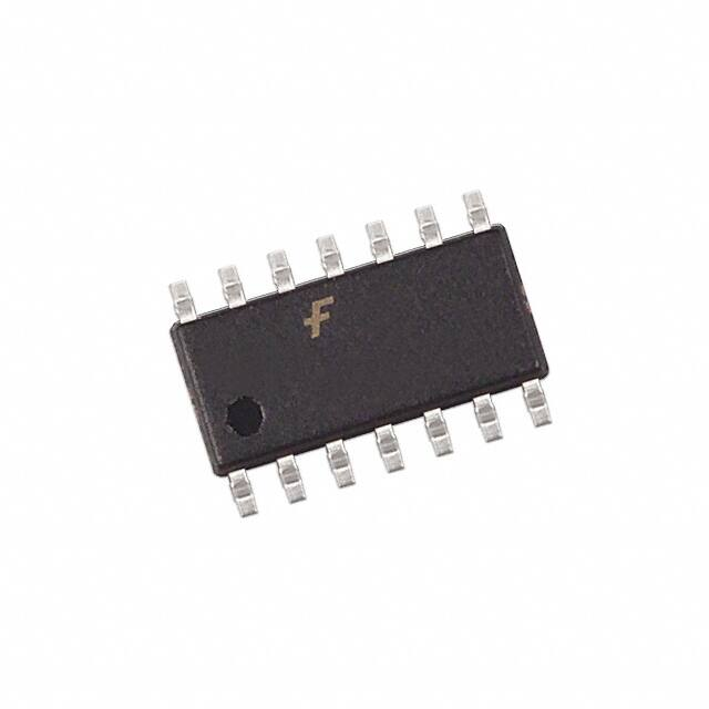
SOIC−14 NB
CASE 751A−03
MM74HCT74
14
General Description
The MM74HCT74 utilizes advanced silicon−gate CMOS
technology to achieve operation speeds similar to the equivalent
LS−TTL part. It possesses the high noise immunity and low power
consumption of standard CMOS integrated circuits, along with the
ability to drive 10 LS−TTL loads.
This flip−flop has independent data, preset, clear, and clock inputs
and Q and Q outputs. The logic level present at the data input is
transferred to the output during the positive−going transition of the
clock pulse. Preset and clear are independent of the clock and
accomplished by a low level at the appropriate input.
The 74HCT logic family is functionally and pin−out compatible
with the standard 74LS logic family. All inputs are protected from
damage due to static discharge by internal diode clamps to VCC and
ground.
MM74HCT devices are intended to interface between TTL and
NMOS components and standard CMOS devices. These parts are also
plug−in replacements for LS−TTL devices and can be used to reduce
power consumption in existing designs.
1
TSSOP−14 WB
CASE 948G
MARKING DIAGRAM
14
HCT74A
AWLYWW
1
SOIC−14 NB
14
HCT
74A
ALYW
1
TSSOP−14
Features
•
•
•
•
•
•
Typical Propagation Delay: 18 ns
Low Quiescent Current: 80 mA Maximum (74HCT Series)
Low Input Current: 1 mA Maximum
Fanout of 10 LS−TTL Loads
Meta−stable Hardened
These Devices are Pb−Free, Halide Free and are RoHS Compliant
HCT74A
A
WL, L
Y
WW, W
= Specific Device Code
= Assembly Location
= Wafer Lot
= Year
= Work Week
ORDERING INFORMATION
See detailed ordering and shipping information on page 7 of
this data sheet.
Connection Diagram
Top View
Figure 3. Pin Assignments for SOIC and TSSOP
© Semiconductor Components Industries, LLC, 1984
November, 2022 − Rev. 2
4
Publication Order Number:
MM74HCT74D
�MM74HCT74
TRUTH TABLE
Inputs
Outputs
PR
CLR
CLK
D
Q
Q
L
H
X
X
H
L
H
L
X
X
L
H
L
L
X
X
H (Note 4)
H (Note 4)
H
H
↑
H
H
L
H
H
↑
L
L
H
H
H
L
X
Q0
Q0
Q0 = the level of Q before the indicated input conditions were established.
4. This configuration is nonstable; that is, it will not persist when preset and clear inputs return to their inactive (HIGH) level.
Logic Diagram
Figure 4. Logic Diagram
ABSOLUTE MAXIMUM RATINGS (Note 5)
Symbol
Parameter
Rating
VCC
Supply Voltage
VIN
DC Input Voltage
–0.5 to VCC + 0.5 V
DC Output Voltage
–0.5 to VCC + 0.5 V
VOUT
–0.5 to +7.0 V
Clamp Diode Current
±20 mA
IOUT
DC Output Current, per Pin
±25 mA
ICC
DC VCC or GND Current, per Pin
±50 mA
IIK, IOK
TSTG
Storage Temperature Range
–65°C to +150°C
PD
Power Dissipation
TL
Lead Temperature (Soldering 10 Seconds)
S.O. Package Only
500 mW
260°C
Stresses exceeding those listed in the Maximum Ratings table may damage the device. If any of these limits are exceeded, device functionality
should not be assumed, damage may occur and reliability may be affected.
5. Unless otherwise specified all voltages are referenced to ground.
www.onsemi.com
5
�MM74HCT74
RECOMMENDED OPERATING CONDITIONS
Symbol
VCC
VIN, VOUT
Parameter
Supply Voltage
DC Input or Output Voltage
TA
Operating Temperature Range
tr, tf
Input Rise or Fall Times
Min
Max
Unit
4.5
5.5
V
0
VCC
V
–55
+125
°C
−
500
ns
Functional operation above the stresses listed in the Recommended Operating Ranges is not implied. Extended exposure to stresses beyond
the Recommended Operating Ranges limits may affect device reliability.
DC CHARACTERISTICS (VCC = 5 V ±10% (unless otherwise specified))
TA = −40°C TA = −55°C
to 85°C
to 125°C
TA = 25°C
Symbol
Parameter
Typ
Conditions
Guaranteed Limits
Unit
VIH
Minimum HIGH Level Input Voltage
2.0
2.0
2.0
V
VIL
Maximum LOW Level Input Voltage
0.8
0.8
0.8
V
VOH
Minimum HIGH Level Output Voltage
VCC
VCC – 0.1
VCC – 0.1
VCC – 0.1
V
VIN = VIH or VIL, |IOUT| = 4.0 mA,
VCC = 4.5 V
4.2
3.98
3.84
3.7
VIN = VIH or VIL, |IOUT| = 4.8 mA,
VCC = 5.5 V
5.2
4.98
4.84
4.7
0
0.1
0.1
0.1
VIN = VIH or VIL, |IOUT| = 4.0 mA,
VCC = 4.5 V
0.2
0.26
0.33
0.4
VIN = VIH or VIL, |IOUT| = 4.8 mA,
VCC = 5.5 V
0.2
0.26
0.33
0.4
VOL
Maximum LOW Level Voltage
VIN = VIH or VIL, |IOUT| = 20 mA
VIN = VIH or VIL, |IOUT| = 20 mA
V
IIN
Maximum Input Current
VIN = VCC or GND, VIH or VIL
−
±0.5
±0.5
±1.0
mA
ICC
Maximum Quiescent Supply Current
VIN = VCC or GND, IOUT = 0 mA
−
2.0
20
80
mA
VIN = 2.4 V or 0.5 V (Note 6)
−
0.3
0.4
0.5
mA
6. This is measured per input with all other inputs held at VCC or ground.
AC CHARACTERISTICS (VCC = 5.0 V, tr = tf = 6 ns, CL = 15 pF, TA = 25°C (unless otherwise noted))
Symbol
Typ
Guaranteed Limit
Unit
Maximum Operating Frequency from Clock to Q or Q
50
30
MHz
tPHL, tPLH
Maximum Propagation Delay Clock to Q or Q
18
30
ns
tPHL, tPLH
Maximum Propagation Delay from Preset or Clear to Q or Q
18
30
ns
fMAX
tREM
Parameter
Conditions
Minimum Removal Time, Preset or Clear to Clock
−
20
ns
tS
Minimum Setup Time Data to Clock
−
20
ns
tH
Minimum Hold Time Clock to Data
–3
0
ns
tW
Minimum Pulse Width Clock, Preset or Clear
8
16
ns
www.onsemi.com
6
�MM74HCT74
AC CHARACTERISTICS (VCC = 5.0 V ±10%, CL = 50 pF, tr = tf = 6 ns (unless otherwise noted))
TA = 25°C
Parameter
Symbol
fMAX
Conditions
Typ
TA = −40°C to 85°C
Guaranteed Limits
Unit
Maximum Operating Frequency
−
27
21
MHz
tPHL, tPLH
Maximum Propagation Delay from Clock to Q or Q
21
35
44
ns
tPHL, tPLH
Maximum Propagation Delay from Preset or Clear to Q or
Q
21
35
44
ns
Minimum Removal Time Preset or Clear to Clock
−
20
25
ns
tS
Minimum Setup Time Data to Clock
−
20
25
ns
tH
Minimum Hold Time Clock to Data
–3
0
0
ns
tW
Minimum Pulse Width Clock, Preset or Clear
9
16
20
ns
tr, tf
Maximum Clock Input Rise and Fall Time
−
500
500
ns
Maximum Output Rise and Fall Time
−
15
19
ns
10
−
−
pF
5
10
10
pF
tREM
tTHL, tTLH
CPD
Power Dissipation Capacitance (Note 7)
CIN
Maximum Input Capacitance
(per flip−flINop)
2
7. CPD determines the no load dynamic power consumption, PD = CPD VCC f + ICC VCC, and the no load dynamic current consumption,
IS = CPD VCC f + ICC.
ORDERING INFORMATION
Package
Shipping†
MM74HCT74M
SOIC−14, Case 751A−03
(Pb−Free, Halide−Free)
55 Units / Tube
MM74HCT74MX
SOIC−14, Case 751A−03
(Pb−Free, Halide−Free)
2500 Units / Tape & Reel
TSSOP−14, Case 948G−01
(Pb−Free, Halide Free)
2500 Units / Tape & Reel
Part Number
MM74HCT74MTCX
†For information on tape and reel specifications, including part orientation and tape sizes, please refer to our Tape and Reel Packaging
Specifications Brochure, BRD8011/D.
www.onsemi.com
7
�MECHANICAL CASE OUTLINE
PACKAGE DIMENSIONS
SOIC−14 NB
CASE 751A−03
ISSUE L
14
1
SCALE 1:1
D
DATE 03 FEB 2016
A
B
14
8
A3
E
H
L
1
0.25
B
M
DETAIL A
7
13X
M
b
0.25
M
C A
S
B
S
0.10
X 45 _
M
A1
e
DETAIL A
h
A
C
SEATING
PLANE
DIM
A
A1
A3
b
D
E
e
H
h
L
M
MILLIMETERS
MIN
MAX
1.35
1.75
0.10
0.25
0.19
0.25
0.35
0.49
8.55
8.75
3.80
4.00
1.27 BSC
5.80
6.20
0.25
0.50
0.40
1.25
0_
7_
INCHES
MIN
MAX
0.054 0.068
0.004 0.010
0.008 0.010
0.014 0.019
0.337 0.344
0.150 0.157
0.050 BSC
0.228 0.244
0.010 0.019
0.016 0.049
0_
7_
GENERIC
MARKING DIAGRAM*
SOLDERING FOOTPRINT*
6.50
NOTES:
1. DIMENSIONING AND TOLERANCING PER
ASME Y14.5M, 1994.
2. CONTROLLING DIMENSION: MILLIMETERS.
3. DIMENSION b DOES NOT INCLUDE DAMBAR
PROTRUSION. ALLOWABLE PROTRUSION
SHALL BE 0.13 TOTAL IN EXCESS OF AT
MAXIMUM MATERIAL CONDITION.
4. DIMENSIONS D AND E DO NOT INCLUDE
MOLD PROTRUSIONS.
5. MAXIMUM MOLD PROTRUSION 0.15 PER
SIDE.
14
14X
1.18
XXXXXXXXXG
AWLYWW
1
1
1.27
PITCH
XXXXX
A
WL
Y
WW
G
= Specific Device Code
= Assembly Location
= Wafer Lot
= Year
= Work Week
= Pb−Free Package
*This information is generic. Please refer to
device data sheet for actual part marking.
Pb−Free indicator, “G” or microdot “G”, may
or may not be present. Some products may
not follow the Generic Marking.
14X
0.58
DIMENSIONS: MILLIMETERS
*For additional information on our Pb−Free strategy and soldering
details, please download the ON Semiconductor Soldering and
Mounting Techniques Reference Manual, SOLDERRM/D.
STYLES ON PAGE 2
DOCUMENT NUMBER:
DESCRIPTION:
98ASB42565B
SOIC−14 NB
Electronic versions are uncontrolled except when accessed directly from the Document Repository.
Printed versions are uncontrolled except when stamped “CONTROLLED COPY” in red.
PAGE 1 OF 2
onsemi and
are trademarks of Semiconductor Components Industries, LLC dba onsemi or its subsidiaries in the United States and/or other countries. onsemi reserves
the right to make changes without further notice to any products herein. onsemi makes no warranty, representation or guarantee regarding the suitability of its products for any particular
purpose, nor does onsemi assume any liability arising out of the application or use of any product or circuit, and specifically disclaims any and all liability, including without limitation
special, consequential or incidental damages. onsemi does not convey any license under its patent rights nor the rights of others.
© Semiconductor Components Industries, LLC, 2019
www.onsemi.com
�SOIC−14
CASE 751A−03
ISSUE L
DATE 03 FEB 2016
STYLE 1:
PIN 1. COMMON CATHODE
2. ANODE/CATHODE
3. ANODE/CATHODE
4. NO CONNECTION
5. ANODE/CATHODE
6. NO CONNECTION
7. ANODE/CATHODE
8. ANODE/CATHODE
9. ANODE/CATHODE
10. NO CONNECTION
11. ANODE/CATHODE
12. ANODE/CATHODE
13. NO CONNECTION
14. COMMON ANODE
STYLE 2:
CANCELLED
STYLE 3:
PIN 1. NO CONNECTION
2. ANODE
3. ANODE
4. NO CONNECTION
5. ANODE
6. NO CONNECTION
7. ANODE
8. ANODE
9. ANODE
10. NO CONNECTION
11. ANODE
12. ANODE
13. NO CONNECTION
14. COMMON CATHODE
STYLE 4:
PIN 1. NO CONNECTION
2. CATHODE
3. CATHODE
4. NO CONNECTION
5. CATHODE
6. NO CONNECTION
7. CATHODE
8. CATHODE
9. CATHODE
10. NO CONNECTION
11. CATHODE
12. CATHODE
13. NO CONNECTION
14. COMMON ANODE
STYLE 5:
PIN 1. COMMON CATHODE
2. ANODE/CATHODE
3. ANODE/CATHODE
4. ANODE/CATHODE
5. ANODE/CATHODE
6. NO CONNECTION
7. COMMON ANODE
8. COMMON CATHODE
9. ANODE/CATHODE
10. ANODE/CATHODE
11. ANODE/CATHODE
12. ANODE/CATHODE
13. NO CONNECTION
14. COMMON ANODE
STYLE 6:
PIN 1. CATHODE
2. CATHODE
3. CATHODE
4. CATHODE
5. CATHODE
6. CATHODE
7. CATHODE
8. ANODE
9. ANODE
10. ANODE
11. ANODE
12. ANODE
13. ANODE
14. ANODE
STYLE 7:
PIN 1. ANODE/CATHODE
2. COMMON ANODE
3. COMMON CATHODE
4. ANODE/CATHODE
5. ANODE/CATHODE
6. ANODE/CATHODE
7. ANODE/CATHODE
8. ANODE/CATHODE
9. ANODE/CATHODE
10. ANODE/CATHODE
11. COMMON CATHODE
12. COMMON ANODE
13. ANODE/CATHODE
14. ANODE/CATHODE
STYLE 8:
PIN 1. COMMON CATHODE
2. ANODE/CATHODE
3. ANODE/CATHODE
4. NO CONNECTION
5. ANODE/CATHODE
6. ANODE/CATHODE
7. COMMON ANODE
8. COMMON ANODE
9. ANODE/CATHODE
10. ANODE/CATHODE
11. NO CONNECTION
12. ANODE/CATHODE
13. ANODE/CATHODE
14. COMMON CATHODE
DOCUMENT NUMBER:
DESCRIPTION:
98ASB42565B
SOIC−14 NB
Electronic versions are uncontrolled except when accessed directly from the Document Repository.
Printed versions are uncontrolled except when stamped “CONTROLLED COPY” in red.
PAGE 2 OF 2
onsemi and
are trademarks of Semiconductor Components Industries, LLC dba onsemi or its subsidiaries in the United States and/or other countries. onsemi reserves
the right to make changes without further notice to any products herein. onsemi makes no warranty, representation or guarantee regarding the suitability of its products for any particular
purpose, nor does onsemi assume any liability arising out of the application or use of any product or circuit, and specifically disclaims any and all liability, including without limitation
special, consequential or incidental damages. onsemi does not convey any license under its patent rights nor the rights of others.
© Semiconductor Components Industries, LLC, 2019
www.onsemi.com
�MECHANICAL CASE OUTLINE
PACKAGE DIMENSIONS
TSSOP−14 WB
CASE 948G
ISSUE C
14
DATE 17 FEB 2016
1
SCALE 2:1
14X K REF
0.10 (0.004)
0.15 (0.006) T U
M
T U
V
S
S
S
N
2X
14
L/2
0.25 (0.010)
8
M
B
−U−
L
PIN 1
IDENT.
N
F
7
1
0.15 (0.006) T U
NOTES:
1. DIMENSIONING AND TOLERANCING PER
ANSI Y14.5M, 1982.
2. CONTROLLING DIMENSION: MILLIMETER.
3. DIMENSION A DOES NOT INCLUDE MOLD
FLASH, PROTRUSIONS OR GATE BURRS.
MOLD FLASH OR GATE BURRS SHALL NOT
EXCEED 0.15 (0.006) PER SIDE.
4. DIMENSION B DOES NOT INCLUDE
INTERLEAD FLASH OR PROTRUSION.
INTERLEAD FLASH OR PROTRUSION SHALL
NOT EXCEED 0.25 (0.010) PER SIDE.
5. DIMENSION K DOES NOT INCLUDE DAMBAR
PROTRUSION. ALLOWABLE DAMBAR
PROTRUSION SHALL BE 0.08 (0.003) TOTAL
IN EXCESS OF THE K DIMENSION AT
MAXIMUM MATERIAL CONDITION.
6. TERMINAL NUMBERS ARE SHOWN FOR
REFERENCE ONLY.
7. DIMENSION A AND B ARE TO BE
DETERMINED AT DATUM PLANE −W−.
S
DETAIL E
K
A
−V−
K1
J J1
ÉÉÉ
ÇÇÇ
ÇÇÇ
ÉÉÉ
SECTION N−N
−W−
C
0.10 (0.004)
−T− SEATING
PLANE
H
G
D
DETAIL E
DIM
A
B
C
D
F
G
H
J
J1
K
K1
L
M
MILLIMETERS
INCHES
MIN
MAX
MIN MAX
4.90
5.10 0.193 0.200
4.30
4.50 0.169 0.177
−−−
1.20
−−− 0.047
0.05
0.15 0.002 0.006
0.50
0.75 0.020 0.030
0.65 BSC
0.026 BSC
0.50
0.60 0.020 0.024
0.09
0.20 0.004 0.008
0.09
0.16 0.004 0.006
0.19
0.30 0.007 0.012
0.19
0.25 0.007 0.010
6.40 BSC
0.252 BSC
0_
8_
0_
8_
GENERIC
MARKING DIAGRAM*
14
SOLDERING FOOTPRINT
XXXX
XXXX
ALYWG
G
7.06
1
1
0.65
PITCH
14X
0.36
14X
1.26
DIMENSIONS: MILLIMETERS
DOCUMENT NUMBER:
98ASH70246A
DESCRIPTION:
TSSOP−14 WB
A
L
Y
W
G
= Assembly Location
= Wafer Lot
= Year
= Work Week
= Pb−Free Package
(Note: Microdot may be in either location)
*This information is generic. Please refer to
device data sheet for actual part marking.
Pb−Free indicator, “G” or microdot “G”, may
or may not be present. Some products may
not follow the Generic Marking.
Electronic versions are uncontrolled except when accessed directly from the Document Repository.
Printed versions are uncontrolled except when stamped “CONTROLLED COPY” in red.
PAGE 1 OF 1
onsemi and
are trademarks of Semiconductor Components Industries, LLC dba onsemi or its subsidiaries in the United States and/or other countries. onsemi reserves
the right to make changes without further notice to any products herein. onsemi makes no warranty, representation or guarantee regarding the suitability of its products for any particular
purpose, nor does onsemi assume any liability arising out of the application or use of any product or circuit, and specifically disclaims any and all liability, including without limitation
special, consequential or incidental damages. onsemi does not convey any license under its patent rights nor the rights of others.
© Semiconductor Components Industries, LLC, 2019
www.onsemi.com
�onsemi,
, and other names, marks, and brands are registered and/or common law trademarks of Semiconductor Components Industries, LLC dba “onsemi” or its affiliates
and/or subsidiaries in the United States and/or other countries. onsemi owns the rights to a number of patents, trademarks, copyrights, trade secrets, and other intellectual property.
A listing of onsemi’s product/patent coverage may be accessed at www.onsemi.com/site/pdf/Patent−Marking.pdf. onsemi reserves the right to make changes at any time to any
products or information herein, without notice. The information herein is provided “as−is” and onsemi makes no warranty, representation or guarantee regarding the accuracy of the
information, product features, availability, functionality, or suitability of its products for any particular purpose, nor does onsemi assume any liability arising out of the application or use
of any product or circuit, and specifically disclaims any and all liability, including without limitation special, consequential or incidental damages. Buyer is responsible for its products
and applications using onsemi products, including compliance with all laws, regulations and safety requirements or standards, regardless of any support or applications information
provided by onsemi. “Typical” parameters which may be provided in onsemi data sheets and/or specifications can and do vary in different applications and actual performance may
vary over time. All operating parameters, including “Typicals” must be validated for each customer application by customer’s technical experts. onsemi does not convey any license
under any of its intellectual property rights nor the rights of others. onsemi products are not designed, intended, or authorized for use as a critical component in life support systems
or any FDA Class 3 medical devices or medical devices with a same or similar classification in a foreign jurisdiction or any devices intended for implantation in the human body. Should
Buyer purchase or use onsemi products for any such unintended or unauthorized application, Buyer shall indemnify and hold onsemi and its officers, employees, subsidiaries, affiliates,
and distributors harmless against all claims, costs, damages, and expenses, and reasonable attorney fees arising out of, directly or indirectly, any claim of personal injury or death
associated with such unintended or unauthorized use, even if such claim alleges that onsemi was negligent regarding the design or manufacture of the part. onsemi is an Equal
Opportunity/Affirmative Action Employer. This literature is subject to all applicable copyright laws and is not for resale in any manner.
PUBLICATION ORDERING INFORMATION
LITERATURE FULFILLMENT:
Email Requests to: orderlit@onsemi.com
onsemi Website: www.onsemi.com
◊
TECHNICAL SUPPORT
North American Technical Support:
Voice Mail: 1 800−282−9855 Toll Free USA/Canada
Phone: 011 421 33 790 2910
Europe, Middle East and Africa Technical Support:
Phone: 00421 33 790 2910
For additional information, please contact your local Sales Representative
�


 工商网监
湘ICP备2023018690号
工商网监
湘ICP备2023018690号
