MUR3020WTG,
MUR3040WTG,
MUR3060WTG
Switch Mode
Power Rectifiers
http://onsemi.com
These state−of−the−art devices are designed for use in switching
power supplies, inverters and as free wheeling diodes.
Features
•
•
•
•
•
•
•
•
•
•
Ultrafast 35 and 60 Nanosecond Recovery Time
175°C Operating Junction Temperature
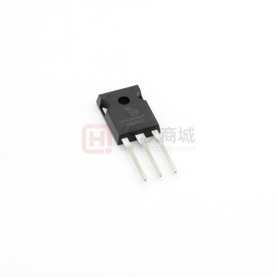
Popular TO−247 Package
High Voltage Capability to 600 V
Low Forward Drop
Low Leakage Specified @ 150°C Case Temperature
Current Derating Specified @ Both Case and Ambient Temperatures
Epoxy Meets UL 94 V−0 @ 0.125 in
High Temperature Glass Passivated Junction
These Devices are Pb−Free, Halogen Free/BFR Free and are RoHS
Compliant*
ULTRAFAST RECTIFIERS
30 AMPERES, 200−600 VOLTS
1
2, 4
3
1
2
TO−247
CASE 340AL
3
Mechanical Characteristics:
• Case: Epoxy, Molded
• Weight: 4.3 Grams (Approximately)
• Finish: All External Surfaces Corrosion Resistant and Terminal Leads
MARKING DIAGRAM
are Readily Solderable
• Lead Temperature for Soldering Purposes: 260°C Max. for 10 Seconds
• Shipped 30 Units Per Plastic Tube
MUR30x0WT
AYWWG
MUR30x0WT = Device Code
x = 2, 4 or 6
A
= Assembly Location
Y
= Year
WW
= Work Week
G
= Pb−Free Package
ORDERING INFORMATION
*For additional information on our Pb−Free strategy and soldering details, please
download the ON Semiconductor Soldering and Mounting Techniques
Reference Manual, SOLDERRM/D.
© Semiconductor Components Industries, LLC, 2014
July, 2014 − Rev. 7
1
Device
Package
Shipping
MUR3020WTG
TO−247
(Pb−Free)
30 Units/Rail
MUR3040WTG
TO−247
(Pb−Free)
30 Units/Rail
MUR3060WTG
TO−247
(Pb−Free)
30 Units/Rail
Publication Order Number:
MUR3020WT/D
�MUR3020WTG, MUR3040WTG, MUR3060WTG
MAXIMUM RATINGS (Per Leg)
Rating
Symbol
MUR3020WT
MUR3040WT
MUR3060WT
Unit
Peak Repetitive Reverse Voltage
Working Peak Reverse Voltage
DC Blocking Voltage
VRRM
VRWM
VR
200
400
600
V
Average Rectified Forward Current @ 145°C
Total Device
IF(AV)
15
30
A
Peak Repetitive Surge Current
(Rated VR, Square Wave, 20 kHz, TC = 145°C)
IFM
30
A
Nonrepetitive Peak Surge Current (Surge applied at rated load
conditions, halfwave, single phase, 60 Hz)
IFSM
Operating Junction and Storage Temperature
200
TJ, Tstg
150
150
A
°C
− 65 to +175
Stresses exceeding those listed in the Maximum Ratings table may damage the device. If any of these limits are exceeded, device functionality
should not be assumed, damage may occur and reliability may be affected.
THERMAL CHARACTERISTICS (Per Leg)
Rating
Symbol
MUR3020WT
MUR3040WT
MUR3060WT
Unit
°C/W
Maximum Thermal Resistance,
− Junction−to−Case
− Junction−to−Ambient
1.5
40
RqJC
RqJA
ELECTRICAL CHARACTERISTICS (Per Leg)
Rating
Symbol
MUR3020WT
MUR3040WT
MUR3060WT
0.85
1.05
1.12
1.25
1.4
1.7
500
10
500
10
1000
10
trr
35
60
60
IRM
0.7
Maximum Instantaneous Forward Voltage (Note 1)
(IF = 15 Amp, TC = 150°C)
(IF = 15 Amp, TC = 25°C)
VF
Maximum Instantaneous Reverse Current (Note 1)
(Rated DC Voltage, TJ = 150°C)
(Rated DC Voltage, TJ = 25°C)
iR
Maximum Reverse Recovery Time (iF = 1.0 A, di/dt = 50 Amps/ms)
Typical Peak Reverse Recovery Current
(IF = 1.0 A, di/dt = 50 A/ms)
Unit
V
mA
ns
A
Product parametric performance is indicated in the Electrical Characteristics for the listed test conditions, unless otherwise noted. Product
performance may not be indicated by the Electrical Characteristics if operated under different conditions.
1. Pulse Test: Pulse Width = 300 ms, Duty Cycle ≤ 2.0%.
http://onsemi.com
2
�MUR3020WTG, MUR3040WTG, MUR3060WTG
MUR3020WT
TJ = 150°C
100
100°C
IR , REVERSE CURRENT ( μ A)
100
25°C
50
30
10
100°C
2
1
0.5
25°C
0.2
0.1
0.05
0.02
0.01
60
80 100 120 140 160 180 200
VR, REVERSE VOLTAGE (VOLTS)
*The curves shown are typical for the highest voltage device in the voltage grouping.
Typical reverse current for lower voltage selections can be estimated from these same
curves if VR is sufficiently below rated VR.
5
3
0
1
0.5
0.3
0.2
0.1
0.2
0.4
0.6
0.8
1
1.2
vF, INSTANTANEOUS VOLTAGE (VOLTS)
1.4
1.6
14
dc
12
10
SQUARE WAVE
8
6
4
RATED VOLTAGE APPLIED
2
0
140
RqJA = 15°C/W AS OBTAINED
USING A SMALL FINNED
HEAT SINK.
10
SQUARE WAVE
dc
4
SQUARE WAVE
2 RqJA = 40°C/W
AS OBTAINED IN FREE AIR
WITH NO HEAT SINK.
0
0
20
40
60
80
100 120 140
160
TA, AMBIENT TEMPERATURE (5C)
180
200
P F(AV) , AVERAGE POWER DISSIPATION (WATTS)
I F(AV) , AVERAGE FORWARD CURRENT (AMPS)
dc
12
150
160
170
TC, CASE TEMPERATURE (5C)
180
Figure 3. Current Derating, Case (Per Leg)
14
6
40
16
Figure 1. Typical Forward Voltage (Per Leg)
8
20
Figure 2. Typical Reverse Current (Per Leg)*
2
I F(AV) , AVERAGE FORWARD CURRENT (AMPS)
i F , INSTANTANEOUS FORWARD CURRENT (AMPS)
20
TJ = 150°C
50
20
10
5
16
I
(RESISTIVE LOAD) PK = π
IAV
14
I
(CAPACITIVE LOAD) PK = 5
IAV
12
10
dc
10
8
20
6
SQUARE WAVE
4
TJ = 125°C
2
0
0
Figure 4. Current Derating, Ambient (Per Leg)
2
4
6
8
10
12
14
IF(AV), AVERAGE FORWARD CURRENT (AMPS)
Figure 5. Power Dissipation (Per Leg)
http://onsemi.com
3
16
�MUR3020WTG, MUR3040WTG, MUR3060WTG
MUR3040WTG
100
50
50
20
10
5
100°C
TJ = 150°C
30
IR , REVERSE CURRENT ( μ A)
100
25°C
10
5
100°C
25°C
2
1
0.5
0.2
0.1
0.05
0.02
0.01
0
50
100
150
200
250
300
350
400
450
5
VR, REVERSE VOLTAGE (VOLTS)
3
*The curves shown are typical for the highest voltage device in the voltage groupin
Typical reverse current for lower voltage selections can be estimated from these sam
curves if VR is sufficiently below rated VR.
2
Figure 7. Typical Reverse Current (Per Leg)*
1
0.5
0.3
0.2
0.1
0.2
0.4
0.6
0.8
1
1.2
vF, INSTANTANEOUS VOLTAGE (VOLTS)
1.4
1.6
Figure 6. Typical Forward Voltage (Per Leg)
I F(AV) , AVERAGE FORWARD CURRENT (AMPS)
i F , INSTANTANEOUS FORWARD CURRENT (AMPS)
20
TJ = 150°C
16
14
dc
12
10
SQUARE WAVE
8
6
4
RATED VOLTAGE APPLIED
2
0
140
150
160
170
TC, CASE TEMPERATURE (°C)
1
14
dc
12
10
8
6
SQUARE WAVE
RθJA = 15°C/W AS OBTAINED
USING A SMALL FINNED
HEAT SINK.
dc
4
SQUARE WAVE
2 RθJA = 40°C/W
AS OBTAINED IN FREE AIR
WITH NO HEAT SINK.
0
0
160
20
40
60
80
100 120 140
TA, AMBIENT TEMPERATURE (°C)
180
200
P F(AV) , AVERAGE POWER DISSIPATION (WATTS)
I F(AV) , AVERAGE FORWARD CURRENT (AMPS)
Figure 8. Current Derating, Case (Per Leg)
16
I
(RESISTIVE-INDUCTIVE LOAD) PK = π
IAV
I
(CAPACITIVE LOAD) PK = 5
IAV
10
14
12
dc
10
20
SQUARE WAVE
8
6
4
TJ = 125°C
2
0
0
2
4
6
8
10
12
14
IF(AV), AVERAGE FORWARD CURRENT (AMPS)
Figure 9. Current Derating, Ambient (Per Leg)
Figure 10. Power Dissipation (Per Leg)
http://onsemi.com
4
�MUR3020WTG, MUR3040WTG, MUR3060WTG
MUR3060WT
200
100
50
IR , REVERSE CURRENT ( μ A)
100
50
TJ = 150°C
30
100°C
25°C
10
100°C
2
1
0.5
25°C
0.2
0.1
0.05
0.02
150
5
3
2
0.5
0.3
0.2
0.1
0.2
0.4
0.6
0.8
1
1.2
vF, INSTANTANEOUS VOLTAGE (VOLTS)
1.4
1.6
dc
8
P F(AV) , AVERAGE POWER DISSIPATION (WATTS)
I F(AV) , AVERAGE FORWARD CURRENT (AMPS)
350
400
450
500
550
600 650
14
dc
12
SQUARE WAVE
10
8
6
4
RATED VOLTAGE APPLIED
2
0
140
RqJA = 16°C/W AS OBTAINED
FROM A SMALL TO-220
HEAT SINK.
SQUARE WAVE
6
5
dc
3
SQUARE WAVE
RqJA = 60°C/W
1 AS OBTAINED IN FREE AIR
WITH NO HEAT SINK.
0
0
20
40
60
80
100 120 140
TA, AMBIENT TEMPERATURE (5C)
2
160
180
150
160
170
TC, CASE TEMPERATURE (5C)
180
Figure 13. Current Derating, Case (Per Leg)
10
4
300
16
Figure 11. Typical Forward Voltage (Per Leg)
7
250
Figure 12. Typical Reverse Current (Per Leg)*
1
9
200
VR, REVERSE VOLTAGE (VOLTS)
*The curves shown are typical for the highest voltage device in the voltage grouping.
Typical reverse current for lower voltage selections can be estimated from these same
curves if VR is sufficiently below rated VR.
I F(AV) , AVERAGE FORWARD CURRENT (AMPS)
i F , INSTANTANEOUS FORWARD CURRENT (AMPS)
20
TJ = 150°C
20
10
5
200
16
I
(CAPACITIVE LOAD) PK = 5
IAV
14
dc
10
12
10
20
SQUARE WAVE
8
(RESISTIVE-INDUCTIVE LOAD)
IPK = π
I
AV
TJ = 125°C
6
4
2
0
0
Figure 14. Current Derating, Ambient (Per Leg)
2
4
6
8
10
12
14
IF(AV), AVERAGE FORWARD CURRENT (AMPS)
Figure 15. Power Dissipation (Per Leg)
http://onsemi.com
5
16
�1
D = 0.5
0.5
0.2
0.1
0.1
0.05
0.01
0.05
t1
t2
SINGLE PULSE
DUTY CYCLE, D = t1/t2
0.02
0.01
0.01
0.02
0.05
ZqJC(t) = r(t) RqJC
RqJC = 1.5°C/W MAX
D CURVES APPLY FOR POWER
PULSE TRAIN SHOWN
READ TIME AT T1
P(pk)
0.1
0.2
0.5
1
2
5
t, TIME (ms)
10
TJ(pk) - TC = P(pk) ZqJC(t)
20
50
Figure 16. Thermal Response
1K
500
C, CAPACITANCE (pF)
r(t), TRANSIENT THERMAL RESISTANCE (NORMALIZED)
MUR3020WTG, MUR3040WTG, MUR3060WTG
TJ = 25°C
200
100
50
20
10
1
2
5
10
20
VR, REVERSE VOLTAGE (VOLTS)
50
Figure 17. Typical Capacitance (Per Leg)
http://onsemi.com
6
100
100
200
500
1K
�MUR3020WTG, MUR3040WTG, MUR3060WTG
PACKAGE DIMENSIONS
TO−247
CASE 340AL
ISSUE A
B
A
NOTE 4
E
SEATING
PLANE
0.635
M
B A
P
A
E2/2
Q
E2
NOTE 4
D
S
NOTE 3
1
2
4
DIM
A
A1
b
b2
b4
c
D
E
E2
e
L
L1
P
Q
S
3
L1
NOTE 5
L
2X
b2
c
b4
3X
e
A1
b
0.25
NOTE 7
M
B A
M
NOTE 6
NOTES:
1. DIMENSIONING AND TOLERANCING PER ASME Y14.5M, 1994.
2. CONTROLLING DIMENSION: MILLIMETERS.
3. SLOT REQUIRED, NOTCH MAY BE ROUNDED.
4. DIMENSIONS D AND E DO NOT INCLUDE MOLD FLASH.
MOLD FLASH SHALL NOT EXCEED 0.13 PER SIDE. THESE
DIMENSIONS ARE MEASURED AT THE OUTERMOST
EXTREME OF THE PLASTIC BODY.
5. LEAD FINISH IS UNCONTROLLED IN THE REGION DEFINED BY
L1.
6. ∅P SHALL HAVE A MAXIMUM DRAFT ANGLE OF 1.5° TO THE
TOP OF THE PART WITH A MAXIMUM DIAMETER OF 3.91.
7. DIMENSION A1 TO BE MEASURED IN THE REGION DEFINED
BY L1.
M
MILLIMETERS
MIN
MAX
4.70
5.30
2.20
2.60
1.00
1.40
1.65
2.35
2.60
3.40
0.40
0.80
20.30
21.40
15.50
16.25
4.32
5.49
5.45 BSC
19.80
20.80
3.50
4.50
3.55
3.65
5.40
6.20
6.15 BSC
ON Semiconductor and the
are registered trademarks of Semiconductor Components Industries, LLC (SCILLC) or its subsidiaries in the United States and/or other countries.
SCILLC owns the rights to a number of patents, trademarks, copyrights, trade secrets, and other intellectual property. A listing of SCILLC’s product/patent coverage may be accessed
at www.onsemi.com/site/pdf/Patent−Marking.pdf. SCILLC reserves the right to make changes without further notice to any products herein. SCILLC makes no warranty, representation
or guarantee regarding the suitability of its products for any particular purpose, nor does SCILLC assume any liability arising out of the application or use of any product or circuit, and
specifically disclaims any and all liability, including without limitation special, consequential or incidental damages. “Typical” parameters which may be provided in SCILLC data sheets
and/or specifications can and do vary in different applications and actual performance may vary over time. All operating parameters, including “Typicals” must be validated for each
customer application by customer’s technical experts. SCILLC does not convey any license under its patent rights nor the rights of others. SCILLC products are not designed, intended,
or authorized for use as components in systems intended for surgical implant into the body, or other applications intended to support or sustain life, or for any other application in which
the failure of the SCILLC product could create a situation where personal injury or death may occur. Should Buyer purchase or use SCILLC products for any such unintended or
unauthorized application, Buyer shall indemnify and hold SCILLC and its officers, employees, subsidiaries, affiliates, and distributors harmless against all claims, costs, damages, and
expenses, and reasonable attorney fees arising out of, directly or indirectly, any claim of personal injury or death associated with such unintended or unauthorized use, even if such claim
alleges that SCILLC was negligent regarding the design or manufacture of the part. SCILLC is an Equal Opportunity/Affirmative Action Employer. This literature is subject to all applicable
copyright laws and is not for resale in any manner.
PUBLICATION ORDERING INFORMATION
LITERATURE FULFILLMENT:
Literature Distribution Center for ON Semiconductor
P.O. Box 5163, Denver, Colorado 80217 USA
Phone: 303−675−2175 or 800−344−3860 Toll Free USA/Canada
Fax: 303−675−2176 or 800−344−3867 Toll Free USA/Canada
Email: orderlit@onsemi.com
N. American Technical Support: 800−282−9855 Toll Free
USA/Canada
Europe, Middle East and Africa Technical Support:
Phone: 421 33 790 2910
Japan Customer Focus Center
Phone: 81−3−5817−1050
http://onsemi.com
7
ON Semiconductor Website: www.onsemi.com
Order Literature: http://www.onsemi.com/orderlit
For additional information, please contact your local
Sales Representative
MUR3020WT/D
�


 工商网监
湘ICP备2023018690号
工商网监
湘ICP备2023018690号

