NB3H5150MNGEVB
NB3H5150MNG Evaluation
Board User's Manual
Introduction
The NB3H5150MNGEVB evaluation board was developed to
provide a flexible and convenient platform to quickly evaluate and
verify the operation of the NB3H5150.
This evaluation board manual contains:
• Information on the NB3H5150 Evaluation Board
• Assembly Instructions
• Test and Measurement Setup Procedures
• Board Schematic and Bill of Materials
www.onsemi.com
EVAL BOARD USER’S MANUAL
Board Features
• Accommodates the Electrical Evaluation of the NB3H5150
• Incorporates On-Board I2C/SMBus Interface Module Powered via
a USB Connection, Minimizing Cabling
• 25 MHz Crystal is Installed (Default Input)
• Differential Inputs/Outputs Signals are Accessed via SMA
Connectors or High Impedance Probes
• LVPECL Outputs are DC Loaded and Terminated. Signals then Go
•
•
•
•
through 2:1 Baluns for Direct Connection into Phase Noise Analyzer
or High-Z Scope
LVCMOS Outputs are Series Terminated and Cap Loaded
Flexible Power Supply Combinations for Device Operation
Pin-Strap Mode Frequency Select Jumpers
Convenient and Compact Board Layout
Top View
Board must be configured before powering up.
This manual should be used in conjunction with the device data
sheet which contains full technical details on the device specifications
and operation.
Bottom View
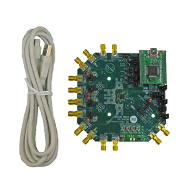
Figure 1. NB3H5150MNGEVB
Evaluation Board
© Semiconductor Components Industries, LLC, 2015
November, 2015 − Rev. 1
1
Publication Order Number:
EVBUM2300/D
�NB3H5150MNGEVB
NB3H5150MNG EVALUATION BOARD − BOARD LAYOUT MAP
Figures 2 & 3 illustrate the locations of major features and
components of the NB3H5150MNGEVB. The proceeding
information in this manual will guide the user how to
properly configure the NB3H5150 for lab testing.
LVPECL (Differential)
CLK1AB
External CLK
GND
LVPECL (Differential)
CLK2AB
LVCMOS
CLK1A
CLK1B
VDD
External CLKb
FS1
VDDO1
FS2
REFMODE
FS3
VDDO2
LVCMOS
CLK2A
CLK2B
FS4A
VDDO3
FS4B
VDDO4
LVCMOS
CLK3A
CLK3B
LVCMOS
CLK4A
CLK4B
USB/I2C
Module
LVPECL (Differential)
CLK4AB
LVPECL (Differential)
CLK3AB
Figure 2. NB3H5150MNGEVB (Top View)
Crystal
2:1 Balun × 4
3.3 V, 2.5 V, 1.8 V
Voltage Regulators
Selectable for VDDOn
Figure 3. NB3H5150MNGEVB (Bottom View)
www.onsemi.com
2
�NB3H5150MNGEVB
STEP 1: POWER SUPPLY FOR EVB
The NB3H5150MNGEVB has the flexibility to be
powered either with an external power supply or USB
module.
Table 1
describes
Jumper
Setting
J_USB_POWERS_DUT that allows
configuration.
When USB Powers DUT, VDD = 3.3 V.
for
either
Table 1. NB3H5150MNGEVB DUT POWER JUMPER SETTINGS
DUT Power
J_USB_POWERS_DUT
External Power Supply
Remove Jumper
USB/I2C
Module
Install Jumper
VDDOn
J_USB_POWERS_DUT
Figure 4. J_USB_POWERS_DUT Board Location
Power Supplies
2. VDD of the demo board using jumpers J71, J72,
J73 and J74; VDDOn = VDD.
3. Three selectable regulators: 3.3 V U401, 2.5 V
U402 and 1.8 V U403, using jumpers J71, J72, J73
and J74; VDDOn = VREGULATOR
VDD, AVDD1, AVDD2 and AVDD3 Power Pins
A single VDD test point connector is connected to the
positive power supply and powers each of the VDD and
AVDDn power supply pins.
VDDOn Power Pins
VDDOn pins can be powered individually:
1. An external power supply connected through J20,
J21, J22 and J23. Remove jumpers J71, J72, J73
and J74.
NOTE:
Figure 5 illustrates VDDOn jumper selection options.
3
Example: VDD01
Jumper to VDD
Figure 5. VDDOn Power Supply Options
www.onsemi.com
3
�NB3H5150MNGEVB
• When J58 is open, the 3.3 V, 2.5 V and 1.8 V regulators
The NB3H5150MNGEVB provides three Voltage
Regulators which can be used to power each VDDOn
separately. To power these regulators, follow Table 2 for J58
configuration.
J58 enables the optional on-board VDDOn regulators
when the device/board is powered by an external power
supply.
•
•
for VDDOn are powered by the USB.
When J58 is jumpered, the 3.3 V, 2.5 V and 1.8 V
regulators are powered by the external VDD power
supply.
When VDD = 2.5 V, VDDOn can not be 3.3 V, only
2.5 V or 1.8 V.
Table 2. VDDO VOLTAGE REGULATOR POWER
J58 − VDDO Voltage Regulator Power
VDDOn Voltage Regulator Power
USB/I2C Module
J58
VDD
Do Not Install
Use Jumper
Install
No Jumper
USB/I2C
NOTE:
Module
All four VDDOn pins must be connected to a power supply before power-up.
CAUTION:
Neglecting Table 2 configurations may cause damage to USB/I2C module.
www.onsemi.com
4
�NB3H5150MNGEVB
STEP 2: INPUT CLOCK REFERENCE FOR EVB
The NB3H5150MNGEVB has the flexibility to accept
multiple input clock references, such as: Crystal (mounted
on board), Crystal Oscillator, Signal Generator, or separate
clock integrated circuit. Table 3 describes Jumper Settings
J64 & J61 that allows for appropriate configuration.
Table 3. INPUT CLOCK REFERENCE SETTINGS
REFMODE
Input Clock
J61
J64
Crystal
Low
Position 2 & 3 Jumpered
XO
High
Position 2 & 3 Jumpered
Signal Generator
High
Position 2 & 3 Jumpered
IC
High
Position 2 & 3 Jumpered
NOTES:To use Crystal – Install R71, R72, C31 & C32 CLOAD Capacitors; Remove R69, R70, R31 & R32
To use XO – Install R69 & R70; Remove R71, R72, R31 & R32
To use Signal Generator – Install R69, R70, R31, & R32; Remove R71 & R72
J64
1
J61
2
3
Jumper Position 2 & 3
Figure 6. J61 & J64 Board Location
Crystal Input − (Default Set-Up)
External Clock Source
1. Set REFMODE = Low
2. Y1, 25 MHz crystal is installed
3. R31 & R32 are removed; R69 & R70 are not
installed.
4. R71 & R72 and C31 & C32 are installed (crystal
load capacitors).
1. Set REFMODE = High
2. Remove R71 & R72 and C31 & C32
3. R31 & R32 must be installed; and R69 & R70
must be installed.
4. R31 & R32 are 50-W to GND and are used to
terminate an external signal generator.
5. If CLK_XTAL1 and CLKb_XTAL2 pins are
driven by another IC device, remove R31 & R32.
www.onsemi.com
5
�NB3H5150MNGEVB
Figure 7. Crystal or External Clock Input Configuration Schematic
External Crystal Oscillator
i. Connect a signal generator to the J59 & J60
SMA connectors for the CLK_XTAL1 &
CLKb_XTAL2 inputs.
ii. Set appropriate input signal levels.
iii. Install 50-W termination resistors at R31 &
R32 for a signal generator termination.
iv. Remove C31 & C32. Install R69 & R70.
b. Single-Ended Input:
i. Connect a signal generator to the J59 SMA
connectors for the CLK_XTAL1 input.
ii. Ground CLKb_XTAL2.
iii. Set appropriate input signal levels.
iv. Install 50-W termination resistor at R31 for
a signal generator termination.
v. Remove C31 & C32. Install R69 & R70.
2. Set REFMODE = High
3. Connect Jumpers to J_SDA1 and J_SCL1.
a. This will connect SDA & SCL/PD to GND and
set the NB3H5150 in Pin-Strap mode.
4. Connect the CLKnA and CLKnB outputs to the
appropriate test instrument.
a. I.E. Oscilloscope, Phase Noise Analyzer,
Frequency Counter, etc.
The NB3H5150MNGEVB has features to use a 4 or 6-pin
XO, U3, in either a 5 × 7 mm or 3.2 × 5 mm package.
1. The XO can be powered separately by:
a. VDD of the demo board; connect J_OSC_VDD
HEADER 2
b. An external VDD power supply; connect
EXT_OSC_VDD at OSC_VDD.
2. Connect jumper at J75 for the XO GND pin.
3. In either option, install R73, 0-W, to power the
XO.
4. C91 & C92 are bypass capacitors for the XO VDD
power pin and are installed.
5. If using an XO, J_OSC_OE jumper header will
control the OE function of the XO,
and J_OSC_FSEL will control the frequency
select option of the XO, if needed.
Also, a crystal in a 4-pin package can be installed over the
XO footprint.
Signal Generator
1. Select Clock Input:
a. Differential Input
www.onsemi.com
6
�NB3H5150MNGEVB
REFMODE
When the REFMODE pin is Low, it selects a crystal for
the input.
When the REFMODE pin is High, it selects an external
differential or single-ended clock source for the input.
For manual control:
1. J64
a. Jumper across pins 2 & 3 to select manual
control of REFMODE and then use J61.
2. J61
a. 1 & 2 = High (VDD) – For External Clock
Source Input
b. 2 & 3 = Low (GND) – For Crystal Input
Figure 8. REFMODE Jumper Settings
www.onsemi.com
7
�NB3H5150MNGEVB
STEP 3: PIN-STRAP OR I2C MODE FOR EVB
The NB3H5150MNGEVB has the flexibility of two
methods of selecting output frequencies and level types.
Pin-Strap selections are limited to those described in data
sheet. Refer to Tables 3 & 4 of data sheet for selectable
frequencies and levels. While using I2C with provided USB
module and Software GUI, various frequency and level
types’ combinations can be generated. Table 4 describes
Jumper Settings J_SDA1, JSCL1 that allow for appropriate
configuration.
Table 4. PIN-STRAP OR I2C SETTINGS
Pin-Strap or I2C Mode
J_SDA1 & J_SCL1
Pin-Strap
Install Jumper
I2C
Remove Jumper
NOTE: For I2C Mode − Install the USB/I2C module and power-up with cable from PC, when VDD = 3.3 V.
J_SDA
J_SCL
Figure 9. J_SDA, J_SCL Board Location
Pin-Strap Operation
1. Connect a jumper across J_SDA1 and J_SCL1.
a. This will connect both SDA and SCL/PD pins
to GND.
I2C Operation
1. Remove jumpers from J_SDA1 and J_SCL1.
a. The powered I2C module will then connect
both SDA and SCL/PD pins to VDD via
pull-up resistors.
Figure 10. SDA and SCL/PD Jumper
www.onsemi.com
8
�NB3H5150MNGEVB
Control Pins
Two-Level Input Pins − REFMODE, SDA, SCL/PD and
MMC
The two-level input pins can also be controlled with H/L
jumpers.
Each control pin can be managed manually with H/L
jumper header; H = VDD, L = GND.
Tri-Level Input Pins – FSn – Frequency Select pins for CLKn
The five tri-level input pins, FS1, FS2, FS3, FS4A and
FS4B have selectable levels.
Reference Tables 3 & 4 of NB3H5150 data sheet for
pin-strap frequency settings.
The logic levels for the FSn pins can be selected manually
by using respective Jumpers.
Figure 11 is an example of control pin FS1 controlling
logic levels for CLK1.
Jumper Levels
For a HIGH Level – Put Jumper to VDD
For a LOW Level − Put Jumper to GND
For a Mid-Level – No Jumper or left open; This will enable
internal pull-up and pull-down circuits to default to
mid-level logic.
FSn pins can also be controlled through the I2C and GUI.
When controlling FSn pins via I2C, do not install jumpers on
J65, J66, J67, J68, J69, J70.
Figure 11. FS1 Jumper Setting
www.onsemi.com
9
�NB3H5150MNGEVB
STEP 4: OUTPUT LEVEL SELECTION FOR EVB
The NB3H5150MNGEVB has the flexibility of two
output types (LVPECL & LVCMOS) across four output
banks. Each output channel has the ability to drive
LVCMOS and LVPECL levels. When evaluating
LVCMOS, CLKnA & CLKnB are to be used. When
evaluating LVPECL, the NB3H5150MNGEVB has the
ability to view signal differentially and single ended.
The user must determine the output level and the respective
CLKnA, CLKnB, and CLKnAB interface in order to
configure the board correctly.
LVPECL (Differential)
CLK1AB
LVPECL (Differential)
CLK2AB
LVCMOS
CLK1A
CLK1B
LVCMOS
CLK2A
CLK2B
LVCMOS
CLK3A
CLK3B
LVCMOS
CLK4A
CLK4B
LVPECL (Differential) CLK4AB
LVPECL (Differential) CLK3AB
Figure 12. Output Selection Capabilities
CAUTION:
*CLK1, CLK2, CLK3 & CLK4 pairs are configured as both LVCMOS and LVPECL outputs.
www.onsemi.com
10
�NB3H5150MNGEVB
LVCMOS Output Configuration – Remove R1A2 and
R1B2; R1A1 and R1B1 remain installed; The LVCMOS
outputs have provisions for a series RS and a CLoad;
RS = 33-W and CLoad = 5 pF are installed.
The user must determine each output type and configure
the outputs accordingly by removing the appropriate
components to establish one signal output path.
Figure 13. LVCMOS Output Configuration
LVPECL Output Configuration – Remove R1A1 and
R1B1; R1A2 and R1B2 remain installed; R1A3 & R1A4 and
R1B3 & R1B4 are Thevenin equivalent DC load and AC
termination resistors.
Figure 14. LVPECL Output Configuration
The differential LVPECL outputs are DC loaded and AC
terminated with Thevenin resistors, capacitor-coupled into
U100, a 2:1 balun which creates a true differential signal.
This signal connects directly into a test instrument,
primarily a phase noise analyzer, an oscilloscope with
a high-Z probe, frequency counter, etc.
NOTES: In pin-strap mode, the NB3H5150 CLK1 defaults to
LVCMOS only, and CLK2 defaults to LVPECL only.
Therefore, on the EVB, remove the appropriate resistors
such that CLK1A & CLK1B defaults to LVCMOS output
configuration, and the CLK1AB SMA connector is open
(Figure 13).
Use a high-Z probe on the two single-ended outputs.
CLK2 defaults to differential LVPECL output
configuration. Remove the appropriate resistors such
that the CLK2AB SMA connector is used and
CLK2A & CLK2B SMA connectors are open (Figure 14).
www.onsemi.com
11
�NB3H5150MNGEVB
LVPECL Complementary Single Ended Output
Configuration
Option 1
1. The LVPECL outputs can be observed at the
Thevenin termination resistors, but C1A2 and
C1B2 must be removed, as the cap-coupled balun
will affect the signal at this node. Observe the two
single-ended LVPECL outputs with Hi−Z probe at
the nodes below with a high-Z probe.
The NB3H5150 EVB has the ability to observe LVPECL
waveforms single-ended using the two separate options.
Components will either need to be added or removed for
appropriate configuration. The following describes the two
options to view LVPECL as complementary single-ended
waveforms.
LVPECL Output CLKnA
Use High-Z Probe Here
LVPECL Output CLKnB
Use High-Z Probe Here
Figure 15. LVPECL Outputs − Optional Set-Up
Option 2
The LVPECL outputs can also be monitored by modifying
a few board components: remove R1A2 & R1B2, Replace
0W
R1A1 & R1B1 with 0-W resistors, remove 5-pF, install
Thevenin resistors R1A5 & R1A6 and R1B5 & R1B6.
LVPECL Output CLKnA
Use High-Z Probe Here
127 W
83 W
0W
LVPECL Output CLKnB
Use High-Z Probe Here
127 W
83 W
Figure 16. LVPECL Outputs − Optional Set-Up
www.onsemi.com
12
�NB3H5150MNGEVB
STEP 5: POWER SEQUENCE FOR EVB
USB Power Supply
The NB3H5150 EVB has the flexibility of being powered
by two different methods; external power supply or via USB
module connection.
1. Configure board according to Steps 1 through 4.
2. Connect USB cable to I2C Module
3. Monitor CLKnA & CLKnB outputs on
oscilloscope or other test instrument.
External Power Supply
1. Connect power supply cables to VCC and GND
connectors.
2. Configure board according to Steps 1 through 4.
3. Turn on VDD power supply
4. Monitor CLKnA & CLKnB outputs on
oscilloscope or other test instrument.
*When using an external clock source, board must be powered
first.
Phase Noise Analyzer
LVPECL IN
Signal Generator
GND
VDD
Oscilloscope
LVCMOS
IN
OUT
OUTb
Figure 17. Power Sequence Diagram
Graphical User Interface (GUI)
SCL/PD & SDA
The SMBus Clock (SCL/PD) and Data (SDA) pins are
exercised through the on-board I2C interface.
In order to enable the I2C control of the DUT, see Step 3.
The I2C/SMBus interface circuitry is powered separately
from the USB type-B connection and is isolated from the
device VDD and VDDOn. The SDA and SCL/PD pins can
also be externally accessed by an off-board programmer,
allowing other SMBus emulators to be used to program the
DUT. “Test-point anvils” TP5 & TP6 are available for
external control of the device with the use with mini-grabber
cables.
There is a stand-alone Graphical User Interface software
package and GUI user’s manual that will interface with the
DUT via the USB connector.
USB & I 2C/SMBus Interface
The NB3H5150 EVB has an on-board I2C/SMBus
interface module located in the lower left section of the
board.
This circuitry will interface the device with the GUI
software via the SDA and SCL/PD input pins. The GUI can
control the Frequency Select pins, output types, output
enable, and PLL ByPass Mode.
www.onsemi.com
13
�NB3H5150MNGEVB
Graphical User Interface Set-Up
All layers are constructed with FR4 dielectric material.
1. Connect the USB port on the evaluation board to
a USB port via PC cable.
2. See the stand-alone GUI instructions document.
3. Allow Windows to install the necessary drivers for
the evaluation board USB interface hardware.
4. Start the GUI program.
Layer Stack
L1 (Top) Signal
L2 Ground
L3 Power
L4 Power
L5 Ground
L6 (Bottom) Signal
•
•
•
•
•
•
Board Layout
The NB3H5150 QFN-32 Evaluation Board provides
a high bandwidth, 50-W controlled trace impedance
environment (100-W line-to-line differential) and is
implemented in six layers.
STACKUP: 6 LAYERS
Layer
Number
Layer
Name
Thickness
(Inches)
1
Top
−
Dielectric
2
IMPEDANCE
Material
W
(±5%)
Line
Width
0.0012
Copper
50, 100
0.010; 0.012
0.0080
FR−4
−
−
GND
0.0012
Copper
−
−
−
Dielectric
0.0040
FR−4
−
−
3
PWR1
0.0012
Copper
−
−
−
Dielectric
ADJUST
FR−4
−
−
4
PWR2
0.0012
Copper
−
−
−
Dielectric
0.0040
FR−4
−
−
5
GND
0.0012
Copper
−
−
−
Dielectric
0.0080
FR−4
−
−
6
Bottom
0.0012
Copper
50, 100
0.010; 0.012
Figure 18. NB3H5150MNG Evaluation Board Layer Stack-Up
www.onsemi.com
14
�A
B
C
3
2
1
GND
hdr_1x03_.100
J75
3
2
1
3
2
GND
5
1
2
3
1
2
3
.1uF
DNI
1
2
3
U4
DNI
6
5
4
6
5
4
6
OE
VDD 5
FSEL CLK/ 4
GND CLK
U3
22UF
C92
GND
J59
142−0761−861/870
3
2
1
g1
g2
g3
g4
hdr_1x03_.100
J61
GND
J60
142−0761−861/870
J_OSC_OE
J_OSC_FSEL
G4
G3
G2
G1
G5
G6
G7
G8
G4
G3
G2
G1
D
GND
g9
GND g10
GND g11
GND g12
GND
REFMODE
VDD
1
1
GND
GND
GND
GND
4
ONSEMI_NB3H5150
U1−2
GND
DNI
DNI
J64 REFMODE
R70
R69
1
1
4
2
GND
R32
49.9
GND
R31
49.9
GND
C86
.1uF
REFMODE_DUT
SDA
SCL
VDD_DUT
FS1
FS2
FS3
GND
C32
18pF
SDA
SCL
VDD_DUT
FS1
FS2
FS3
R72
0
18pF
C31
GND
Y1
25Mhz
R71
0
1
2
3
4
5
6
7
8
3
AVDD1_DUT
5
3
AVDD2_DUT
3
VDDO4_DUT
GND
C82
.1uF
CLKB_XT2
FTM
REFMODE
CLK2B
SDA
CLK2A
U1−1
SCL
VDDO2
VDD ONSEMI_NB3H5150VDDO3
FS1
CLK3A
FS2
CLK3B
FS3
MMC
GND
C85
.1uF
VDDO1_DUT
32
31
LDO1
30 AVDD1_DUT
29
LDO2
28 AVDD2_DUT
27
CLK1A
26
CLK1B
25 VDDO1_DUT
CLK_XT1
LDO1
AVDD1
LDO2
AVDD2
CLK1A
CLK1B
VDDO1
FS4A
FS4B
LDO4
AVDD3
LDO3
CLK4A
CLK4B
VDDO4
G5
G6
G7
G8
g13
GND g14
GND g15
GND g16
GND
GND
GND
GND
GND
www.onsemi.com
g5
g6
g7
g8
15
FS4A 9
FS4A
FS4B 10
FS4B
LDO4 11
LDO4
AVDD3_DUT12
AVDD3_DUT
13
14
15
VDDO4_DUT16
+
LDO3
CLK4A
CLK4B
EXT_OSC_VDD
J_OSC_VDD VDD OSC_VDD
HEADER 2
R73
DNI
1
OSC_VDD
2
C91
GND GND
C83 C84
.1uF .1uF
24
23
CLK2B
22
21 VDDO2_DUT CLK2A
20 VDDO3_DUT
19
CLK3A
18
CLK3B
17
MMC
2
R39
3.3K
GND
VDDO2_DUT
VDDO3_DUT
2
0
R40
Date:
Size
B
Title
14209
Wednesday, September 16, 2015
Document Number
1
NB3H5150 DEMO BOARD
RESERVED
1
Sheet
1
of
Rev
4
C
A
B
C
D
NB3H5150MNGEVB
SCHEMATICS
�A
B
C
5
CLK2B
CLK2A
CLK1B
CLK1A
33
R2B1
0
GND
R2B4 .1UF
83.5
C2B2
C2A2
R2B2
R2B3
127
.1UF
R2A4
83.5
R2A3
127
VDDO2_DUT
GND
R1B4 .1UF
83.5
0
R2A2
33
R2A1
33
R1B1
R1A4
83.5
C1B2
R1B2
0
.1UF
0
R1B3
127
C1A2
R1A3
127
VDDO1_DUT
R1A2
33
R1A1
4
4
U100
U200
3
2
1
5.0 pF
C2A1
5.0 pF
C2B1
GND
DNI
R2B6
VDDO2_DUT DNI R2B5
MABA−007159
GND
4
5
1
1
1
1
1
1
GND
5.0 pF
GND
DNI
R2A6
VDDO2_DUT DNI R2A5
3
2
1
C1B1
GND
DNI
R1B6
VDDO1_DUT DNI R1B5
MABA−007159
4
5
5.0 pF
C1A1
GND
DNI
R1A6
VDDO1_DUT DNI R1A5
G1
G2
G3
G4
CLK1A
GND
G8
G7
G6
G5
G1
G2
G3
G4
CLK1AB
GND
G8
G7
G6
G5
G1
G2
G3
G4
CLK1B
GND
G8
G7
G6
G5
G1
G2
G3
G4
CLK2A
GND
G8
G7
G6
G5
G1
G2
G3
G4
CLK2AB
GND
G8
G7
G6
G5
G1
G2
G3
G4
CLK2B
GND
G8
G7
G6
G5
142−0761−861/870
142−0761−861/870
142−0761−861/870
142−0761−861/870
142−0761−861/870
142−0761−861/870
3
CLK4B
CLK4A
CLK3B
CLK3A
3
33
R4B1
GND
R4B4 .1UF
83.5
C4B2
R4B2
0
.1UF
0
R4B3
127
C4A2
R4A4
83.5
R4A3
127
VDDO4_DUT
GND
R4A2
33
R4A1
33
R3B1
R3B4 .1UF
83.5
C3B2
R3B2
0
.1UF
0
R3B3
127
C3A2
R3A4
83.5
R3A3
127
VDDO3_DUT
R3A2
33
R3A1
U300
U400
Date:
Size
B
Title
1
1
1
1
CLK3A
GND
CLK3AB
GND
CLK3B
GND
CLK4A
GND
CLK4AB
GND
CLK4B
GND
1
14209
Wednesday, September 16, 2015
Document Number
1
NB3H5150 DEMO BOARD
5.0 pF
C4B1
GND
DNI
R4B6
VDDO4_DUT DNI R4B5
2
3
2
1
5.0 pF
C4A1
MABA−007159
GND
4
5
5.0 pF
GND
DNI
R4A6
VDDO4_DUT DNI R4A5
1
1
GND
C3B1
GND
DNI
R3B6
VDDO3_DUT DNI R3B5
3
2
1
5.0 pF
C3A1
GND
DNI
R3A6
DNI R3A5
MABA−007159
4
5
VDDO3_DUT
2
G1
G2
G3
G4
G8
G7
G6
G5
G1
G2
G3
G4
G8
G7
G6
G5
G1
G2
G3
G4
G8
G7
G6
G5
G1
G2
G3
G4
G8
G7
G6
G5
G1
G2
G3
G4
G8
G7
G6
G5
G1
G2
G3
G4
142−0761−861/870
142−0761−861/870
142−0761−861/870
142−0761−861/870
142−0761−861/870
16
G8
G7
G6
G5
www.onsemi.com
142−0761−861/870
D
5
Sheet2
of
4
Rev:
C
A
B
C
D
NB3H5150MNGEVB
�A
B
C
3
hdr_1x02_.100
5
1
J68
1
2
GND
3
LDO2
LDO1
FS2
VDD
FS1
VDD
J42
hdr_1x03_.100
J65
hdr_1x02_.100
2
GND
2
J40
hdr_1x03_.100
1
1
C3
.1uF
C5
.1uF
GND
1uF
C6
GND
1uF
C4
LDO4
LDO3
J50
hdr_1x03_.100
C7
.1uF
4
GND
C9
.1uF
GND
1uF
1
2
GND
J69
C10
1
2
GND
J66
1uF
C8
J44
hdr_1x03_.100
3
3
D
hdr_1x02_.100
hdr_1x02_.100
2
I/O_FS3
LDO1−4
I2C JUMPERS
MMC
VDD
FS3
VDD
J46
hdr_1x03_.100
3
J48
hdr_1x03_.100
J67
1
2
GND
3
3
J70
1
2
GND
3
4
hdr_1x02_.100
hdr_1x02_.100
2
I/O_FS4A
2
1
1
1
1
I/O_FS1
2
I/O_FS2
CLK2
FS4B
VDD
FS4A
VDD
1
2
1
2
V3V3
GND
SCL
GND
SDA
TP2
SCL
USB5V
I/O_FS4A
USB5V
USB5V
V3V3
VDD_DUT
VDD
10K
GND
3
10K
10uF
C93
R67
SCL
SDA
I/O_FS4B
RESERVED
R68
TP1
SDA
2
Date:
Size
B
Title
CN2
1
3
5
7
9
11
13
15
17
19
21
23
25
2
4
6
8
10
12
14
16
18
20
22
24
26
1
1
3
5
7
9
11
13
15
17
19
21
23
25
CN3
GND
GND
2
4
6
8
10
12
14
16
18
20
22
24
26
14209
Wednesday, September 16, 2015
Document Number
1
V3V3
of
4
Rev:
I/O_FS1
I/O_FS2
I/O_FS3
REFMODE
I/O_MMC
Sheet3
GND
10uF
NB3H5150 DEMO BOARD
2
4
6
8
10
12
14
16
18
20
22
24
26
2
C94
2
4
6
8
10
12
14
16
18
20
22
24
26
NCV1117STAT3G
1
3
5
7
9
11
13
15
17
19
21
23
25
INPUT OUTPUT
U5
V3V3 1
3
5
7
9
11
13
15
17
19
21
23
25
FT2232HQ MINI MODULE
1
2
J58
HEADER 2
1
2
J_USB_PWR_DUT
HEADER 2
HEADER 2
J_SCL1
HEADER 2
J_SDA1
2
GND
2
I/O_MMC
www.onsemi.com
I/O_FS4B
TAB
4
17
1
5
C
A
B
C
D
NB3H5150MNGEVB
�A
B
C
GND
3 REG_V1V8
4 VDD
5 REG_V3V3
3 REG_V1V8
4 VDD
5 REG_V3V3
1 VDDO2_DUT
J73
VDDO2_DUT
2 REG_V2V5
J72
5 REG_V3V3
4 VDD
3 REG_V1V8
2 REG_V2V5
J74
VDDO3_DUT
GND
C40
10uF .1uF
C74
VDDO4_DUT
5 REG_V3V3
4 VDD
3 REG_V1V8
2 REG_V2V5
1 VDDO4_DUT
AVDD3_DUT
L8
600 Ohm (100Mhz)
1 VDDO3_DUT
AVDD2_DUT
C39
10uF .1uF
C73
2 REG_V2V5
1 VDDO1_DUT
VDD_DUT
5
POWER SUPPLIES
GND
J5
DNI
C29
GND
+
VDD
4
USB5V
USB5V
HDR_5PIN_CROSS_.100 HDR_5PIN_CROSS_.100 HDR_5PIN_CROSS_.100 HDR_5PIN_CROSS_.100
J71
GND
GND
VDDO1_DUT
C38
10uF .1uF
C72
AVDD1_DUT
C12
10uF .1uF
C71
AVDD1_DUT
VDD_DUT
AVDD2_DUT
L1
L6
L7
600 Ohm (100Mhz)600 Ohm (100Mhz) 600 Ohm (100Mhz)
J4
AVDD3_DUT
D
VDD
4
C410 C411
1uF .1uF
C404 C405
1uF .1uF
VDDO1_DUT
3
2
1
GND
3
2
1
GND
GND
4
5
4
5
3
NCP4586DSN18T1G
CE/CE NC
GND
VIN VOUT
U403
NCP4586DSN33T1G
CE/CE NC
GND
VIN VOUT
U401
C69
10uF .1uF
C70
VDDO1_DUT
J76
1uF
C409
J77
1uF
C403
REG_V1V8
REG_V3V3 USB5V
GND
C67
10uF .1uF
VDDO2_DUT
C68
C407 C408
1uF .1uF
VDDO2_DUT
L3
600 Ohm (100Mhz)
GND
3
2
1
4
5
2
NCP4688DSN25T1G
CE/CE NC
GND
VIN VOUT
U402
GND
C65
10uF .1uF
VDDO3_DUT
C66
Date:
Size
B
Title
1uF
C406
J78
VDDO3_DUT
L4
600 Ohm (100Mhz)
VDDO4_DUT
14209
Wednesday, September 16, 2015
Document Number
1
NB3H5150 DEMO BOARD
REG_V2V5
GND
C63
10uF .1uF
VDDO4_DUT
C64
1
L5
600 Ohm (100Mhz)
J23
J22
J21
L2
600 Ohm (100Mhz)
VDDO4
VDDO3
VDDO2
J20
2
VDDO1
3
1
18
1
www.onsemi.com
1
5
Sheet4
of
4
Rev:
C
A
B
C
D
NB3H5150MNGEVB
�NB3H5150MNGEVB
BILL OF MATERIALS
Table 5. NB3H5150MNGEVB BILL OF MATERIALS
MM_ICN#
COMP_DEVICE_TYPE
COMP_VALUE
SOURCE
SOURCE_PN#
QTY
REFDES
80−111−00666
CAP, CER, 0.1 mF, 50 V,
10%, X5R, 0402
0.1 mF
Digi-Key
445−5942−1−ND
8
C1A2, C1B2, C2A2,
C2B2, C3A2, C3B2,
C4A2, C4B2
80−111−00219
Cap, Chip, 18 pF, 0402,
10 V, ±2%
18 pF
Digi-Key
478−4435−1−ND
2
C31, C32
80−111−00031
Cap, Chip, 1 mF, 0603,
10V, 10%, X7R
1 mF
SMEC
MCCB105K1NRT
10
C4, C6, C8, C10, C403,
C404, C406, C407, C409,
C410
80−111−00147
CAP, CER, 0.1 mF, 50 V,
10%, X7R, 0603
0.1 mF
Digi-Key
490−1519−1−ND
17
C12, C38, C39, C40, C63,
C65, C67, C69, C82, C83,
C84, C85, C86, C92,
C405, C408, C411
80−111−00536
Cap, Chip, 5.0 pF, 0603,
50 V
5.0 pF
Digi-Key
GRM1885C1H5R0CZ01D
8
C1A1, C1B1, C2A1,
C2B1, C3A1, C3B1,
C4A1, C4B1
80−111−00255
Cap, Chip, 0.1 mF, 0805,
50 V, 5% X7R
0.1 mF
Digi-Key
MOUSER 581−05055C104J
1
C3
80−111−00796
Cap, Cer, 1206, 50 V,
0.1 mF, X7R, 10%
0.1 mF
Digi-Key
478−1556−1−ND
3
C5, C7, C9
80−111−00074
Cap, Chip, 10 mF, 1210,
10 V, 10%, X5R
10 mF
Digi-Key
587−1370−1−ND
8
C64, C66, C68, C70, C71,
C72, C73, C74
DNI
CAP_DNI_TANTB
DNI
DNI
DNI
1
C29
80−111−00197
Cap, Chip, 22 mF,
Tant “D”, 25 V 10%
22 mF
Digi-Key
478−1729−1−ND
1
C91
0805N
RES_DNI_0805
DNI
DNI
DNI
1
R73
DNI
Res, Chip, 49.9 W, 0402,
1/16 W, 1%
49.9 W
Digi-Key
P49.9LCT−ND
80−114−00163
2
R31, R32
80−114−01607
Res SMD 3.3 kW 1%
1/16 W 0402
3.3 kW
Digi-Key
RHM3.3KCDTR−ND
1
R39
80−114−00052
Res, Chip, 0 W, 0402,
1/16 W, 5%
0W
Digi-Key
311−0.0JRTR−ND
9
R40, R71, R72, R2A2,
R2B2, R3A2, R3B2,
R4A2, R4B2
DNI
Res, Chip, 0 W, 0402,
1/16 W, 5%
0W
Digi-Key
311−0.0JRTR−ND
2
R1A2, R1B2
0402N
RES_0_1/16W_5%_
0402
DNI
DNI
DNI
2
R69, R70
80−114−00473
Res, Chip, 33 W, 0402,
1/16 W, 5%
33 W
SMEC
RC73L2Z330JT
2
R1A1, R1B1
DNI
Res, Chip, 33 W, 0402,
1/16 W, 5%
33 W
SMEC
RC73L2Z330JT
6
R2A1, R2B1, R3A1,
R3B1, R4A1, R4B1
80−114−01612
Res SMD 127 W 1%
1/16 W 0402
127 W
Digi-Key
541−127LDKR−ND
8
R1A3, R1B3, R2A3,
R2B3, R3A3, R3B3,
R4A3, R4B3
0402S1
RES_DNI_0402
DNI
DNI
DNI
16
R1A5, R1A6, R1B5,
R1B6, R2A5, R2A6,
R2B5, R2B6, R3A5,
R3A6, R3B5, R3B6,
R4A5, R4A6, R4B5, R4B6
80−114−01460
Res 10 kW 1/10 W 1%
0603 SMD
10 kW
Digi-Key
P10.0KHCT−ND
2
R67, R68
80−114−01628
Res SMD 82 W 0.1%
0.15 W 0805
82.5 W, 0603
Digi-Key
ERA−6AEB820V;
P82DACT−ND
8
R1A4, R1B4, R2A4,
R2B4, R3A4, R3B4,
R4A4, R4B4
80−118−00259
IND_FERRITE−BEAD_60
0OHM_100MHZ*
600 W (100 MHz)
Digi-Key
587−1846−1−ND
8
L1, L2, L3, L4, L5, L6, L7,
L8
80−118−00260
TRANSFORMER
MABA−007159
Digi-Key
1465−1302−1−ND
4
U100, U200, U300, U400
80−080−00330
CONN SMA JACK 50 W
EDGE MNT
SMA 142−0761−861
Digi-Key
J805−ND
14
CLK1A, CLK1AB, CLK1B,
CLK2A, CLK2AB, CLK2B,
CLK3A, CLK3AB, CLK3B,
CLK4A, CLK4AB, CLK4B,
J59, J60
80−112−00108
Connector, Header,
50 Pos, 0.100″
HDR_1x01
Samtec
TSW−150−14−G−S
3
J76, J77, J78
DNI
Connector, Header,
50 Pos, 0.100″
hdr_1x02_.100
Samtec
TSW−150−14−G−S
6
J65, J66, J67, J68, J69,
J70
80−112−00108
Connector, Header,
50 Pos, 0.100″
hdr_1x03_.100
Samtec
TSW−150−14−G−S
13
J40, J42, J44, J46, J48,
J50, J61, J62, J63, J64,
J75, J_OSC_FSEL,
J_OSC_OE
www.onsemi.com
19
�NB3H5150MNGEVB
Table 5. NB3H5150MNGEVB BILL OF MATERIALS (continued)
MM_ICN#
COMP_DEVICE_TYPE
COMP_VALUE
SOURCE
SOURCE_PN#
QTY
REFDES
80−112−00249
CONN HEADER FMAL
26PS.1″ DL GOLD
26 pis conn
Digi-Key
S7116−ND
2
CN2, CN3
80−112−00108
HDR_5PIN_CROSS_.100
_HEADER, MAL
HDR_1x01(5 pin)
Samtec
TSW−150−14−G−S
4
J71, J72, J73, J74
80−112−00108
Connector, Header,
50 Pos, 0.100″
hdr_1x02_.100
Samtec
TSW−150−14−G−S
5
J58, J_OSC_VDD,
J_SCL1, J_SDA1,
J_USB_PWR_DUT
DNI
OSC_ON_NBXDBA014_
CLCC_7X5_254_D
DNI
DNI
DNI
1
U3
DNI
OSC_ECS_SUBMINIATU
RE_OSC_MINI_6
DNI
DNI
DNI
1
U4
80−112−00199
TEST POINT, PC, MULTI
PURPOSE, RED
TP RED
Digi-Key
5010K−ND
6
J4, J5, J20, J21, J22, J23
80−112−00148
TEST POINT, PC, MULTI
PURPOSE, BLK
TP BLK
Digi-Key
5011K−ND
1
EXT_OSC_VDD
80−112−00148
TEST POINT, PC, MULTI
PURPOSE, BLK
TP BLK
Digi-Key
5011K−ND
1
TP1
80−112−00148
TEST POINT, PC, MULTI
PURPOSE, BLK
TP BLK
Digi-Key
5011K−ND
1
TP2
80−113−00905
Crystal, CTS, 25 MHz, TH
25 MHz
Digi-Key
ABL−25.000MHZ−B2F
1
Y1
80−116−00527
IC REG LDO 3.3 V 0.15 A
SOT23−5
3.3 V
Digi-Key
NCP4586DSN33T1G−ND
1
U401
80−116−00526
IC REG LDO 2.5 V 0.15 A
SOT23−5
2.5 V
Digi-Key
NCP4688DSN25T1GOSCT−N
D
1
U402
80−116−00528
IC REG LDO 1.8 V 0.15 A
SOT23−5
1.8 V
Digi-Key
MIC5247−1.8YM5TR
1
U403
80−116−00549
IC REG LDO ADJ 1 A
SOT223
Digi-Key
NCV1117STAT3G
1
U5
CSP
ONSEMI_NB3H5150_SK
T_MM_50−000−0
QFM
ON Semiconductor
NB3H5150
1
U1
80−080−00327
Conn Jumper
Jumper
Digi-Key
S9341−ND
28
80−080−00337
USB Cable − USB A
Mini-B 1.8M Frost White
DNI
88732−8800
1
80−113−00906
USB Hi-Speed FT2232H
Evaluation Module
DNI
FT2232H Mini Module
1
www.onsemi.com
20
�onsemi,
, and other names, marks, and brands are registered and/or common law trademarks of Semiconductor Components Industries, LLC dba “onsemi” or its affiliates
and/or subsidiaries in the United States and/or other countries. onsemi owns the rights to a number of patents, trademarks, copyrights, trade secrets, and other intellectual property. A
listing of onsemi’s product/patent coverage may be accessed at www.onsemi.com/site/pdf/Patent−Marking.pdf. onsemi is an Equal Opportunity/Affirmative Action Employer. This
literature is subject to all applicable copyright laws and is not for resale in any manner.
The evaluation board/kit (research and development board/kit) (hereinafter the “board”) is not a finished product and is not available for sale to consumers. The board is only intended
for research, development, demonstration and evaluation purposes and will only be used in laboratory/development areas by persons with an engineering/technical training and familiar
with the risks associated with handling electrical/mechanical components, systems and subsystems. This person assumes full responsibility/liability for proper and safe handling. Any
other use, resale or redistribution for any other purpose is strictly prohibited.
THE BOARD IS PROVIDED BY ONSEMI TO YOU “AS IS” AND WITHOUT ANY REPRESENTATIONS OR WARRANTIES WHATSOEVER. WITHOUT LIMITING THE FOREGOING,
ONSEMI (AND ITS LICENSORS/SUPPLIERS) HEREBY DISCLAIMS ANY AND ALL REPRESENTATIONS AND WARRANTIES IN RELATION TO THE BOARD, ANY
MODIFICATIONS, OR THIS AGREEMENT, WHETHER EXPRESS, IMPLIED, STATUTORY OR OTHERWISE, INCLUDING WITHOUT LIMITATION ANY AND ALL
REPRESENTATIONS AND WARRANTIES OF MERCHANTABILITY, FITNESS FOR A PARTICULAR PURPOSE, TITLE, NON−INFRINGEMENT, AND THOSE ARISING FROM A
COURSE OF DEALING, TRADE USAGE, TRADE CUSTOM OR TRADE PRACTICE.
onsemi reserves the right to make changes without further notice to any board.
You are responsible for determining whether the board will be suitable for your intended use or application or will achieve your intended results. Prior to using or distributing any systems
that have been evaluated, designed or tested using the board, you agree to test and validate your design to confirm the functionality for your application. Any technical, applications or
design information or advice, quality characterization, reliability data or other services provided by onsemi shall not constitute any representation or warranty by onsemi, and no additional
obligations or liabilities shall arise from onsemi having provided such information or services.
onsemi products including the boards are not designed, intended, or authorized for use in life support systems, or any FDA Class 3 medical devices or medical devices with a similar
or equivalent classification in a foreign jurisdiction, or any devices intended for implantation in the human body. You agree to indemnify, defend and hold harmless onsemi, its directors,
officers, employees, representatives, agents, subsidiaries, affiliates, distributors, and assigns, against any and all liabilities, losses, costs, damages, judgments, and expenses, arising
out of any claim, demand, investigation, lawsuit, regulatory action or cause of action arising out of or associated with any unauthorized use, even if such claim alleges that onsemi was
negligent regarding the design or manufacture of any products and/or the board.
This evaluation board/kit does not fall within the scope of the European Union directives regarding electromagnetic compatibility, restricted substances (RoHS), recycling (WEEE), FCC,
CE or UL, and may not meet the technical requirements of these or other related directives.
FCC WARNING – This evaluation board/kit is intended for use for engineering development, demonstration, or evaluation purposes only and is not considered by onsemi to be a finished
end product fit for general consumer use. It may generate, use, or radiate radio frequency energy and has not been tested for compliance with the limits of computing devices pursuant
to part 15 of FCC rules, which are designed to provide reasonable protection against radio frequency interference. Operation of this equipment may cause interference with radio
communications, in which case the user shall be responsible, at its expense, to take whatever measures may be required to correct this interference.
onsemi does not convey any license under its patent rights nor the rights of others.
LIMITATIONS OF LIABILITY: onsemi shall not be liable for any special, consequential, incidental, indirect or punitive damages, including, but not limited to the costs of requalification,
delay, loss of profits or goodwill, arising out of or in connection with the board, even if onsemi is advised of the possibility of such damages. In no event shall onsemi’s aggregate liability
from any obligation arising out of or in connection with the board, under any theory of liability, exceed the purchase price paid for the board, if any.
The board is provided to you subject to the license and other terms per onsemi’s standard terms and conditions of sale. For more information and documentation, please visit
www.onsemi.com.
PUBLICATION ORDERING INFORMATION
LITERATURE FULFILLMENT:
Email Requests to: orderlit@onsemi.com
onsemi Website: www.onsemi.com
◊
TECHNICAL SUPPORT
North American Technical Support:
Voice Mail: 1 800−282−9855 Toll Free USA/Canada
Phone: 011 421 33 790 2910
www.onsemi.com
1
Europe, Middle East and Africa Technical Support:
Phone: 00421 33 790 2910
For additional information, please contact your local Sales Representative
�


 工商网监
湘ICP备2023018690号
工商网监
湘ICP备2023018690号
