NB3L208KMNGEVB
NB3L208K
Evaluation Board
User's Manual
www.onsemi.com
Introduction
The NB3L208K is a differential 1:8 Clock fanout buffer
with High-speed Current Steering Logic (HCSL) outputs.
Inputs can directly accept differential LVPECL, LVDS and
HCSL signals. Single-ended LVPECL, HCSL, LVCMOS,
or LVTTL levels are accepted with a proper external VTH
reference supply. These signals will be translated to HCSL
and eight identical copies of Clock will be distributed,
operating up to 350 MHz.
This manual should be used in conjunction with the device
datasheet, which contains full technical details on the device
specifications and operation.
EVAL BOARD USER’S MANUAL
•
•
•
•
•
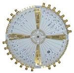
Top View
This evaluation board manual contains:
Information on the NB3L208K Evaluation Board
Block Diagram and Board Schematic
Assembly Instructions
Test and Measurement Setup Procedures
Bill of Materials
Bottom View
Figure 1. NB3L208KMNGEVB Top and Bottom View
© Semiconductor Components Industries, LLC, 2016
April, 2016 − Rev. 1
1
Publication Order Number:
EVBUM2295/D
�NB3L208KMNGEVB
QUICK START LAB SET-UP USER’S GUIDE
Equipment Required
1. DC Power Supply
2. Oscilloscope
3. Phase Noise Analyzer
4. Connectors for DC Power Supply
5. 50-W SMA Connectors for I/Os
Block Diagram
Power Supply
VDD
GND
Generator
Agilent E5052B
SSA Signal
Source Analyzer
Tek DPO70404
CH1 CH2 CH3 CH4
Balun
VDD
GND
CLK_IN
CLK_IN
DIF_0−7
DIF_0−7#
NB3L208K
DIF_0−7
DIF_0−7#
Note: Balun Connected to Outputs Only during Phase Noise Testing.
Figure 2. Time and Frequency Domain Block Diagram
Power Supplies
HCSL Outputs
Each VDD, VDD_0 (VX on board), GND_0 (DUTGND
on board) and SMAGND power supply has a separate
side-launch banana jack located on bottom side of the test
board (as shown in Figure 1).
HCSL outputs are typically loaded and terminated with
a series resistor (RSERIES) = 33-W and 50-W to ground. This
can be easily accomplished by connecting the HCSL outputs
to the 50-W internal impedance in the oscilloscope. There
are on-board RSERIES = 33-W termination resistors installed
for each HCSL output.
50 W to Ground via
SMA Connector to
Oscilloscope
RSERIES = 33 W
Figure 3. Set-Up for HCSL Output
www.onsemi.com
2
�3
24
33 W
OE#_[5:4]
OE#_[3:2]
OE#_[1:0]
VDD
IREF
GND_0
GND_0
VDD_0
VDD_0
Figure 4. NB3L208KEVB Schematic
www.onsemi.com
29
28
27
R3 475 W
26
25
C4 0.1 mF
SMAGND
GND_0
SMAGND
OE#_[7:6]
32
31
30
SMAGND
DIF_0
DIF_0#
DIF_1
DIF_1#
DIF_2
DIF_2#
DIF_3
DIF_3#
C5 0.1 mF
SMAGND
EP TIED TO
DUT GND
DIF_4
VDD_0
SMAGND
23
33 W
DIF_4#
DIF_5
DIF_5#
VDD_0
SMAGND
22
33 W
33 W
CLK_IN
SMAGND
SMAGND
C6
10 mF
20
21
16
33 W
15
DIF_6
14
GND
DIF_6#
C3 0.1 mF
13
19
C2 0.1 mF
CLK_IN#
33 W
12
18
11
33 W
9
DIF_7
DIF_7#
C1 0.1 mF
17
SMAGND
33 W
33 W
33 W
33 W
33 W
6
5
4
3
2
33 W
33 W
7
1
33 W
8
SMAGND
33 W
SMAGND
10
SMAGND
SMAGND
SMAGND
SMAGND
SMAGND
SMAGND
R2 50 W
R1 50 W
SMAGND
SMAGND
SMAGND
SMAGND
SMAGND
SMAGND
SMAGND
SMAGND
SMAGND
NB3L208KMNGEVB
�NB3L208KMNGEVB
Test and Measurement Setup Procedures
Power-Up Sequence
1. Connect VDD and VDD_0 (VX on board) of
the NB3L208K to DC source with power supply
cables (do not turn power on, yet).
2. Connect SMAGND and DUTGND to
the appropriate DC source. For differential HCSL
inputs, both SMAGND and DUTGND are
connected together.
3. Connect the outputs of the generator to
the CLK_IN & CLK_IN# inputs with 50-W
connectors. For phase noise test, low noise
generator is required to ensure the best additive
RMS Phase jitter of the DUT.
4. Connect the DIF_n/DIF_n# outputs to the
appropriate oscilloscope channel. The board does
not have 50-W output termination, thus use of the
probes with 50-W termination is required.
1. Turn on DUT power supply.
2. Setup the generator VIH, VIL levels to set up
the inputs to desired inputs levels, i.e differential
LVPECL, LVDS, and HCSL signals or
Single-ended LVPECL, HCSL, LVCMOS,
or LVTTL. For differential HCSL inputs,
VIL = 0 V and VIH = 700 mV.
3. Monitor DIF_n/DIF_n# outputs on oscilloscope.
www.onsemi.com
4
�NB3L208KMNGEVB
BILL OF MATERIALS
Table 1. NB3L208KMNGEVB BILL OF MATERIALS
Component
Qty.
Description
Manufacturer
Part Number
SMA Connector
22
Edge Mount
Johnson
142−0711−821
Banana Jack Connector
2
Red − Side Launch
Deltron
571−0500
Mouser #164−6219
Banana Jack Connector
1
Black − Side Launch
Deltron
571−0100
Mouser #164−6218
Banana Jack Connector
1
Green − Side Launch
Deltron
Chip Resistor
9
0-Q 0603
Vishay
CRCW06030000Z0EA
Digi-Key
541−0.0GTR−ND
Chip Resistor
16
33-Q 0402
Panasonic
ERJ−2RKF33R0X
Digi-Key
ERJ−2RKF33R0X
Chip Resistor
4
50-Q, 0603
Vishay
FC0603E50R0BTBST1
Digi-Key
FC0603−50BFTR−ND
Chip Resistor
1
475-Q 0603
Vishay
TNPW0603475RBEEA
Digi-Key
541−2027−2−ND
Capacitor
2
10 mF ±10%, Case “C” 25 V or 16 V
KEMET
T491C106K025AT
T491C106K016AS
Chip Capacitor
5
0.1 mF ±10%, 0603
AVX
0603C104KAT2A
www.avx.com
Digi-Key
478−1129−1−ND
Stand-Off
4
Standoff, 4−40 1/4 × 5/8
Keystone
1808
Digi-Key
1808K−ND
Screw
4
Screw, 4−40 × 0.25, PHP
Building Fasteners
PMS 440 0025 PH
Digi-Key
H342−ND
Evaluation Board
1
NB3L208KEVB
QFN−32 Evaluation Board
ON Semiconductor
NB3L208KEVB
Device Under Test
1
DUT
ON Semiconductor
NB3L208K
Mouser
NOTE: Components are available through most distributors, i.e. www.newark.com, www.Digikey.com.
www.onsemi.com
5
Web Site
www.onsemi.com
�onsemi,
, and other names, marks, and brands are registered and/or common law trademarks of Semiconductor Components Industries, LLC dba “onsemi” or its affiliates
and/or subsidiaries in the United States and/or other countries. onsemi owns the rights to a number of patents, trademarks, copyrights, trade secrets, and other intellectual property. A
listing of onsemi’s product/patent coverage may be accessed at www.onsemi.com/site/pdf/Patent−Marking.pdf. onsemi is an Equal Opportunity/Affirmative Action Employer. This
literature is subject to all applicable copyright laws and is not for resale in any manner.
The evaluation board/kit (research and development board/kit) (hereinafter the “board”) is not a finished product and is not available for sale to consumers. The board is only intended
for research, development, demonstration and evaluation purposes and will only be used in laboratory/development areas by persons with an engineering/technical training and familiar
with the risks associated with handling electrical/mechanical components, systems and subsystems. This person assumes full responsibility/liability for proper and safe handling. Any
other use, resale or redistribution for any other purpose is strictly prohibited.
THE BOARD IS PROVIDED BY ONSEMI TO YOU “AS IS” AND WITHOUT ANY REPRESENTATIONS OR WARRANTIES WHATSOEVER. WITHOUT LIMITING THE FOREGOING,
ONSEMI (AND ITS LICENSORS/SUPPLIERS) HEREBY DISCLAIMS ANY AND ALL REPRESENTATIONS AND WARRANTIES IN RELATION TO THE BOARD, ANY
MODIFICATIONS, OR THIS AGREEMENT, WHETHER EXPRESS, IMPLIED, STATUTORY OR OTHERWISE, INCLUDING WITHOUT LIMITATION ANY AND ALL
REPRESENTATIONS AND WARRANTIES OF MERCHANTABILITY, FITNESS FOR A PARTICULAR PURPOSE, TITLE, NON−INFRINGEMENT, AND THOSE ARISING FROM A
COURSE OF DEALING, TRADE USAGE, TRADE CUSTOM OR TRADE PRACTICE.
onsemi reserves the right to make changes without further notice to any board.
You are responsible for determining whether the board will be suitable for your intended use or application or will achieve your intended results. Prior to using or distributing any systems
that have been evaluated, designed or tested using the board, you agree to test and validate your design to confirm the functionality for your application. Any technical, applications or
design information or advice, quality characterization, reliability data or other services provided by onsemi shall not constitute any representation or warranty by onsemi, and no additional
obligations or liabilities shall arise from onsemi having provided such information or services.
onsemi products including the boards are not designed, intended, or authorized for use in life support systems, or any FDA Class 3 medical devices or medical devices with a similar
or equivalent classification in a foreign jurisdiction, or any devices intended for implantation in the human body. You agree to indemnify, defend and hold harmless onsemi, its directors,
officers, employees, representatives, agents, subsidiaries, affiliates, distributors, and assigns, against any and all liabilities, losses, costs, damages, judgments, and expenses, arising
out of any claim, demand, investigation, lawsuit, regulatory action or cause of action arising out of or associated with any unauthorized use, even if such claim alleges that onsemi was
negligent regarding the design or manufacture of any products and/or the board.
This evaluation board/kit does not fall within the scope of the European Union directives regarding electromagnetic compatibility, restricted substances (RoHS), recycling (WEEE), FCC,
CE or UL, and may not meet the technical requirements of these or other related directives.
FCC WARNING – This evaluation board/kit is intended for use for engineering development, demonstration, or evaluation purposes only and is not considered by onsemi to be a finished
end product fit for general consumer use. It may generate, use, or radiate radio frequency energy and has not been tested for compliance with the limits of computing devices pursuant
to part 15 of FCC rules, which are designed to provide reasonable protection against radio frequency interference. Operation of this equipment may cause interference with radio
communications, in which case the user shall be responsible, at its expense, to take whatever measures may be required to correct this interference.
onsemi does not convey any license under its patent rights nor the rights of others.
LIMITATIONS OF LIABILITY: onsemi shall not be liable for any special, consequential, incidental, indirect or punitive damages, including, but not limited to the costs of requalification,
delay, loss of profits or goodwill, arising out of or in connection with the board, even if onsemi is advised of the possibility of such damages. In no event shall onsemi’s aggregate liability
from any obligation arising out of or in connection with the board, under any theory of liability, exceed the purchase price paid for the board, if any.
The board is provided to you subject to the license and other terms per onsemi’s standard terms and conditions of sale. For more information and documentation, please visit
www.onsemi.com.
PUBLICATION ORDERING INFORMATION
LITERATURE FULFILLMENT:
Email Requests to: orderlit@onsemi.com
onsemi Website: www.onsemi.com
◊
TECHNICAL SUPPORT
North American Technical Support:
Voice Mail: 1 800−282−9855 Toll Free USA/Canada
Phone: 011 421 33 790 2910
www.onsemi.com
1
Europe, Middle East and Africa Technical Support:
Phone: 00421 33 790 2910
For additional information, please contact your local Sales Representative
�


 工商网监
湘ICP备2023018690号
工商网监
湘ICP备2023018690号
