NBA3N206SDGEVB
NBA3N206SDGEVB
Evaluation Board
User's�Manual
www.onsemi.com
Introduction
The NBA3N206S is a 3.3 V differential Multipoint
(M−LVDS) line Driver and Receiver. NBA3N206S
supports Simplex or Half Duplex bus configurations.
The NBA3N206S has Type−2 receivers that detect the
bus state with as little as 50 mV of differential input voltage
over a common−mode voltage range of −1 V to 3.4 V.
Type−2 receivers include an offset threshold of 0.1 V to
provide a detectable voltage under open−circuit, idle−bus,
and other fault conditions.
The NBA3N206SDGEVB evaluation board was
developed to accommodate the NBA3N206S device. This
evaluation board was designed to provide a flexible and
convenient platform to quickly evaluate, characterize and
verify the operation of the NBA3N206S.
EVAL BOARD USER’S MANUAL
This manual should be used in conjunction with the device
datasheet which contains full technical details on the device
specifications and operation.
Evaluation Board User’s Manual Contents:
•
•
•
•
•
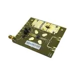
Top View
NBA3N206S Evaluation Board Information
Board Features
Board Layout Map
Test and Measurement Setup Procedures
Board Schematic and Bill of Materials
Bottom View
Figure 1. NBA3N206SDGEVB Evaluation Board
© Semiconductor Components Industries, LLC, 2015
April, 2015 − Rev. 0
1
Publication Order Number:
EVBUM2298/D
�NBA3N206SDGEVB
Section 1: Board Features
• Board supplied includes an 8−Pin SOIC.
• Board is configured to operate from a single VCC
Layer Stack
The NBA3N206SDGEVB SOIC−8 Evaluation Board
provides a high bandwidth, 50 W controlled trace impedance
environment (100 W line−to−line differential) and is
implemented in four layers.
• L1 (Top) Signal
• L2 SMA Ground
• L3 VCC and DUT Ground
• L4 (Bottom) Power Supply Bypass Capacitors, Control
Pin Traces and Banana Jacks
supply and a single GND supply.
• Single−ended and differential inputs/outputs are
•
•
•
•
•
•
accessed via SMA connectors or high impedance
probes.
Board may be configured for bus operation as:
1. Point−to−Point with Simplex Single Termination
2. Point−to−Point with Simplex Parallel Termination
3. Multipoint Two−Node with Single Termination
4. Multipoint Two−Node with Parallel Termination
Two 100 W Parallel Termination resistors are mounted
on each bus (Driver/Receiver) transceiver I/O pin pair.
Resistors may be removed for added configuration
flexibility.
All layers are constructed with FR4 dielectric material.
The first layer is the primary signal layer, including all
of the differential inputs and outputs.
The second layer is a ground plane. It is dedicated for
the SMA ground plane.
The third layer is a dedicated power plane. A portion of
the 3rd layer is designated for the device VCC and
DUTGND power planes.
Figure 2. Four Layer Stack−up
Section 2: Board Layout Map
Top View
Bottom View
Figure 3. NBA3N206SDGEVB Evaluation Board
www.onsemi.com
2
�NBA3N206SDGEVB
Table 1. LOAD BOARD CONNECTIONS AND COMPONENTS
Transceiver
Device Pin
VCC2
Board
U1 (8 Pin)
U1 Pin 8
VCC2 Power Supply connection point to U1
Function
VCC2 Anvil
U1 (8 Pin)
U1 Pin 8
Alternative connection point for VCC2
SMAGND2
U1 (8 Pin)
−
U1 SMA (J7/8/9/10/21/22) ground shields connection point
SMAGND2 Anvil
U1 (8 Pin)
−
Alternative connection point for U1 SMA shields
DUTGND2
U1 (8 Pin)
U1 Pin 5
U1 DUT ground pin
DUTGND2 Anvil
U1 (8 Pin)
U1 Pin 5
Alternative connection point for U1 DUT ground pin
J7 R
U1 (8 Pin)
U1 Pin 1
U1 R input (Note 1)
J8 D
U1 (8 Pin)
U1 Pin 4
U1 D input
J9 B
U1 (8 Pin)
U1 Pin 7
U1 B input/output (Note 1)
J10 A
U1 (8 Pin)
U1 Pin 6
U1 B input/output (Note 1)
J21 DE
U1 (8 Pin)
U1 Pin 3
U1 DE input (Note 1)
J22 REb
U1 (8 Pin)
U1 Pin 2
U1 REb input (Note 1)
P3 Header
U1 (8 Pin)
U1 Pins 6, 7
TP3
U1 (8 Pin)
U1 Pin 1
Test Point for U1 R input
TP4
U1 (8 Pin)
U1 Pin 4
Test Point for U1 D input
W3 Pad
U1 (8 Pin)
U1 Pin 2
Program point for U1 Reb
W4 Pad
U1 (8 Pin)
U1 Pin 3
Program point for U1 DE
*R12
U1 (8 Pin)
U1 Pin 1
U1 15pF R pin
R13
U1 (8 Pin)
U1 Pin 1
U1 0 W R pin
R14
U1 (8 Pin)
U1 Pin 4
U1 D input optional termination location
R15
U1 (8 Pin)
U1 Pins 6, 7
U1 100 W termination location
R16
U1 (8 Pin)
U1 Pins 6, 7
U1 100 W termination location
R17
U1 (8 Pin)
U1 Pins 7
U1 0 W A pin
R18
U1 (8 Pin)
U1 Pins 6
U1 0 W B pin
U2 Connection Header for A & B
*Replaced with CL=15pF capacitor
1. Not populated on board
www.onsemi.com
3
�NBA3N206SDGEVB
Section 3: Test and Management Setup Procedures
4. Apply LVCMOS Input Signal to D. (See datasheet
for appropriate levels)
5. Monitor Differential Bus Voltage VAB with a
Differential Probe
6. Monitor Receiver Output VR with a Hi−Z Probe
Basic Operation Setup
1. Set VCC to 3.3V
2. Set DE, Move Jumper to Logic High
3. Set REb, Move Jumper to Logic Low
Hi-Z Probe
Differential Probe
Figure 4. NBA3N206S Evaluation Board Test Block Diagram
Equipment Used (or equivalent)
1. Generator (HP 8133A or similar)
2. Oscilloscope (Tektronix TDS8000 or similar)
3. Power Supply (Agilent #6624A DC or similar)
4. Digital Voltmeter
5. Differential Probe
6. Hi−Z Probe
www.onsemi.com
4
�NBA3N206SDGEVB
Test Configurations
Simplex Theory Configurations: Data flow is
unidirectional and Point−to−Point from one Driver to one
Receiver. NBA3N206SDG devices provide a high signal
current allowing long drive runs and high noise immunity.
Single terminated interconnects yield high amplitude levels.
Parallel terminated interconnects yield typical MLVDS
amplitude levels and minimize reflections. See Figures 5
and 6. NBA3N206SDG can be used as a driver or as a
receiver.
Figure 5. Point−to−Point Simplex Single Termination
Figure 6. Parallel−Terminated Simplex
Simplex Multidrop Theory Configurations: Data flow
is unidirectional from one Driver with one or more
Receivers (Multiple boards required). Single terminated
interconnects yield high amplitude levels. Parallel
terminated interconnects yield typical MLVDS amplitude
levels and minimize reflections. Header P3 may be used as
needed to interconnect transceivers to each other or to a bus.
See Figures 1, 7, and 8. A NBA3N206SDG can be used as
the driver or as a receiver.
Figure 7. Multidrop or Distributed Simplex with Single Termination
Figure 8. Multidrop or Distributed Simplex with Double Termination
Half Duplex Multinode Multipoint Theory
Configurations: Data flow is unidirectional and selected
from one of multiple possible Drivers to multiple Receives.
One “Two Node” multipoint connection can be
accomplished with a single board. Multipoint connection
with more than two nodes require multiple boards. Parallel
terminated interconnects yield typical MLVDS amplitude
levels and minimize reflections. Header P3 may be used as
needed to interconnect transceivers to each other or to a bus.
See Figure 9. NBA3N206SDG can be used as a driver or as
a receiver.
www.onsemi.com
5
�NBA3N206SDGEVB
Figure 9. Multinode Multipoint Half Duplex (requires Double Termination)
Output Waveforms
Driver
Input
Receiver
Output
Differential
Bus
Voltage
Figure 10. High Impedance Output Termination
Figure 10 shows typical NBA3N206S waveforms. The
Driver Input is supplied by a 100 Mbps data signal via an
HP8133A generator. The Receiver Output (VR) can be
monitored using a Hi−Z probe; the Differential Bus Voltage
(VAB) can be monitored using a Differential probe.
www.onsemi.com
6
�NBA3N206SDGEVB
Section 4: Board Schematic and Bill of Materials
Board Schematic
Figure 11. Board Schematic
Table 2. BILL OF MATERIALS AND LAMINATION STACKUP
Component
Designation
Case
Value
Manufacturer
Part Number
U1
ON Semiconductor
NBA3N206S
J18
Deltron
571−0100
Banana Jacks − Black
1
J17
Deltron
571−0500
Banana Jacks − Red
1
J8
Johnson
#142−0711−821
SMA Connector Side
Launch Narrow
1
P3
AMP
4−103239−0x2
Header (make from
4−103239−0)
1
Keystone
5015
Anvil Clips
6
W3, W4
FCI
68000−103HLF
3 Pin Header
2
TP3, TP4
3M
961102−6404−AR
2 Pin Header
2
VCC2, SMAGND2,
DUTGND2
Description
Qty
1
R14
O603
50 W
Panasonic
Precision Thick Film
Chip Resistor
1
R15, R16
O603
100 W
Panasonic
Precision Thick Film
Chip Resistor
2
R13, R17, R18
O603
0W
Panasonic
Precision Thick Film
Chip Resistor
1
10 mF
KEMET
C1210X106K3RACTU
Chip Capacitor
1
15 pF
Murata
GRM1555C1E150JA01D
Chip Capacitor
1
C4
C11
0603
www.onsemi.com
7
�onsemi,
, and other names, marks, and brands are registered and/or common law trademarks of Semiconductor Components Industries, LLC dba “onsemi” or its affiliates
and/or subsidiaries in the United States and/or other countries. onsemi owns the rights to a number of patents, trademarks, copyrights, trade secrets, and other intellectual property. A
listing of onsemi’s product/patent coverage may be accessed at www.onsemi.com/site/pdf/Patent−Marking.pdf. onsemi is an Equal Opportunity/Affirmative Action Employer. This
literature is subject to all applicable copyright laws and is not for resale in any manner.
The evaluation board/kit (research and development board/kit) (hereinafter the “board”) is not a finished product and is not available for sale to consumers. The board is only intended
for research, development, demonstration and evaluation purposes and will only be used in laboratory/development areas by persons with an engineering/technical training and familiar
with the risks associated with handling electrical/mechanical components, systems and subsystems. This person assumes full responsibility/liability for proper and safe handling. Any
other use, resale or redistribution for any other purpose is strictly prohibited.
THE BOARD IS PROVIDED BY ONSEMI TO YOU “AS IS” AND WITHOUT ANY REPRESENTATIONS OR WARRANTIES WHATSOEVER. WITHOUT LIMITING THE FOREGOING,
ONSEMI (AND ITS LICENSORS/SUPPLIERS) HEREBY DISCLAIMS ANY AND ALL REPRESENTATIONS AND WARRANTIES IN RELATION TO THE BOARD, ANY
MODIFICATIONS, OR THIS AGREEMENT, WHETHER EXPRESS, IMPLIED, STATUTORY OR OTHERWISE, INCLUDING WITHOUT LIMITATION ANY AND ALL
REPRESENTATIONS AND WARRANTIES OF MERCHANTABILITY, FITNESS FOR A PARTICULAR PURPOSE, TITLE, NON−INFRINGEMENT, AND THOSE ARISING FROM A
COURSE OF DEALING, TRADE USAGE, TRADE CUSTOM OR TRADE PRACTICE.
onsemi reserves the right to make changes without further notice to any board.
You are responsible for determining whether the board will be suitable for your intended use or application or will achieve your intended results. Prior to using or distributing any systems
that have been evaluated, designed or tested using the board, you agree to test and validate your design to confirm the functionality for your application. Any technical, applications or
design information or advice, quality characterization, reliability data or other services provided by onsemi shall not constitute any representation or warranty by onsemi, and no additional
obligations or liabilities shall arise from onsemi having provided such information or services.
onsemi products including the boards are not designed, intended, or authorized for use in life support systems, or any FDA Class 3 medical devices or medical devices with a similar
or equivalent classification in a foreign jurisdiction, or any devices intended for implantation in the human body. You agree to indemnify, defend and hold harmless onsemi, its directors,
officers, employees, representatives, agents, subsidiaries, affiliates, distributors, and assigns, against any and all liabilities, losses, costs, damages, judgments, and expenses, arising
out of any claim, demand, investigation, lawsuit, regulatory action or cause of action arising out of or associated with any unauthorized use, even if such claim alleges that onsemi was
negligent regarding the design or manufacture of any products and/or the board.
This evaluation board/kit does not fall within the scope of the European Union directives regarding electromagnetic compatibility, restricted substances (RoHS), recycling (WEEE), FCC,
CE or UL, and may not meet the technical requirements of these or other related directives.
FCC WARNING – This evaluation board/kit is intended for use for engineering development, demonstration, or evaluation purposes only and is not considered by onsemi to be a finished
end product fit for general consumer use. It may generate, use, or radiate radio frequency energy and has not been tested for compliance with the limits of computing devices pursuant
to part 15 of FCC rules, which are designed to provide reasonable protection against radio frequency interference. Operation of this equipment may cause interference with radio
communications, in which case the user shall be responsible, at its expense, to take whatever measures may be required to correct this interference.
onsemi does not convey any license under its patent rights nor the rights of others.
LIMITATIONS OF LIABILITY: onsemi shall not be liable for any special, consequential, incidental, indirect or punitive damages, including, but not limited to the costs of requalification,
delay, loss of profits or goodwill, arising out of or in connection with the board, even if onsemi is advised of the possibility of such damages. In no event shall onsemi’s aggregate liability
from any obligation arising out of or in connection with the board, under any theory of liability, exceed the purchase price paid for the board, if any.
The board is provided to you subject to the license and other terms per onsemi’s standard terms and conditions of sale. For more information and documentation, please visit
www.onsemi.com.
PUBLICATION ORDERING INFORMATION
LITERATURE FULFILLMENT:
Email Requests to: orderlit@onsemi.com
onsemi Website: www.onsemi.com
◊
TECHNICAL SUPPORT
North American Technical Support:
Voice Mail: 1 800−282−9855 Toll Free USA/Canada
Phone: 011 421 33 790 2910
www.onsemi.com
1
Europe, Middle East and Africa Technical Support:
Phone: 00421 33 790 2910
For additional information, please contact your local Sales Representative
�


 工商网监
湘ICP备2023018690号
工商网监
湘ICP备2023018690号
