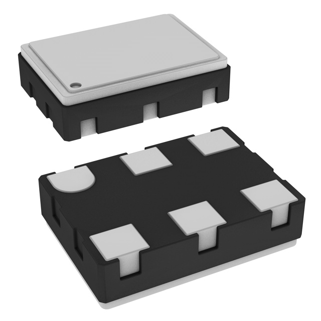
NBVSPA015 Series 3.3 V, LVDS Voltage-Controlled Clock Oscillator (VCXO) PureEdget Product Series
The NBVSPXXXX voltage−controlled crystal oscillator (VCXO) devices are designed to meet today’s requirements for 3.3 V LVDS clock generation applications. These devices use a high Q fundamental mode crystal and Phase Locked Loop (PLL) multiplier to provide a wide range of frequencies from 60 MHz to 700 MHz (factory configurable per user specifications) with a pullable range of ±100 ppm and a frequency stability of ±50 ppm. The silicon−based PureEdge t products design provides users with exceptional frequency stability and reliability. They produce an ultra low jitter and phase noise LVDS differential output. The NBVSPXXXX series devices are a member of ON Semiconductor’s PureEdget clock family that provides accurate and precision clock generation solutions. Available in the industry standard 5.0 x 7.0 x 1.8 mm and in a new smaller 3.2 x 5.0 x 1.2 mm SMD (CLCC) package on 16 mm tape and reel in quantities of 1,000.
Features
http://onsemi.com MARKING DIAGRAMS
6 PIN CLCC LN SUFFIX CASE 848AB
NBVSPXXXX XXX.XXXX AWLYYWWG
6 PIN CLCC LU SUFFIX CASE 848AC NBVSPXXXX XXX.XXXX A WL YY WW G
NBVSPXXXX XXX.XXXX AWLYYWWG
• • • • • • • • • • • • • • • •
LVDS Differential Output Uses High Q Fundamental Mode Crystal Ultra Low Jitter and Phase Noise − 0.5 ps (12 kHz − 20 MHz) Factory Configurable Frequencies from 60 MHz to 700 MHz (see Standard Frequencies in the Ordering Information Table on page 6) Pullable Range Minimum of ±100 ppm Frequency Stability of ±50 ppm Control Voltage with Positive Slope Voltage Control Linearity of ±10% Hermetically Sealed Ceramic SMD Packages of size 5.0 x 7.0 x 1.8 mm and 3.2 x 5.0 x 1.2 mm Operating Range: 3.3 V ±10% These Devices are Pb−Free and are RoHS Compliant Networking SONET 10 Gigabit Ethernet Networking Base Stations Broadcasting
= NBVSPXXXX (±50 ppm) = Output Frequency (MHz) = Assembly Location = Wafer Lot = Year = Work Week = Pb−Free Package
ORDERING INFORMATION
See detailed ordering and shipping information in the package dimensions section on page 6 of this data sheet.
Applications
© Semiconductor Components Industries, LLC, 2010
December, 2010 − Rev. 1
1
Publication Order Number: NBVSPA015/D
�NBVSPA015 Series
VDD 6 CLK CLK 54
Crystal 20−30 MHz 1 VC
PLL Clock Multiplier LVDS 2 OE 3 GND
Figure 1. Simplified Logic Diagram
VC OE GND 1 2 3 6 5 4 VDD CLK CLK
Figure 2. Pin Connections (Top View) Table 1. PIN DESCRIPTION
Pin No. 1 2 3 4 5 6 Symbol VC (Note 1) OE GND CLK CLK VDD I/O Analog Input LVTTL/LVCMOS Control Input Power Supply LVDS Output LVDS Output Power Supply Description Analog control voltage input pin that adjusts output oscillation frequency. f0 =VC = 1.65 V Output Enable Pin. When left floating pin defaults to logic HIGH and output is active. See OE pin description Table 2. Ground at 0 V. Electrical and Case Ground. Non−Inverted Clock Output. Typically loaded with 100 W receiver termination resistor across differential pair. Inverted Clock Output. Typically loaded with 100 W receiver termination resistor across differential pair. Positive Power Supply Voltage. Voltage should not exceed 3.3 V ±10%.
1. Control voltage has a positive slope with a typical linearity of ±10%; VC = 1.65 V ± 1 V.
Table 2. OUTPUT ENABLE TRI−STATE FUNCTION
OE Pin Open HIGH Level LOW Level Output Pins Active Active High Z
Table 3. ATTRIBUTES
Characteristic Input Default State Resistor ESD Protection Human Body Model Machine Model Value 170 kW 2 kV 200 V
Meets or Exceeds JEDEC Standard EIA/JESD78 IC Latchup Test 2. For additional Moisture Sensitivity information, refer to Application Note AND8003/D.
http://onsemi.com
2
�NBVSPA015 Series
Table 4. MAXIMUM RATINGS
Symbol VDD VIN IOSC TA Tstg Tsol Parameter Positive Power Supply Control Input (VC and OE) Output Short Circuit Current CLK to CLK CLK or CLK to GND Operating Temperature Range Storage Temperature Range Wave Solder See Figure 4 Continuous Continuous Condition 1 GND = 0 V VIN ≤ VDD + 200 mV VIN ≥ GND − 200 mV 12 24 −40 to +85 −55 to +120 260 Condition 2 Rating 4.6 Units V V mA °C °C °C
Stresses exceeding Maximum Ratings may damage the device. Maximum Ratings are stress ratings only. Functional operation above the Recommended Operating Conditions is not implied. Extended exposure to stresses above the Recommended Operating Conditions may affect device reliability.
Table 5. DC CHARACTERISTICS (VDD = 3.3 V ±10%, GND = 0 V, TA = −40°C to +85°C) (Note 3)
Symbol IDD VIH VIL IIH IIL DVOD VOS DVOS VOH VOL VOD Characteristic Power Supply Current OE and FSEL Input HIGH Voltage OE and FSEL Input LOW Voltage Input HIGH Current Input LOW Current Change in Magnitude of VOD for Complementary Output States Offset Voltage Change in Magnitude of VOS for Complementary Output States Output HIGH Voltage Output LOW Voltage Differential Output Voltage 900 250 (Note 4) OE OE (Note 4) 2000 GND − 300 −100 −100 0 1125 0 1 1425 1075 450 1 Conditions Min. Typ. 75 Max. 100 VDD 800 +100 +100 25 1375 25 1600 Units mA mV mV mA mA mV mV mV mV mV mV
NOTE: Device will meet the specifications after thermal equilibrium has been established when mounted in a test socket or printed circuit board with maintained transverse airflow greater than 500 Ifpm. Electrical parameters are guaranteed only over the declared operating temperature range. Functional operation of the device exceeding these conditions is not implied. Device specification limit values are applied individually under normal operating conditions and not valid simultaneously. 3. Measurement taken with outputs terminated with 100 ohm across differential pair. See Figure 3. 4. Parameter guaranteed by design verification not tested in production.
http://onsemi.com
3
�NBVSPA015 Series
Table 6. AC CHARACTERISTICS (VDD = 3.3 ±10%, GND = 0 V, TA = −40°C to +85°C) (Note 5)
Symbol fCLKOUT Characteristic Output Clock Frequency Conditions NBVSPA019 NBVSPA027 NBVSPA018 NBVSPA017 NBVSPA024 NBVSPA015 NBVSPA042 Df tjit(f) tjitter Frequency Stability – NBVSPAXXX RMS Phase Jitter Cycle to Cycle, RMS Cycle to Cycle, Peak−to−Peak Period, RMS Period, Peak−to−Peak tOE/OD FP VC(bw) tDUTY_CYCLE tR tF tstart Output Enable/Disable Time Crystal Pullability (Note 7) Control Voltage Bandwidth Output Clock Duty Cycle (Measured at Cross Point) Output Rise Time (20% and 80%) Output Fall Time (80% and 20%) Start−up Time Aging 1st Year 0 V ≤ VC ≤ 3.3 V −3 dB ±100 20 45 50 245 245 1 55 400 400 5 3 1 (Note 6) 12 kHz to 20 MHz 1000 Cycles 1000 Cycles 10,000 Cycles 10,000 Cycles 0.4 3 15 2 10 Min. Typ. 125.00 148.50 155.52 156.25 160.00 200.00 74.25 ±50 0.9 8 30 4 20 200 ppm ps ps ps ps ps ns ppm KHz % ps ps ms ppm Max. Units MHz
Every Year After 1st
NOTE: Device will meet the specifications after thermal equilibrium has been established when mounted in a test socket or printed circuit board with maintained transverse airflow greater than 500 Ifpm. Electrical parameters are guaranteed only over the declared operating temperature range. Functional operation of the device exceeding these conditions is not implied. Device specification limit values are applied individually under normal operating conditions and not valid simultaneously. 5. Measurement taken with outputs terminated with 100 ohm across differential pair. See Figure 3. 6. Parameter guarantees 10 years of aging. Includes initial stability at 25°C, shock, vibration and first year aging. 7. Gain transfer is positive with a rate of 130 ppm/V.
Table 7. PHASE NOISE PERFORMANCE FOR NBVSPXXXX
Parameter fNOISE Characteristic Output Phase−N oise Performa nce Condition 100 Hz of Carrier 1 kHz of Carrier 10 kHz of Carrier 100 kHz of Carrier 1 MHz of Carrier 10 MHz of Carrier 74.25 MHZ −94 −122 −132 −132 −142 −160 125.00 MHZ −90 −117 −128 −128 −136 −159 148.50 MHz −90 −116 −126 −126 −136 −159 155.52 MHz −90 −116 −126 −126 −134 −159 156.25 MHZ −90 −116 −126 −126 −134 −159 160.00 MHz −90 −116 −126 −126 −135 −159 200.00 MHZ −91 −117 −127 −127 −135 −159 Units dBc/Hz dBc/Hz dBc/Hz dBc/Hz dBc/Hz dBc/Hz
http://onsemi.com
4
�NBVSPA015 Series
Table 8. RELIABILITY COMPLIANCE
Parameter Shock Mechanical Mechanical Mechanical Mechanical Solderability Vibration Standard Method MIL−STD−833, Method 2002, Condition B MIL−STD−833, Method 2003 MIL−STD−202, Method 215 MIL−STD−833, Method 2007, Condition A MIL−STD−833, Method 1011, Condition A
ÁÁÁÁÁÁÁÁÁÁÁÁÁÁÁÁÁÁÁÁÁÁÁÁÁÁÁÁÁÁÁÁÁ Á Á ÁÁÁÁÁÁÁÁÁÁÁÁÁÁ Á Á ÁÁÁÁÁÁÁÁÁÁÁÁÁÁÁÁÁÁÁÁÁÁÁÁÁÁÁÁÁÁÁÁÁ Á Á ÁÁÁÁÁÁÁÁÁÁÁÁÁÁÁÁÁÁÁÁÁÁÁÁÁÁÁÁÁÁÁÁÁ Á Á ÁÁÁÁÁÁÁÁÁÁÁÁÁÁÁÁÁÁÁÁÁÁÁÁÁÁÁÁÁÁÁÁÁ Á Á ÁÁÁÁÁÁÁÁÁÁÁÁÁÁÁÁÁÁÁÁÁÁÁÁÁÁÁÁÁÁÁÁÁ Á Á ÁÁÁÁÁÁÁÁÁÁÁÁÁÁÁÁÁÁÁÁÁÁÁÁÁÁÁÁÁÁÁÁÁ Á Á ÁÁÁÁÁÁÁÁÁÁÁÁÁÁÁÁÁÁÁÁÁÁÁÁÁÁÁÁÁÁÁÁÁ Á Á ÁÁÁÁÁÁÁÁÁÁÁÁÁÁÁÁÁÁÁÁÁÁÁÁÁÁÁÁÁÁÁÁÁ Á Á ÁÁÁÁÁÁÁÁÁÁÁÁÁÁÁÁÁÁÁÁÁÁÁÁÁÁÁÁÁÁÁÁÁ ÁÁÁÁÁÁÁÁÁÁÁÁÁÁÁÁÁÁÁÁ Á ÁÁÁÁÁÁÁÁÁÁÁÁÁÁÁÁÁÁÁÁÁÁÁÁÁÁÁÁÁÁÁÁÁ Á Á ÁÁÁÁÁÁÁÁÁÁÁÁÁÁÁÁÁÁÁÁÁÁÁÁÁÁÁÁÁÁÁÁÁ Á Á
Solvent Resistance Thermal Shock Environment Environment Moisture Level Sensitivity MSL1 260°C per IPC/JEDEC J−STD−020D NBVSPAXXX CLK Driver Device CLK Zo = 50 W Zo = 50 W 100 W D D Receiver Device
Figure 3. Typical Termination for Output Driver and Device Evaluation
Temperature (°C) 260 217
temp. 260°C 20 − 40 sec. max. peak 3°C/sec. max. ramp−up
6°C/sec. max.
cooling
175 150
pre−heat reflow 60�180 sec. 60�150 sec. Time
Figure 4. Recommended Reflow Soldering Profile
http://onsemi.com
5
�NBVSPA015 Series
Table 9. ORDERING INFORMATION
Device Output Frequency (MHz) 5.0 x 7.0 x 1.8 mm NBVSPA017LN1TAG NBVSPA018LN1TAG NBVSPA024LN1TAG NBVSPA015LN1TAG NBVSPA027LN1TAG NBVSPA019LN1TAG NBVSPA042LN1TAG 156.2500 155.5200 160.0000 200.0000 148.5000 125.0000 74.2500 CLCC−6, Pb−Free CLCC−6, Pb−Free CLCC−6, Pb−Free CLCC−6, Pb−Free CLCC−6, Pb−Free CLCC−6, Pb−Free CLCC−6, Pb−Free 3.2 x 5.0 x 1.2 mm NBVSPA017LU1TAG* NBVSPA018LU1TAG* NBVSPA024LU1TAG* NBVSPA015LU1TAG* NBVSPA027LU1TAG* NBVSPA019LU1TAG* NBVSPA042LU1TAG* 156.2500 155.5200 160.0000 200.0000 148.5000 125.0000 74.2500 CLCC−6, Pb−Free CLCC−6, Pb−Free CLCC−6, Pb−Free CLCC−6, Pb−Free CLCC−6, Pb−Free CLCC−6, Pb−Free CLCC−6, Pb−Free 1000 / Tape & Reel 1000 / Tape & Reel 1000 / Tape & Reel 1000 / Tape & Reel 1000 / Tape & Reel 1000 / Tape & Reel 1000 / Tape & Reel 1000 / Tape & Reel 1000 / Tape & Reel 1000 / Tape & Reel 1000 / Tape & Reel 1000 / Tape & Reel 1000 / Tape & Reel 1000 / Tape & Reel Package Shipping†
†For information on tape and reel specifications, including part orientation and tape sizes, please refer to our tape and Reel Packaging Specification Brochure, BRD8011/D *Consult factory for availability.
http://onsemi.com
6
�NBVSPA015 Series
PACKAGE DIMENSIONS
6 PIN CLCC, 5x3.2, 1.27P CASE 848AC−01 ISSUE O
D D1
PIN ONE REFERENCE 2X 2X
A
B
NOTES: 1. DIMENSIONING AND TOLERANCING PER ASME Y14.5M, 1994. 2. CONTROLLING DIMENSION: MILLIMETERS. DIM A A1 A3 b D D1 E E1 E2 e L MILLIMETERS MIN MAX 1.05 1.35 0.35 0.65 0.90 REF 0.50 0.80 5.00 BSC 4.25 4.55 3.20 BSC 2.45 2.75 2.90 3.20 1.27 BSC 0.75 1.05
E1 E
0.15 C 0.15 C TOP VIEW
0.10 C A A1
METALLIZED ZONES
A3 C
SEATING PLANE
SIDE VIEW
1
E2 L
6X
6X
b 0.10 C A B 0.05 C
e BOTTOM VIEW
SOLDERING FOOTPRINT*
6X
0.74
1.13
6X
3.30
PACKAGE OUTLINE
1 1.27 PITCH
DIMENSION: MILLIMETERS
*For additional information on our Pb−Free strategy and soldering details, please download the ON Semiconductor Soldering and Mounting Techniques Reference Manual, SOLDERRM/D.
http://onsemi.com
7
�NBVSPA015 Series
PACKAGE DIMENSIONS
6 PIN CLCC, 7x5, 2.54P CASE 848AB−01 ISSUE O
D
4X
A
0.15 C
D1
B
NOTES: 1. DIMENSIONING AND TOLERANCING PER ASME Y14.5M, 1994. 2. CONTROLLING DIMENSION: MILLIMETERS. DIM A A1 A2 A3 b D D1 D2 D3 E E1 E2 E3 e L R MIN 1.70 0.08 1.30 6.17 6.66 4.37 4.65 1.17 MILLIMETERS NOM MAX 1.80 1.90 0.70 REF 0.36 REF 0.10 0.12 1.40 1.50 7.00 BSC 6.20 6.23 6.81 6.96 5.08 BSC 5.00 BSC 4.40 4.43 4.80 4.95 3.49 BSC 2.54 BSC 1.27 1.37 0.70 REF
TERMINAL 1 INDICATOR
E2
E1
E
D2 TOP VIEW A3 0.10 C A A1 SIDE VIEW D3
1 2 3 SEATING PLANE
A2
C
SOLDERING FOOTPRINT*
e
R
E3
1.50
6X
5.06
0.10 C A B 0.05 C
6X
b
6
5
4 6X
L 2.54 PITCH
BOTTOM VIEW
1.50
DIMENSION: MILLIMETERS
6X
*For additional information on our Pb−Free strategy and soldering details, please download the ON Semiconductor Soldering and Mounting Techniques Reference Manual, SOLDERRM/D.
ON Semiconductor and are registered trademarks of Semiconductor Components Industries, LLC (SCILLC). SCILLC reserves the right to make changes without further notice to any products herein. SCILLC makes no warranty, representation or guarantee regarding the suitability of its products for any particular purpose, nor does SCILLC assume any liability arising out of the application or use of any product or circuit, and specifically disclaims any and all liability, including without limitation special, consequential or incidental damages. “Typical” parameters which may be provided in SCILLC data sheets and/or specifications can and do vary in different applications and actual performance may vary over time. All operating parameters, including “Typicals” must be validated for each customer application by customer’s technical experts. SCILLC does not convey any license under its patent rights nor the rights of others. SCILLC products are not designed, intended, or authorized for use as components in systems intended for surgical implant into the body, or other applications intended to support or sustain life, or for any other application in which the failure of the SCILLC product could create a situation where personal injury or death may occur. Should Buyer purchase or use SCILLC products for any such unintended or unauthorized application, Buyer shall indemnify and hold SCILLC and its officers, employees, subsidiaries, affiliates, and distributors harmless against all claims, costs, damages, and expenses, and reasonable attorney fees arising out of, directly or indirectly, any claim of personal injury or death associated with such unintended or unauthorized use, even if such claim alleges that SCILLC was negligent regarding the design or manufacture of the part. SCILLC is an Equal Opportunity/Affirmative Action Employer. This literature is subject to all applicable copyright laws and is not for resale in any manner.
PUBLICATION ORDERING INFORMATION
LITERATURE FULFILLMENT: Literature Distribution Center for ON Semiconductor P.O. Box 5163, Denver, Colorado 80217 USA Phone: 303−675−2175 or 800−344−3860 Toll Free USA/Canada Fax: 303−675−2176 or 800−344−3867 Toll Free USA/Canada Email: orderlit@onsemi.com N. American Technical Support: 800−282−9855 Toll Free USA/Canada Europe, Middle East and Africa Technical Support: Phone: 421 33 790 2910 Japan Customer Focus Center Phone: 81−3−5773−3850 ON Semiconductor Website: www.onsemi.com Order Literature: http://www.onsemi.com/orderlit For additional information, please contact your local Sales Representative
http://onsemi.com
8
NBVSPA015/D
�


 工商网监
湘ICP备2023018690号
工商网监
湘ICP备2023018690号
