DATA SHEET
www.onsemi.com
TinyLogic UHS Dual Buffer
with 3-STATE Outputs
MARKING
DIAGRAMS
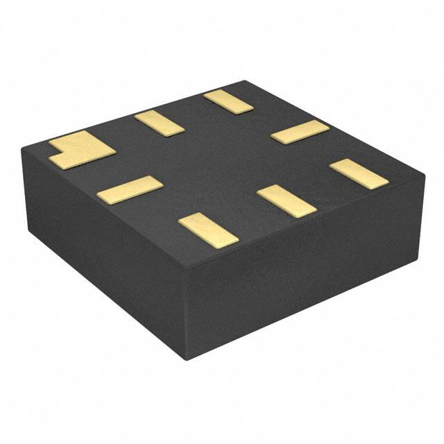
UQFN8
1.6X1.6, 0.5P
CASE 523AY
NC7WZ126
T6KK
XYZ
Description
The NC7WZ126 is a Dual Non−Inverting Buffer with independent
active HIGH enables for the 3−STATE outputs. The Ultra High Speed
device is fabricated with advanced CMOS technology to achieve
superior switching performance with high output drive while
maintaining low static power dissipation over a broad VCC operating
range. The device is specified to operate over the 1.65 V to 5.5 V VCC
operating range. The inputs and outputs are high impedance when
VCC is 0 V. Inputs tolerate voltages up to 5.5 V independent of VCC
operating range. Outputs tolerate voltages above VCC when in the
3−STATE condition.
Features
•
•
•
•
•
•
•
•
•
•
•
Space Saving US8 Surface Mount Package
MicroPak™ Pb−Free Leadless Package
Ultra High Speed: tPD 2.6 ns Typ. into 50 pF at 5 V VCC
High Output Drive: ±24 mA at 3 V VCC
Broad VCC Operating Range: 1.65 V to 5.5 V
Matches the Performance of LCX when Operated at 3.3 V VCC
Power Down High Impedance Inputs / Outputs
Overvoltage Tolerant Inputs Facilitate 5 V to 3 V Translation
Outputs are Overvoltage Tolerant in 3−STATE Mode
Patented Noise / EMI Reduction Circuitry Implemented
These Devices are Pb−Free, Halogen Free/BFR Free and are RoHS
Compliant
A1
OE1
EN
A2
OE2
EN
1
Y1
1
Y2
US8
CASE 846AN
T6, WZ26
KK
XY
Z
A
L
YW
WZ26
ALYW
= Specific Device Code
= 2−Digit Lot Run Traceability Code
= 2−Digit Date Code Format
= Assembly Plant Code
= Assembly Site
= Wafer Lot Number
= Assembly Start Week
ORDERING INFORMATION
See detailed ordering, marking and shipping information in the
package dimensions section on page 6 of this data sheet.
Figure 1. Logic Symbol
© Semiconductor Components Industries, LLC, 2005
June, 2022 − Rev. 3
1
Publication Order Number:
NC7WZ126/D
�NC7WZ126
Connection Diagrams
OE1
1
8
VCC
A1
2
7
OE2
OE1
7
A1
6
Y2
5
VCC 8
Y2
3
6
Y1
GND
4
5
A2
1
OE2
2
Y1
3
A2
Figure 3. Pad Assignments for MicroPak
(Top Thru View)
Figure 2. Connection Diagram
(Top View)
PIN DESCRIPTIONS
FUNCTION TABLE
Pin Names
OEn
4 GND
Description
Inputs
Enable Inputs for 3−STATE Outputs
Output
OE
An
Yn
An
Inputs
H
L
L
Yn
3−STATE Outputs
H
H
H
L
L
Z
L
H
Z
H = HIGH Logic Level
L = LOW Logic Level
Z = 3−STATE
www.onsemi.com
2
�NC7WZ126
ABSOLUTE MAXIMUM RATINGS
Symbol
Min
Max
Unit
VCC
Supply Voltage
−0.5
6.5
V
VIN
DC Input Voltage (Note 1)
−0.5
6.5
V
DC Output Voltage
−0.5
6.5
V
VOUT
Parameter
IIK
DC Input Diode Current
VIN < 0 V
−
−50
mA
IOK
DC Output Diode Current
VOUT < 0 V
−
−50
mA
IOUT
DC Output Source / Sink Current
−
±50
mA
DC VCC / GND Current
−
±100
mA
−65
+150
°C
ICC / IGND
TSTG
Storage Temperature Range
TJ
Junction Temperature under Bias
−
+150
°C
TL
Junction Lead Temperature (Soldering, 10 Seconds)
−
+260
°C
PD
Power Dissipation in Still Air
−
−
500
539
mW
US8
MicroPak−8
Stresses exceeding those listed in the Maximum Ratings table may damage the device. If any of these limits are exceeded, device functionality
should not be assumed, damage may occur and reliability may be affected.
1. The input and output negative voltage ratings may be exceeded is the input and output diode current ratings are observed.
RECOMMENDED OPERATING CONDITIONS
Symbol
VCC
VIN
VOUT
Parameter
Min
Max
Unit
Supply Voltage Operating
1.65
5.5
V
Supply Voltage Data Retention
1.5
5.5
0
5.5
V
Active State
0
VCC
V
3−State
0
5.5
V
Input Voltage
Output Voltage
TA
Operating Temperature
tr, tf
Input Rise and Fall Time
qJA
Thermal Resistance
−40
+85
°C
VCC = 1.8 V ±0.15 V, 2.5 V ±0.2 V
0
20
ns/V
VCC = 3.3 V ±0.3 V
0
10
VCC = 5.0 V ±0.5 V
0
5
−
−
250
232
US8
MicroPak−8
°C/W
Functional operation above the stresses listed in the Recommended Operating Ranges is not implied. Extended exposure to stresses beyond
the Recommended Operating Ranges limits may affect device reliability.
2. Unused inputs must be held HIGH or LOW. They may not float.
www.onsemi.com
3
�NC7WZ126
DC ELECTICAL CHARACTERISTICS
TA = +25°C
Parameter
Symbol
VIH
VIL
VOH
Conditions
TA = −40 to +85°C
Typ
Max
Min
Max
Unit
−
−
0.65 VCC
−
V
HIGH Level Input
Voltage
1.65 to 1.95 0.65 VCC
2.3 to 5.5
0.7 VCC
−
−
0.7 VCC
−
LOW Level Input
Voltage
1.65 to 1.95
−
−
0.35 VCC
−
0.35 VCC
2.3 to 5.5
−
−
0.3 VCC
−
0.3 VCC
1.65
1.55
1.65
−
1.55
−
2.3
2.2
2.3
−
2.2
−
3.0
2.9
3.0
−
2.9
−
4.5
4.4
4.5
−
4.4
−
IOH = −4 mA
1.65
1.29
1.52
−
1.29
−
IOH = −8 mA
2.3
1.9
2.15
−
1.9
−
IOH = −16 mA
3.0
2.4
2.80
−
2.4
−
IOH = −24 mA
3.0
2.3
2.68
−
2.3
−
IOH = −32 mA
4.5
3.8
4.20
−
3.8
−
IOL = 100 mA
1.65
−
0.0
0.10
−
0.10
2.3
−
0.0
0.10
−
0.10
3.0
−
0.0
0.10
−
0.10
4.5
−
0.0
0.10
−
0.10
IOL = 4 mA
1.65
−
0.08
0.24
−
0.24
IOL = 8 mA
2.3
−
0.10
0.3
−
0.3
IOL = 16 mA
3.0
−
0.15
0.4
−
0.4
IOL = 24 mA
3.0
−
0.22
0.55
−
0.55
IOL = 32 mA
4.5
−
0.22
0.55
−
0.55
HIGH Level Output
Voltage
VIN = VIH or
VIL
VIN = VIH or
VIL
VOL
VCC (V)
Min
LOW Level Output
Voltage
VIN = VIH or
VIL
VIN = VIH or
VIL
IOH = −100 mA
V
V
V
IIN
Input Leakage
Current
VIN = 5.5 V, GND
1.65 to 5.5
−
−
±0.1
−
±1
mA
IOZ
3−STATE Output
Leakage
VIN = VIH or VIL
0 ≤ VOUT ≤ 5.5 V
1.65 to 5.5
−
−
±0.5
−
±5
mA
IOFF
Power Off Leakage
Current
VIN or VOUT = 5.5 V
0.0
−
−
1
−
10
mA
ICC
Quiescent Supply
Current
VIN = 5.5 V, GND
1.65 to 5.5
−
−
1
−
10
mA
NOISE CHARACTERISTICS
TA = +25°C
VCC (V)
Typ
Max
Unit
VOLP (Note 3)
Quiet Output Maximum Dynamic VOL
CL = 50 pF
5.0
−
1.0
V
VOLV (Note 3)
Quiet Output Minimum Dynamic VOL
CL = 50 pF
5.0
−
1.0
V
VOHV (Note 3)
Quiet Output Minimum Dynamic VOH
CL = 50 pF
5.0
−
4.0
V
VIHD (Note 3)
Minimum HIGH Level Dynamic Input Voltage
CL = 50 pF
5.0
−
3.5
V
VILD (Note 3)
Maximum LOW Level Dynamic Input Voltage
CL = 50 pF
5.0
−
1.5
V
Symbol
Parameter
Conditions
3. Parameter guaranteed by design.
www.onsemi.com
4
�NC7WZ126
AC ELECTRICAL CHARACTERISTICS
TA = +25°C
Symbol
tPLH
tPHL
Parameter
Propagation Delay
An to Yn
(Figure 4, 6)
TA = −40 to +85°C
VCC (V)
Min
Typ
Max
Min
Max
Unit
1.8 ±0.15
−
−
12.0
−
13.0
ns
2.5 ±0.2
−
−
7.5
−
8.0
3.3 ±0.3
−
−
5.2
−
5.5
5.0 ±0.5
−
−
4.5
−
4.8
CL = 50 pF,
RD = 500 W
S1 = OPEN
3.3 ±0.3
−
−
5.7
−
6.0
5.0 ±0.5
−
−
5.0
−
5.3
Conditions
CL = 15 pF
RD = 1 MW
S1 = OPEN
tOSLH
tOSHL
Output to Output Skew
(Note 4) (Figure 4, 6)
CL = 50 pF,
RD = 500 W
S1 = OPEN
3.3 ±0.3
−
−
1.0
−
1.0
5.0 ±0.5
−
−
0.8
−
0.8
tPZL
tPZH
Output Enable Time
(Figure 4, 6)
CL = 50 pF
RD,RU = 500 W
S1 = GND for tPZH
S1 = VI for tPZL
VI = 2 x VCC
1.8 ±0.15
−
−
14.0
−
15.0
2.5 ±0.2
−
−
8.5
−
9.0
3.3 ±0.3
−
−
6.2
−
6.5
5.0 ±0.5
−
−
5.5
−
5.8
13.0
tPLZ
tPHZ
CIN
Output Disable Time
(Figure 4, 6)
CL = 50 pF
RD,RU = 500 W
S1 = GND for tPZH
S1 = VI for tPZL
VI = 2 x VCC
Input Capacitance
COUT
Output Capacitance
CPD
Power Dissipation
Capacitance (Figure 5)
(Note 5)
ns
ns
ns
1.8 ±0.15
−
−
12.0
−
2.5 ±0.2
−
−
8.0
−
8.5
3.3 ±0.3
−
−
5.7
−
6.0
5.0 ±0.5
−
−
4.7
−
5.0
0
−
2.5
−
−
−
pF
5.0
−
4
−
−
−
pF
3.3
−
10
−
−
−
pF
5.0
−
12
−
−
−
4. Parameter guaranteed by design. tOSLH = |tPLHmax − tPLHmin|; tOSHL = |tPHLmax − tPHLmin|.
5. CPD is defined as the value of the internal equivalent capacitance which is derived from dynamic operating current consumption (ICCD) at
no output loading and operating at 50% duty cycle. (see Figure 5) CPD is related to ICCD dynamic operating current by the expression:
ICCD = (CPD) (VCC) (fIN) + (ICCstatic).
www.onsemi.com
5
�NC7WZ126
AC Loading and Waveforms
VIN
OPEN
GND
VCC
OE INPUT
RU
OUTPUT
INPUT
CL
RD
CL includes load and stray capacitance
Input PRR = 1.0 MHz; tW = 500 ns
Figure 4. AC Test Circuit
VCC
A
INPUT
OE
OUTPUT
Input = AC Waveform; tr = tf = 1.8 ns;
PRR = 10 MHz; Duty Cycle = 50%.
Figure 5. ICCD Test Circuit
Figure 6. AC Waveforms
ORDERING INFORMATION
Top Mark
Package
Shipping†
NC7WZ126K8X
WZ26
8−Lead US8, JEDEC MO−187, Variation CA
3.1 mm Wide
3000 / Tape & Reel
NC7WZ126L8X
T6
8−Lead MicroPak, 1.6 mm Wide
(Pb−Free)
5000 / Tape & Reel
NC7WZ126L8X−L22185
T6
8−Lead MicroPak, 1.6 mm Wide
(Pb−Free)
5000 / Tape & Reel
Order Number
†For information on tape and reel specifications, including part orientation and tape sizes, please refer to our Tape and Reel Packaging
Specifications Brochure, BRD8011/D.
6. Pb−Free package per JEDEC J−STD−020B.
MicroPak is trademark of Semiconductor Components Industries, LLC (SCILLC) or its subsidiaries in the United States and/or other countries.
www.onsemi.com
6
�MECHANICAL CASE OUTLINE
PACKAGE DIMENSIONS
UQFN8 1.6X1.6, 0.5P
CASE 523AY
ISSUE O
0.05
C
A
1.60
DATE 31 AUG 2016
0.40
(6X)
1.60
B
0.45
(2X)
2X
1.60
TOP VIEW
PIN#1 IDENT
0.05
1.61
C
0.50
RECOMMENDED
LAND PATTERN
0.50±0.05
0.05
C
0.05
C
0.25
(8X)
NOTES:
SEATING
PLANE
0.025±0.025
A. PACKAGE CONFORMS TO JEDEC MO−255
VARIATION UAAD.
C
B. DIMENSIONS ARE IN MILLIMETERS.
SIDE VIEW
C. DIMENSIONS AND TOLERANCES PER
ASME Y14.5M, 2009.
1.60±0.05
(0.10)
D. LAND PATTERN RECOMMENDATION IS
EXISTING INDUSTRY LAND PATTERN.
(0.20)3X
DETAIL A
1
2
3
(0.20)
(0.09)
4
8
1.60±0.05
0.30±0.05
0.30±0.05 (7X)
7
6
5
0.50
1.00±0.05
(0.15)
0.20±0.05 (8X)
BOTTOM VIEW
DOCUMENT NUMBER:
DESCRIPTION:
98AON13591G
UQFN8 1.6X1.6, 0.5P
0.30±0.05
0.10
C
0.05
C
A
B
DETAIL A
SCALE : 2X
Electronic versions are uncontrolled except when accessed directly from the Document Repository.
Printed versions are uncontrolled except when stamped “CONTROLLED COPY” in red.
PAGE 1 OF 1
ON Semiconductor and
are trademarks of Semiconductor Components Industries, LLC dba ON Semiconductor or its subsidiaries in the United States and/or other countries.
ON Semiconductor reserves the right to make changes without further notice to any products herein. ON Semiconductor makes no warranty, representation or guarantee regarding
the suitability of its products for any particular purpose, nor does ON Semiconductor assume any liability arising out of the application or use of any product or circuit, and specifically
disclaims any and all liability, including without limitation special, consequential or incidental damages. ON Semiconductor does not convey any license under its patent rights nor the
rights of others.
© Semiconductor Components Industries, LLC, 2019
www.onsemi.com
�MECHANICAL CASE OUTLINE
PACKAGE DIMENSIONS
US8
CASE 846AN
ISSUE O
DOCUMENT NUMBER:
DESCRIPTION:
98AON13778G
US8
DATE 31 DEC 2016
Electronic versions are uncontrolled except when accessed directly from the Document Repository.
Printed versions are uncontrolled except when stamped “CONTROLLED COPY” in red.
PAGE 1 OF 1
ON Semiconductor and
are trademarks of Semiconductor Components Industries, LLC dba ON Semiconductor or its subsidiaries in the United States and/or other countries.
ON Semiconductor reserves the right to make changes without further notice to any products herein. ON Semiconductor makes no warranty, representation or guarantee regarding
the suitability of its products for any particular purpose, nor does ON Semiconductor assume any liability arising out of the application or use of any product or circuit, and specifically
disclaims any and all liability, including without limitation special, consequential or incidental damages. ON Semiconductor does not convey any license under its patent rights nor the
rights of others.
© Semiconductor Components Industries, LLC, 2019
www.onsemi.com
�onsemi,
, and other names, marks, and brands are registered and/or common law trademarks of Semiconductor Components Industries, LLC dba “onsemi” or its affiliates
and/or subsidiaries in the United States and/or other countries. onsemi owns the rights to a number of patents, trademarks, copyrights, trade secrets, and other intellectual property.
A listing of onsemi’s product/patent coverage may be accessed at www.onsemi.com/site/pdf/Patent−Marking.pdf. onsemi reserves the right to make changes at any time to any
products or information herein, without notice. The information herein is provided “as−is” and onsemi makes no warranty, representation or guarantee regarding the accuracy of the
information, product features, availability, functionality, or suitability of its products for any particular purpose, nor does onsemi assume any liability arising out of the application or use
of any product or circuit, and specifically disclaims any and all liability, including without limitation special, consequential or incidental damages. Buyer is responsible for its products
and applications using onsemi products, including compliance with all laws, regulations and safety requirements or standards, regardless of any support or applications information
provided by onsemi. “Typical” parameters which may be provided in onsemi data sheets and/or specifications can and do vary in different applications and actual performance may
vary over time. All operating parameters, including “Typicals” must be validated for each customer application by customer’s technical experts. onsemi does not convey any license
under any of its intellectual property rights nor the rights of others. onsemi products are not designed, intended, or authorized for use as a critical component in life support systems
or any FDA Class 3 medical devices or medical devices with a same or similar classification in a foreign jurisdiction or any devices intended for implantation in the human body. Should
Buyer purchase or use onsemi products for any such unintended or unauthorized application, Buyer shall indemnify and hold onsemi and its officers, employees, subsidiaries, affiliates,
and distributors harmless against all claims, costs, damages, and expenses, and reasonable attorney fees arising out of, directly or indirectly, any claim of personal injury or death
associated with such unintended or unauthorized use, even if such claim alleges that onsemi was negligent regarding the design or manufacture of the part. onsemi is an Equal
Opportunity/Affirmative Action Employer. This literature is subject to all applicable copyright laws and is not for resale in any manner.
PUBLICATION ORDERING INFORMATION
LITERATURE FULFILLMENT:
Email Requests to: orderlit@onsemi.com
onsemi Website: www.onsemi.com
◊
TECHNICAL SUPPORT
North American Technical Support:
Voice Mail: 1 800−282−9855 Toll Free USA/Canada
Phone: 011 421 33 790 2910
Europe, Middle East and Africa Technical Support:
Phone: 00421 33 790 2910
For additional information, please contact your local Sales Representative
�


 工商网监
湘ICP备2023018690号
工商网监
湘ICP备2023018690号
